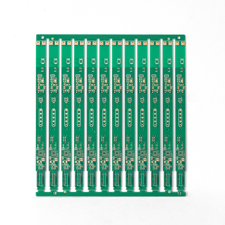
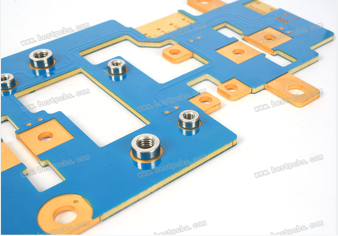
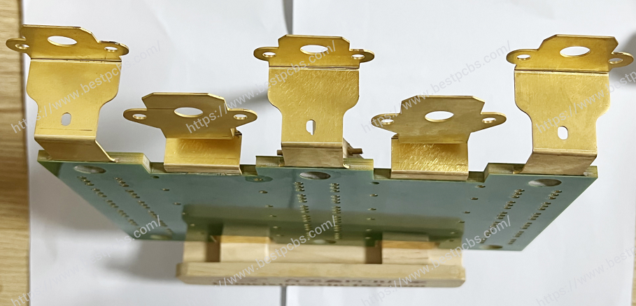
Flexible aluminum PCB is a new development in the recent years, it enables people decrease the size of certain products in some area. Different from the rigid flex PCB, flexible aluminum PCB combines the flex circuit and aluminum core circuit board (or can be copper core PCB), so it has the rigidity and good thermal management of traditional Aluminum PCBs with the flexibility of polyimide, these hybrid boards offer a host of advantages.
To increase the thermal conductivity in high power applications, and meet the flexibility requirements, flexible aluminum PCB is a good option. This article explores the key benefits of flexible Aluminum PCBs, highlighting why they are becoming increasingly popular in various applications.
What is Flexible Aluminum PCB?
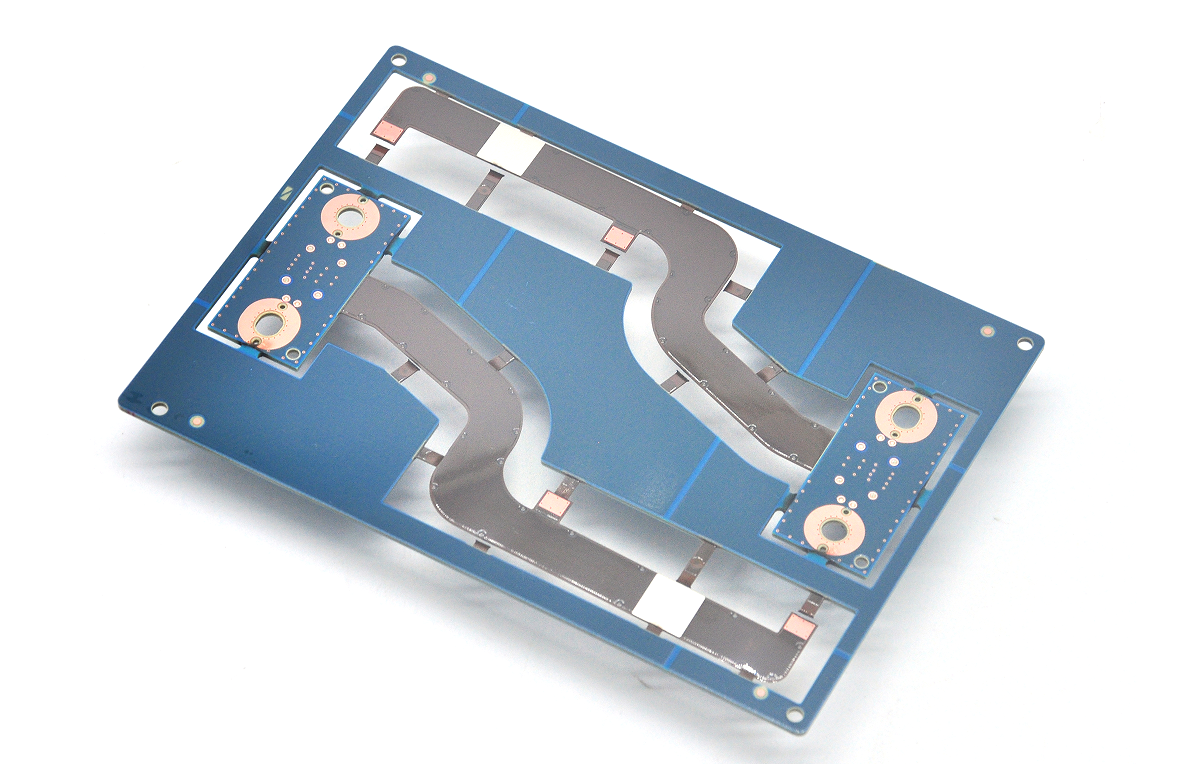
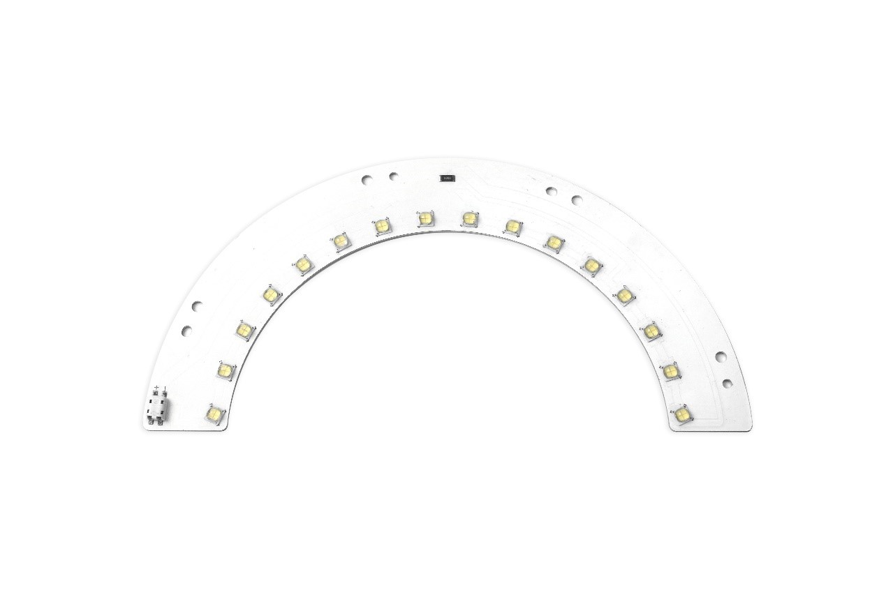
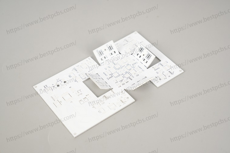
Flexible aluminum PCBs are a type of printed circuit board that uses an aluminum base material and is designed to be flexible. Unlike standard aluminum PCBs, these boards can bend and conform to different shapes, making them ideal for applications where space and flexibility are crucial. And Have you ever heard about our another aluminum board that we called bendable aluminum PCB? This is a special metal core circuit board that uses special material makes the circuit board bendable while won’t damage the board. May you think both of two are the same product? No, they are different in the constructure and raw materials, and the manufacturing processes are different as well.
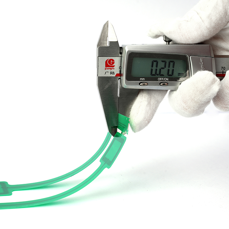
Bendable aluminum PCB uses aluminum alloy as the raw material, considering it must meet the bendable requirement as well as the good thermal management during using, it must be specially designed aluminum alloy composite material. And the aluminum base thickness also is a key consideration, 0.2mm to 1.0mm always are the common bending metal substrate thickness. Meanwhile, the bending radius of bendable aluminum PCB also should be calculated before manufacturing, making it follow the bending design standard to smooth the manufacturing. It is the same as flexible aluminum PCB.
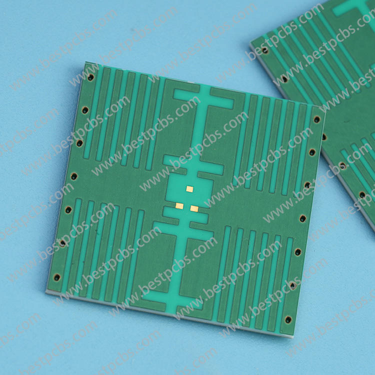
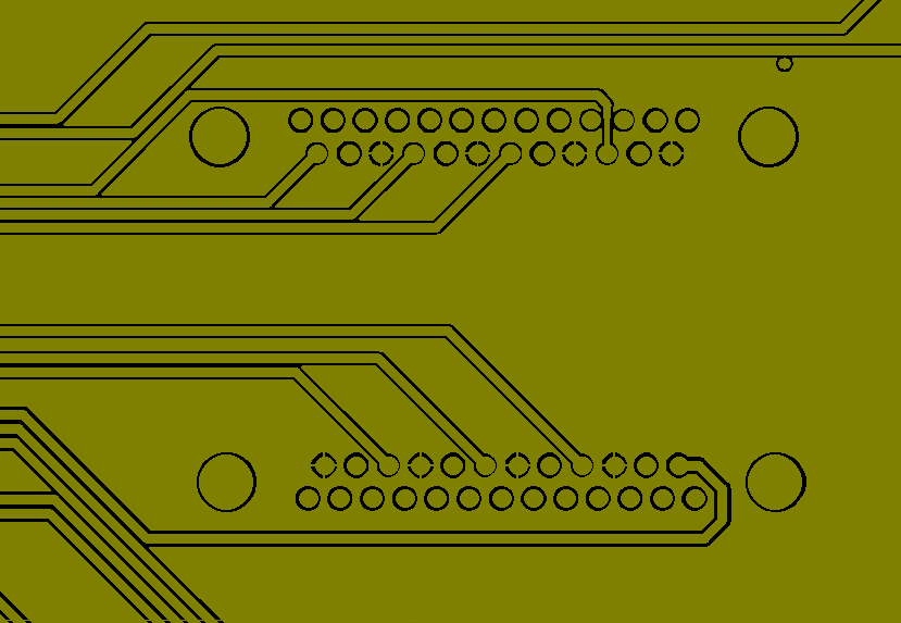
What Are the Constructure of Flexible Aluminum PCB?
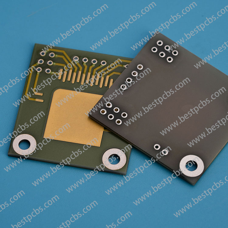
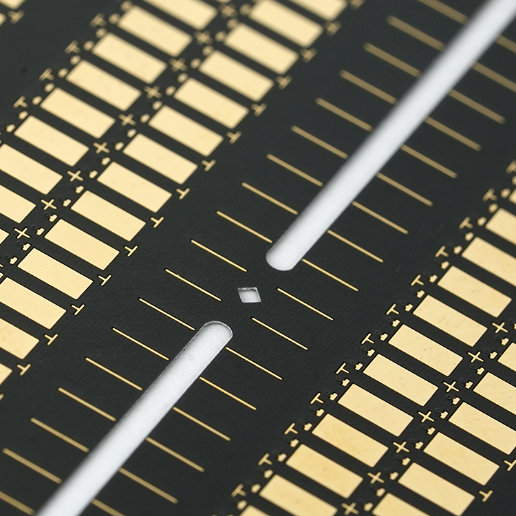
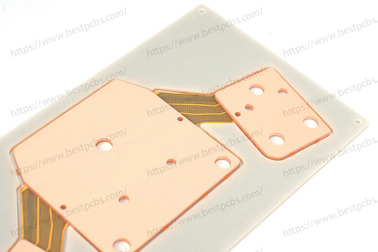
Flexible aluminum PCBs combine the benefits of aluminum’s excellent thermal management with the flexibility required for modern electronic designs. These PCBs are constructed using a combination of materials and layers that provide flexibility, durability, and efficient heat dissipation. And compared with original aluminum PCB, it adds the flexible insulation layer and the content of adhesive glue is different.
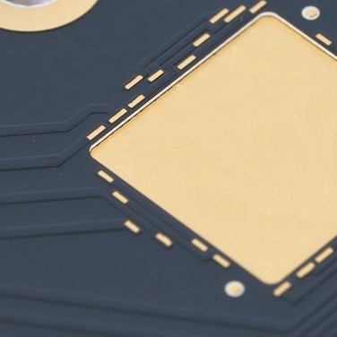
- Aluminum base layer
The aluminum base layer serves as the foundation of the flexible aluminum PCB. It provides structural support and excellent thermal conductivity. Typically, high-quality aluminum is used for this layer due to its superior thermal properties and mechanical strength.
- Dielectric layer
It acts an insulator between the aluminum base and copper foil, it can allow the heat pass through while electrically insulating the conductive pathways.
- Copper foil
The copper foil forms the conductive pathways that carry electrical signals and power across the PCB. It is essential for the functioning of the electronic components connected to the PCB.
- Flexible layer
Common materials for this layer include polyimide (PI) or polyester (PET), both known for their flexibility, thermal stability, and insulating properties. It contributes to the overall flexibility of the PCB, allowing it to bend and conform to various shapes.
- Protective overlayer
This layer is applied over the copper circuits to protect them from environmental factors such as moisture, dust, and physical damage. It also provides mechanical support to the flexible areas. Normally called solder mask layer.
The Difference Between Flexible Aluminum PCB and Flex Circuits
While both aluminum flex PCBs and flexible printed circuits (FPCs) offer flexibility, they differ significantly in their materials and manufacturing costs:
| Item | Flexible Aluminum PCB | Flex Circuit (FPC) |
| Base Material | Aluminum core | Polyimide or PET |
| Conductive Material | Copper foil and aluminum for the conductive traces | Various materials like polyimide, PET or the copper foil |
| Flexibility | Limited in specific area | Flexible everywhere |
| Thermal Conductivity | High thermal conductivity | Depends on the material used |
| Manufacturing Process | Complex | Relatively simple |
| Specific Advantage | Fast heat dissipation | General part in electronics |
| Cost | High | Cost-effective |
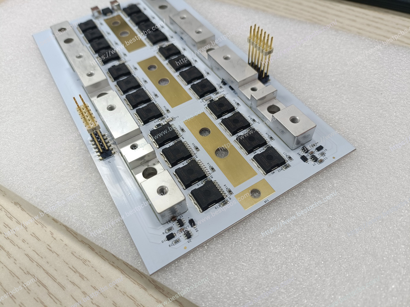
What Are the Benefits of Using Flexible Aluminum PCB?
Flexible aluminum PCB has numerous advantages that make it highly preferrable for specific applications, including:
- Excellent thermal management
Due to the applied of aluminum base, efficient heat dissipation prevents overheating and extends the lifespan of electronic components.
- Lightweight and flexible design
Due to the flexible and lightweight features in the flex aluminum PCB, it can be bent and shaped the PCB reduces the need for additional connectors and saves space in compact designs.
- Improve reliability
Aluminum based PCB has good durable, ensures the long-lasting performance of the whole product, even in harsh conditions.
- High density integrated
The flexible aluminum PCB allows for the higher density circuit layouts than normal aluminum PCB.
- Effective electromagnetic shielding
Aluminum material provides electromagnetic shielding in a certain degree, which helps to reduce the impact of electromagnetic interference on the circuit.
How to Choose A Reliable Flexible Aluminum PCB Manufacturer?
Selecting the right manufacturer for flexible aluminum PCBs is crucial for ensuring quality and reliability. Make sure your supplier has extensive experience in this field and obtained relevant certifications like UL, CE, ISO9001 and so on.
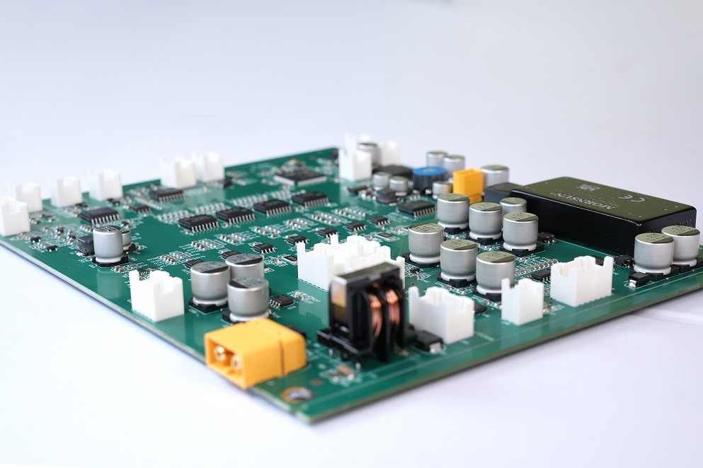
EBest Circuit (Best Technology) is a China-based PCB and PCBA manufacturer, who has over 17-years-experience circuit board manufacturing. At EBest Circuit (Best Technology), we specialize in providing high-quality flexible aluminum PCBs tailored to meet your specific needs. And we were certificated by ISO9001 quality control system, ISO13485 for medical device and IATF16949 for automotive system. Our expertise and commitment to excellence ensure that you receive the best solutions for your electronic applications. Choose EBest Circuit (Best Technology) for your PCB requirements and experience the benefits of advanced PCB technology.