PCB manufacturing PCB manufacturing
Home > Blog

IC Substrate

April 8th, 2026

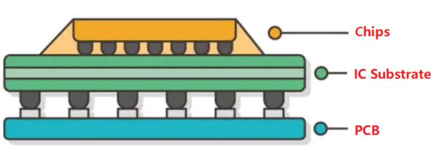
IC substrate is a core material in semiconductor packaging because it connects the chip to the circuit board, supports electrical transmission, and helps manage heat inside compact electronic products.

This article explains what an IC substrate is, how it is classified, which materials are commonly used, how it compares with PCB, and why it matters in modern electronics.
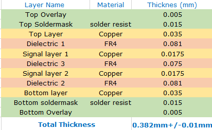
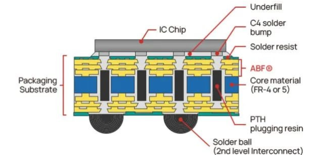
IC Substrate

IC Substrate

What Is an IC Substrate?

An IC substrate, also called an integrated circuit packaging substrate, is a critical material used in semiconductor packaging. It acts as the bridge between the silicon chip and the printed circuit board, carrying electrical signals, supporting the chip mechanically, and helping dissipate heat.

In modern electronic packaging, the IC substrate is far more than a simple base material. It plays a central role in improving signal transmission, enabling fine-pitch interconnection, reducing package size, and supporting advanced multi-chip integration. Because of this, IC substrates have become essential in high-performance and miniaturized electronic products.

As demand grows in sectors such as AI, 5G, cloud computing, servers, and big data, the IC substrate industry is expanding quickly. High-end chips need packaging platforms with tighter dimensional control, better thermal management, and higher routing density. That is exactly where IC substrates add value.

What Is an IC Substrate?

Why Is IC Substrate Important?

IC substrates are indispensable in the chip packaging and testing process because they provide several functions at once.

First, they support the chip physically and protect it during assembly and operation. Second, they create reliable electrical connections between the die and the main board. Third, they help manage heat, which is increasingly important in processors, GPUs, networking devices, and automotive electronics.

Compared with conventional interconnection methods, IC substrates can also improve package miniaturization. They make it possible to route more signals in a smaller area, support more input and output pins, and enhance overall electrical performance. In some advanced designs, they can even integrate passive or active components to support additional system functions.

How Are IC Substrates Classified?

IC substrates can be classified in several ways, including by packaging type, material characteristics, and bonding technology.

Classification by Packaging Type

BGA IC Substrate
Ball Grid Array substrates are widely used because they offer strong electrical and thermal performance. They are well suited for devices with high pin counts, especially packages with more than 300 pins.

CSP IC Substrate
Chip Scale Package substrates are used for compact single-chip packaging. They are lightweight and small, making them suitable for telecommunications devices, memory products, and other applications with relatively fewer pins.

FC IC Substrate
Flip-chip substrates are designed for high-speed and high-performance applications. They offer lower circuit loss, reduced signal interference, and better heat dissipation.

MCM IC Substrate
Multi-Chip Module substrates allow multiple chips with different functions to be integrated into a single package. They support compact and lightweight product designs, though thermal and signal management can become more challenging as package complexity rises.

Classification by Material

Rigid IC Substrate
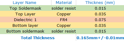
Rigid IC substrates are commonly made from ABF resin, BT resin, or epoxy resin. They usually have a coefficient of thermal expansion around 13–17 ppm/°C and are widely used in mainstream packaging.

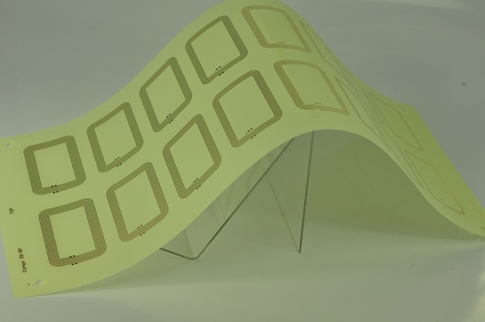
Flexible IC Substrate
Flexible IC substrates are usually made from PI or PE resin. Their flexibility makes them useful in space-constrained designs and applications requiring bending or lightweight packaging.

Ceramic IC Substrate
Ceramic IC substrates use materials such as alumina, aluminum nitride, or silicon carbide. These substrates have lower thermal expansion and better thermal performance, making them suitable for demanding environments.

Classification by Bonding Technology

The main bonding methods used in IC substrate packaging include:

  • Tape-Automated Bonding (TAB)
  • Wire Bonding
  • Flip-Chip Bonding

Each method has its own packaging advantages depending on electrical performance, package size, cost, and design requirements.

What Materials Are Used in IC Substrates?

The main raw materials used in IC substrates today include BT substrates, ABF substrates, and glass substrates.

BT Substrate

BT substrate uses bismaleimide triazine resin as the base material. It offers high glass transition temperature, good heat resistance, and a relatively low dielectric constant. These properties make it suitable for products that require stable electrical performance and good reliability.

BT substrates are commonly used in memory chips, MEMS devices, RF chips, and LED packaging. As demand for servers and memory continues to grow, BT substrates remain an important material in the packaging supply chain.

ABF Substrate

ABF stands for Ajinomoto Build-Up Film. ABF substrates are known for enabling fine line widths, small spacing, and high-density interconnection. These features make them highly suitable for advanced packaging with high pin counts and high data rates.

They are widely used in CPU, GPU, FPGA, and ASIC packaging, especially in high-performance computing. With rapid growth in AI, cloud computing, and 5G infrastructure, ABF substrates have become one of the most valuable materials in advanced semiconductor packaging.

At the same time, ABF materials must keep evolving. As package sizes increase and performance targets become stricter, substrate materials need better dimensional stability, stronger thermal reliability, and improved process compatibility.

Glass Substrate

Glass substrate is an emerging material in semiconductor packaging. It provides excellent mechanical stability and attractive physical properties. Compared with traditional materials, glass can reduce pattern distortion, improve photolithography accuracy, and support much higher via density.

Glass substrates are also seen as promising for ultra-large package formats. According to industry analysis, they may offer advantages in performance, density, power efficiency, and long-term cost structure. Although still developing, they are becoming an important topic in next-generation packaging.

What Materials Are Used in IC Substrates?

IC Substrate vs. PCB: What Is the Difference?

Although IC substrates and PCBs are closely related, they are not the same.

1. Basic Definition

An IC substrate is mainly used in chip packaging. It connects the semiconductor die to the printed circuit board and supports fine-pitch, high-density electrical routing.

A PCB, by contrast, is the board used to mount and connect electronic components in a finished product. It serves as the platform for system-level assembly in devices such as computers, telecom equipment, industrial controls, and medical electronics.

2. Design Features

IC substrate design focuses heavily on miniaturization, precision, and electrical performance. It must support fine traces, tight spacing, and advanced signal routing within a very limited area. Thermal control and noise reduction are also major design concerns.

PCB design is broader in system scope. It must consider materials, stackup, EMI performance, manufacturability, and cost. While precision is still important, the design rules are generally less extreme than those of IC substrates.

3. Manufacturing Process

IC substrate manufacturing uses highly advanced processes such as deposition, exposure, fine etching, molding, and laser processing. The precision requirements are much closer to semiconductor fabrication than to standard board production.

PCB manufacturing includes drilling, plating, imaging, etching, solder mask application, surface finishing, testing, and assembly preparation. While both IC substrates and PCBs rely on circuit patterning and interconnection technologies, IC substrate production is generally more demanding in terms of dimensional tolerance and feature size.

Even though they differ in function and process complexity, IC substrates and PCBs work together in electronic products. The IC substrate connects the chip to the package level, while the PCB connects the package to the complete system.

What Are the Main Applications of IC Substrates?

IC substrates are used in a wide range of industries because they support high-density packaging, compact product design, and reliable electrical performance.

Common applications include:

  • Consumer electronics such as smartphones, tablets, laptops, and wearables
  • Automotive electronics including ADAS, infotainment systems, and EV power/control modules
  • Telecommunications such as 5G infrastructure and networking hardware
  • Medical devices including implantable electronics and diagnostic systems
  • Aerospace and defense applications such as radar, satellites, and surveillance systems
  • Industrial equipment including robotics and factory automation
  • AI and sensor modules requiring advanced data processing and compact packaging

As chip performance rises, these application areas increasingly rely on advanced substrate technology to meet electrical, thermal, and size requirements.

What Is IC Substrate Packaging?

IC substrate packaging refers to the stage in semiconductor production where the chip is enclosed in a protective package and electrically connected for use in electronic systems. The package protects the die from environmental damage while enabling electrical communication with the PCB.

Several packaging formats are commonly used:

  • PGA (Pin Grid Array) for socket-based connections
  • DIP (Dual Inline Package) for through-hole assembly
  • CSP (Chip Scale Package) for highly compact surface-mount designs
  • QFP (Quad Flat Package) for leaded surface-mount packages
  • QFN (Quad Flat No-Lead) for compact, leadless surface mounting
  • MCP (Multi-Chip Package) for integrating multiple dies in one package
  • Area Array Package for efficient high-density interconnection across the full package surface

The choice of package depends on product size, thermal requirements, electrical performance, assembly method, and cost targets.

What Is IC Substrate Packaging?

What Is IC Substrate Packaging?

What Are the Key Features of IC Substrates?

IC substrates stand out because they are engineered for demanding electrical and mechanical performance. Their key features include:

High Interconnection Density

They support a large number of chip-to-board connections in a compact space, often through multilayer structures.

Strong Signal Integrity

Low-loss materials and precision routing help preserve high-speed and high-frequency signal quality.

Thermal Management

Substrate materials and structures are designed to help conduct and spread heat, which is critical in processors, power devices, and automotive systems.

Mechanical Reliability

IC substrates must withstand thermal cycling, vibration, and mechanical stress while maintaining stable interconnection.

Miniaturization Support

They enable narrow traces, small vias, fine pitch, and dense component integration, which are all needed in compact electronics.

Multi-Layer Capability

Multiple conductive layers allow more complex routing and better integration of electrical functions.

Moisture and Corrosion Resistance

Many substrate materials and protective finishes help improve long-term reliability in harsh operating environments.

How Is the IC Substrate Market Evolving?

The IC substrate market is moving toward higher density, thinner structures, better thermal stability, and stronger support for advanced computing. AI servers, high-speed networking, automotive electronics, and 5G devices are all pushing packaging requirements higher.

ABF substrates are seeing strong demand because they are widely used in high-performance computing chips. BT substrates continue to serve important roles in memory and RF packaging. Glass substrates are also attracting industry attention as a possible next-generation platform for very large and very advanced packages.

In the coming years, manufacturers that can offer precise process control, better yield, and material innovation will be in a strong position within the IC substrate supply chain.

FAQ About IC Substrate

1. What is the function of an IC substrate?

Its main function is to support the chip, connect it electrically to the board, help dissipate heat, and improve package miniaturization and performance.

2. Is IC substrate the same as PCB?

No. An IC substrate is mainly used in semiconductor packaging, while a PCB is used in finished electronic assemblies. The IC substrate connects the chip to the package level, and the PCB connects the package to the wider system.

3. What materials are commonly used in IC substrates?

BT substrate, ABF substrate, and glass substrate are the main material groups highlighted in your source content. Ceramic materials are also used in specific high-reliability or thermal-demanding designs.

4. Why is ABF substrate important?

Because it supports finer circuitry, high pin counts, and high-speed transmission, making it highly suitable for CPU, GPU, FPGA, ASIC, and HPC packaging.

5. What is the difference between ABF and BT substrate?

BT substrate is widely used in memory, MEMS, RF, and LED chip packaging, while ABF substrate is more closely tied to advanced, high-pin-count, high-speed packaging.

6. Is glass substrate already used in advanced packaging?

It is emerging as a serious next-generation material. Your source describes it as offering better mechanical stability, lower distortion, and much higher via density potential.

Extra Thin PCB

April 8th, 2026

Extra thin PCB refers to a printed circuit board with a significantly reduced thickness compared to standard FR4 boards, enabling compact, lightweight, and space-constrained electronic designs.

As modern devices become smaller and more integrated, ultra thin PCB solutions are increasingly used in smart cards, wearable devices, and miniature modules where every micron matters.

Are You Facing These Challenges?

Many customers come to us with similar design concerns:

  • The product housing leaves very little board space
  • Standard PCB thickness is too bulky for the assembly
  • Flexible PCB is not necessary, but standard rigid PCB is too thick
  • Thin boards may warp or become hard to handle in production
  • Small electronic modules need a lighter and slimmer rigid solution

Our extra thin PCB service is built to solve these issues with practical FR4-based manufacturing support.

What Is an Extra Thin PCB?

An extra thin PCB is a rigid printed circuit board with a thickness significantly lower than a normal FR4 board. Standard PCB thickness is usually around 1.0 mm to 2.0 mm. In thinner conventional constructions, 1-layer or 2-layer boards may be made at 0.3 mm to 0.4 mm, while 4-layer boards are often around 0.6 mm.

When electronic products require an even slimmer profile, designers may specify thicknesses such as 0.25 mm, 0.20 mm, or 0.15 mm. These ultra-slim boards are commonly referred to as extra thin PCB, ultra thin PCB, or very thin PCB.

They are especially useful in products where every fraction of a millimeter affects housing design, connector fit, weight, or assembly clearance.

Click here to see more pictures of our ultra thin PCB boards.

Extra Thin PCB

Extra Thin PCB

Why Use Extra Thin PCB?

As consumer and industrial devices continue moving toward lighter and more compact designs, extra thin PCBs are becoming more widely used. They help optimize the internal layout without forcing a full shift to flexible circuits.

Key benefits include:

  • Reduced product thickness
  • Lower overall weight
  • Better fit for compact assemblies
  • More rigid than flexible circuits
  • More cost-effective than FPC in many simple designs
  • Suitable for slim modules with limited installation space

In some applications, extra thin FR4 PCB can also provide slight bendability during assembly. It does not replace a true flex circuit, but it can offer more mechanical tolerance than a standard rigid board.

Extra Thin PCB Applications

Extra thin PCBs are commonly used in products that demand a slim form factor and stable board structure. Typical applications include:

  • SIM card modules
  • TF card modules
  • NFC devices
  • Mobile phone charging modules
  • Wearable electronics
  • Drawing tablets
  • Metro coins or smart token devices

These products often have very limited internal clearance, making thin board construction an important part of the mechanical design.

Extra Thin PCB Manufacturing Capability

EBest Circuit provides extra thin PCB fabrication with the following capability range:

ItemCapability
Base MaterialFR4 Tg130, Tg170, Tg180
Board Thickness0.10 mm to 0.30 mm
Copper Thickness0.5 oz, 1 oz, 2 oz, 3 oz
Outline ProcessingRouting, punching, V-cut, laser cutting
Solder MaskBare, white, black, blue, green, red
Silkscreen ColorBlack, white
Surface FinishImmersion gold, OSP, ENEPIG, HAL-LF
Max Panel Size500 × 500 mm or 1000 × 350 mm
Min Panel Size3.5 × 3.5 mm
Min Single Size25 × 25 mm
Min Via Size0.10 mm
Min Trace / Space4/4 mil
PackingVacuum packing
Sample Lead Time7 to 9 days
Mass Production Lead Time8 to 10 days

We can manufacture extra thin boards with or without solder mask, depending on the design and end-use requirement.

Extra Thin PCB vs Flexible PCB

Although they may look similar in ultra-slim products, extra thin PCB and flexible PCB serve different purposes.

Extra Thin PCB

  • FR4-based rigid board
  • Better structural support
  • Easier for handling and assembly
  • Usually lower cost than FPC in comparable simple layouts
  • Suitable when slight thinness is needed, but repeated bending is not required

Flexible PCB

  • Built on polyimide or other flexible materials
  • Designed for dynamic bending or folding
  • Better choice for extremely thin or moving interconnect structures
  • Suitable when board thickness must go below 0.10 mm or when repeated flexing is required

If your design needs a board below 0.10 mm, a flex circuit is generally the better option. If you need a thin, stable, and economical rigid board, extra thin FR4 PCB is often the more practical solution.

Stack-Up of Extra Thin PCB

The construction of extra thin PCB is similar to standard FR4 PCB, but the material system is thinner and the process window is tighter. The board uses thinner core materials and prepregs to achieve the required final thickness.

Because the structure is much thinner, stack-up design becomes more sensitive. Material choice, copper balance, and lamination control all affect flatness, handling strength, and final dimensional stability.

For 2-layer to 4-layer extra thin PCBs, the stack-up is usually simpler than conventional multilayer boards, but it must still be engineered carefully to maintain production consistency.

2L PCB structure for extra thin PCB

Stack-Up of Extra Thin PCB

4L PCB structure for extra thin PCB

Stack-Up of Extra Thin PCB

How Are Extra Thin PCBs Manufactured?

The basic fabrication flow is close to standard FR4 PCB manufacturing, but extra thin boards require tighter control at every stage. Thin materials are easier to deform during drilling, imaging, etching, lamination, routing, and transportation through the production line.

To support reliable production, EBest Circuit uses stricter handling methods and more precise process control for extra thin boards. In some operations, dedicated equipment or supporting fixtures are used to improve stability and reduce the risk of deformation or damage.

This is especially important for:

  • Panel handling
  • Warpage control
  • Fine drilling accuracy
  • Outline precision
  • Surface protection
  • Final packing and shipment stability

Careful process control helps ensure that the finished boards meet both dimensional and reliability requirements.

Why Choose EBest Circuit for Extra Thin PCB?

Choosing the right supplier for extra thin PCB is not only about whether thin boards can be produced. It is also about whether the manufacturer can keep those boards stable, consistent, and practical for real assembly conditions.

At EBest Circuit, we provide:

  • Extra thin FR4 PCB fabrication for compact designs
  • Thickness options from 0.10 mm to 0.30 mm
  • Multiple copper weights and surface finishes
  • Prototype and volume production support
  • Engineering review before production
  • Stable manufacturing control for delicate thin boards
  • Fast lead times for samples and mass production

We understand the common manufacturing risks behind ultra-thin rigid boards and work to reduce handling issues before they become assembly problems.

Work with a Reliable Extra Thin PCB Manufacturer | EBest Circuit

If your project requires a thinner rigid board for compact electronics, EBest Circuit can help you move from design to production with stable manufacturing support.

We offer extra thin PCB solutions for card devices, wearable products, NFC modules, charging applications, and other slim electronic assemblies. Whether you need a prototype or volume production, our team can support your design with suitable materials, practical fabrication control, and responsive engineering service.

Looking for a dependable extra thin PCB manufacturer? Contact EBest Circuit today to discuss your project and request a quote.

FAQs About Extra Thin PCB

1. What is the thinnest PCB you can manufacture?

We can produce extra thin PCBs down to 0.10 mm using FR4 materials. For thinner requirements, flexible PCB is recommended.

2. Can extra thin PCB replace flexible PCB?

No. Extra thin PCB offers slight bendability but is not designed for dynamic flexing. For bending applications, FPC is required.

3. Is ultra thin PCB more expensive?

It is slightly higher than standard PCB due to tighter process control, but still more cost-effective than flexible PCB.

4. What copper thickness is supported?

We support 0.5 oz, 1 oz, 2 oz, and 3 oz depending on current and design requirements.

5. How do you prevent warpage in thin PCB?

We use optimized lamination parameters, panel support fixtures, and controlled handling processes to ensure flatness.

6. What industries use extra thin PCB the most?

Smart cards, wearable devices, consumer electronics, and compact modules are the most common applications.

Need Ultra Thin PCB for Your Project?

If your design requires a compact, lightweight, and reliable PCB solution, extra thin PCB is a practical choice.

Contact EBest Circuit today for a fast quote and free DFM review.

Email: sales@bestpcbs.com
Phone: +86-755-2909-1601

We help you turn complex thin PCB designs into stable, production-ready solutions.

Bus Bar PCB

April 8th, 2026

EBest Circuit (Best Technology) brings nearly 20 years of PCB manufacturing experience to high-current and power distribution projects. We provide one-stop support for bus bar PCB solutions, covering layout review, engineering evaluation, prototyping, mass production, and after-sales service.

Our manufacturing system is backed by ISO9001, ISO13485, IATF16949, and UL certifications, helping customers build reliable products for demanding industries. Whether you need a custom embedded bus bar PCB, copper inlay PCB, or extruded copper PCB, our team can tailor the structure to your current, thermal, and mechanical requirements.

What is Bus Bar PCB?

bus bar PCB, also known as an embedded bus bar, busbar PCB, extruded copper PCB, or copper inlay PCB, is a specialized type of heavy copper PCB designed specifically to distribute power efficiently across different components on a board. Unlike traditional PCBs, which use copper traces etched into layers of non-conductive substrate to form circuits, bus bar PCBs integrate thick, solid bars of conductive material—often copper or aluminum—to handle higher currents.

The bus bar PCBs can also serve as mechanical connectors within the system, designed to accommodate screws and other metal parts for direct connections with other PCBs or system components.

Bus Bar PCB

Advantages of Bus Bar PCB

  • The PCB stiffener busbars can increase the rigidity and strength of circuit boards, so they can be used in severe environments like automotives, military instruments, aerospace, etc.
  • Higher power distribution and current-carry capabilities for power supply circuits or high-power applications.
  • The low voltage drop characteristic allows all components to maintain stable power delivery, especially under high load conditions.
  • The conductive bars in bus bar PCBs acts as an effective heat sink, helping to dissipate heat more efficiently than standard fiberglass PCBs, avoiding overheating problems during use.
  • The ability to handle higher currents simplifies the design and assembly process without the need for multiple layout or complex traces.
  • Bus bar PCBs can be used as electrical conduit, can also be used as mechanical connector.
  • They are often custom designed to meet specific application requirements, providing solutions that are not possible with standard PCB technology.

Basic Parameter of Bus Bar PCB Manufacturing

At EBest Circuit, bus bar PCB manufacturing can be customized according to current demand, installation method, and product structure. Typical capabilities include:

  • Minimum spacing between copper bars: 0.8–1.0mm
  • Copper bar thickness: 1.0–3.0mm
  • Current carrying capacity: 50–300A
  • Copper bar forming: bars can be bent based on project requirements
  • Surface finish options: ENIG, immersion silver, gold plating
  • Board thickness: 3.0–6.0mm
  • Hole wall copper thickness: ≥25um
  • Aspect ratio: 1:6 or 1:7
  • Example: for 1.0mm copper, minimum hole size can be 0.7mm
  • Layer count: typically 3–4 layers, with additional layers available after engineering review
  • Maximum dimension is 600*400mm for standard bus bar PCB, 900*600mm for double sided PCB
  • The lead time of 3-4L bus bar PCB is around 13-15days, add 3days per layer over 4 layers.

These values may vary depending on the bus bar design, material selection, drilling limitations, and final assembly requirements.

Design Guide for Bus Bar PCB

  • Copper or aluminum is typically used for the bus bars due to their excellent conductivity and thermal properties. Copper is more conductive, while aluminum is lighter and offers better resistance to oxidation.
  • Choose substrates capable of handling high thermal loads and providing good electrical insulation. Common material we used is FR-4.
  • Determine the maximum current that each busbar needs to carry, so we can know the required cross-sectional area of the bus to minimize drag and heat buildup.
  • Use the length of the bus and the resistivity of the material to calculate the allowable voltage drop on the bus to ensure that it remains within an acceptable range.
  • Add mechanical mounting points to the bus, such as screw holes or connector slots.
  • Consider the mechanical stresses that the PCB may encounter, ensuring that the bus is flexible enough to withstand bending and strong enough to support structural loads.

Where Are Bus Bar PCBs Used?

Bus bar PCBs are used in products that require strong current handling, efficient heat control, and compact power routing. Common applications include:

  • Electric vehicles
  • Renewable energy systems
  • Industrial automation equipment
  • Power distribution units
  • Data center power systems
  • High-power spacecraft electronics
  • Consumer electronics with heavy current demand
  • Power inverters and converters
  • Aerospace and defense systems

In these fields, designers often need a solution that goes beyond standard heavy copper routing. Bus bar PCBs provide a practical way to combine power transmission, thermal performance, and mechanical integration in one board structure.

Need a Custom Bus Bar PCB?

If you are developing a high-current product and need a reliable bus bar PCB manufacturer, EBest Circuit can help. We support custom structures based on your current load, board dimensions, copper thickness, thermal requirements, and assembly needs.

Send us your drawings, Gerber files, or project requirements, and our team will review the design and provide a suitable manufacturing solution.