

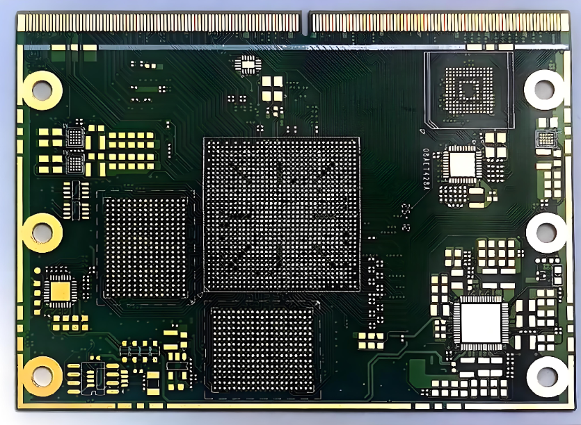
HDI PCB, or High Density Interconnect printed circuit board, is built for electronic products that demand more routing space, finer features, smaller vias, and higher circuit density in a limited footprint. Compared with conventional PCB structures, HDI boards support finer lines and spaces, smaller capture pads, and more interconnections per unit area, making them ideal for compact, lightweight, and high-speed devices.
At Best Technology, we provide standard HDI PCB, HDI flex PCB, 2–16 layer HDI multilayer PCB, any-layer HDI PCB, rigid-flex PCB, and high-frequency PCB solutions for customers who need reliable performance, stable manufacturing, and fast turnaround. Our uploaded source also states a monthly production capacity of 260,000 square feet (28,900 square meters), with expedited service available for urgent projects.
What Is HDI PCB?
HDI PCB is the abbreviation of High Density Interconnect PCB. It is a printed circuit board designed with high integration, high precision, and miniaturized interconnection structures. HDI technology uses advanced processes such as microvia formation, via filling, and metallized interconnection to achieve reliable signal transmission and dense circuit routing.
In practical terms, HDI PCB helps designers place more functions into a smaller board area. This makes it a preferred solution for modern electronics that require smaller product size, lighter weight, faster data transfer, and improved electrical performance. The source material describes HDI boards as having finer lines and spaces below 100 μm, smaller vias below 150 μm, and smaller capture pads below 400 μm than conventional PCB technology.
Why Choose HDI PCB?
HDI PCB is widely used because it gives engineers more design freedom without sacrificing reliability.
Higher Circuit Density
HDI boards use tighter routing, smaller line width and spacing, and more advanced via structures. This allows more components and more functions to fit into the same board outline.
Better Signal Performance
Shorter signal paths and lower impedance help reduce signal delay and transmission loss. This is especially valuable in high-speed digital and high-frequency electronic applications.
Smaller and Lighter Product Design
HDI construction supports thinner, lighter, and more compact products. It is well suited to the ongoing trend toward portable and space-saving electronics.
Strong Reliability
With precise layer buildup, microvia structures, and better interlayer support, HDI boards can provide stable electrical performance and dependable mechanical structure in demanding assemblies.
Our HDI PCB Capabilities
We support a wide range of HDI PCB manufacturing solutions for both prototype and production requirements, including:
| Item | Capability |
| Layer Count | 2–16 Layers (HDI), Any-Layer HDI Available |
| Min Line Width / Space | 3/3 mil (HDI) |
| Min Via Size | ~4 mil (Laser Microvia) |
| Via Type | Blind, Buried, Microvia, Via-in-Pad |
| Copper Thickness | 0.5 oz – 3 oz |
| Surface Finish | ENIG, ENEPIG, OSP, HASL, Immersion Silver |
| Board Thickness | 0.2 mm – 3.2 mm |
| BGA Capability | Down to 0.3–0.4 mm pitch |
| Material Options | FR4, High-Tg, Low Dk/Df, Polyimide |
| Max Panel Size | Up to 1200 mm × 360 mm |
| Testing | AOI, X-Ray, Flying Probe, ICT |
We also support fast-response manufacturing for urgent orders. According to the provided content, urgent boards can be shipped within 24 hours under suitable project conditions.
HDI PCB Types
According to layer up different, currently DHI board is divided into three basic types:
1) HDI PCB (1+N+1)
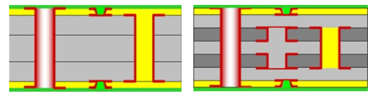
Features:
- Suitable for BGA with lower I/O counts
- Fine line, microvia and registration technologies capable of 0.4 mm ball pitch
- Qualified material and surface treatment for Lead-free process
- Excellent mounting stability and reliability
- Copper filled via
Application: Cell phone, UMPC, MP3 Player, PMP, GPS, Memory Card
2) HDI PCB (2+N+2)
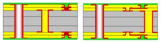
Features:
- Suitable for BGA with smaller ball pitch and higher I/O counts
- Increase routing density in complicated design
- Thin board capabilities
- Lower Dk / Df material enables better signal transmission performance
- Copper filled via
Application: Cell phone, PDA, UMPC, Portable game console, DSC, Camcorder
3) ELIC (Every Layer Interconnection)
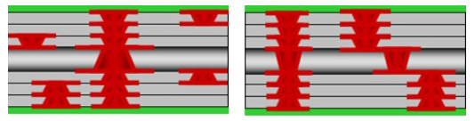
Features:
- Every layer via structure maximizes design freedom
- Copper filled via provides better reliability
- Superior electrical characteristics
- Cu bump and metal paste technologies for very thin board
Application: Cell phone, UMPC, MP3, PMP, GPS, Memory card.
What is HDI Material?
1. Substrate
The substrate is the basis of HDI PCB. Commonly used organic insulating materials include thermosetting resins (such as phenolic resins and epoxy resins) and thermoplastic polyesters (such as polyimide and polytetrafluoroethylene). The choice of substrate depends on the needs of specific applications, such as rigid or flexible PCBs.
2. Copper foil
As a conductive material, the thickness of copper foil is generally between 0.3mil-3mil. The specific choice depends on the current carrying size and etching accuracy. The quality of copper foil directly affects the surface quality and electrical performance of the product.
3. PP (B-stage resin)
When making multi-layer PCBs, PP is an indispensable material as an interlayer adhesive.
4. Photosensitive materials
Including photoresists and photosensitive films, divided into wet films and dry films. These materials will undergo chemical changes under light of a specific wavelength, affecting their solubility in the developer, thereby achieving precise production of circuits.
5. Solder mask (ink)
As a solder mask, solder mask is used to prevent the adhesion of liquid solder, and its performance affects the welding quality and circuit protection of PCBs.
6. Film
Similar to the polyester film used for photography, the film is used to record image data and requires high contrast, sensitivity and resolution while ensuring fine lines and dimensional stability.
HDI PCB Manufacturing Process
The uploaded source outlines a typical HDI PCB manufacturing flow, covering the core steps from design to final inspection.
1. Design Review – define the circuit structure, layer count, and stackup
2. Material Preparation – prepare substrate, copper-clad material, covering layers, and inner layers
3. Laser Drilling – create small vias for interlayer electrical connection
4. Lamination – press the inner and outer layers into a stable structure
5. Etching – remove excess copper and keep the required conductive pattern
6. Plating – improve conductivity and oxidation resistance
7. Assembly – insert and solder components if assembly service is included
8. Testing and Inspection – verify quality and electrical performance
Typical Applications
HDI PCB is widely used in products that require compact design and high functional density. The original material lists applications such as:
- Cell Phones
- UMPC
- PDA
- GPS Devices
- Memory Cards
- Portable Game Consoles
- Digital Cameras
- Camcorders
- Notebook Computers
- Network Communication Equipment
- Chip Carriers for Large-Scale IC Packaging
Why Work With EBest Circuit?
We position HDI PCB service around what engineering teams and sourcing teams actually need: broad process coverage, quick response, stable quality, and one-stop manufacturing support. The source content also highlights experience in high-end HDI, multilayer PCB, high-frequency PCB, high-speed PCB, FPC, rigid-flex PCB, SMT processing, and PCBA OEM service.
What You Can Expect
- Wide HDI product range
- Prototype to production support
- Fast turnaround for urgent projects
- One-stop PCB and PCBA service
- Competitive pricing with manufacturing support
FAQs About HDI PCB
1. What is the difference between HDI PCB and standard PCB?
HDI PCB uses finer lines, smaller vias, and higher connection density, allowing more circuits in less space compared to standard PCB.
2. When should I use HDI PCB?
HDI is recommended when your design includes fine-pitch BGA, high-speed signals, or strict space constraints.
3. Is HDI PCB more expensive?
Yes, due to more complex processes and tighter tolerances. However, it can reduce overall system size and improve performance.
4. What is the minimum via size in HDI PCB?
Typically around 4 mil (laser drilled microvia), depending on manufacturer capability.
5. Can HDI PCB improve signal integrity?
Yes. Shorter routing paths and better layer control can improve signal performance in high-speed designs.
6. How long does HDI PCB manufacturing take?
Prototype lead time can be as fast as 24 hours, while standard production depends on complexity and volume.
Get a Quote for Your HDI PCB Project
If your project requires microvias, fine-pitch BGA routing, higher wiring density, or compact multilayer construction, HDI PCB may be the right solution. A well-designed HDI board can help reduce product size, improve routing efficiency, and support stronger electrical performance in advanced electronics.
Send us your Gerber files, stackup requirements, and project specifications. Our team can review your design and recommend a suitable HDI PCB manufacturing solution.