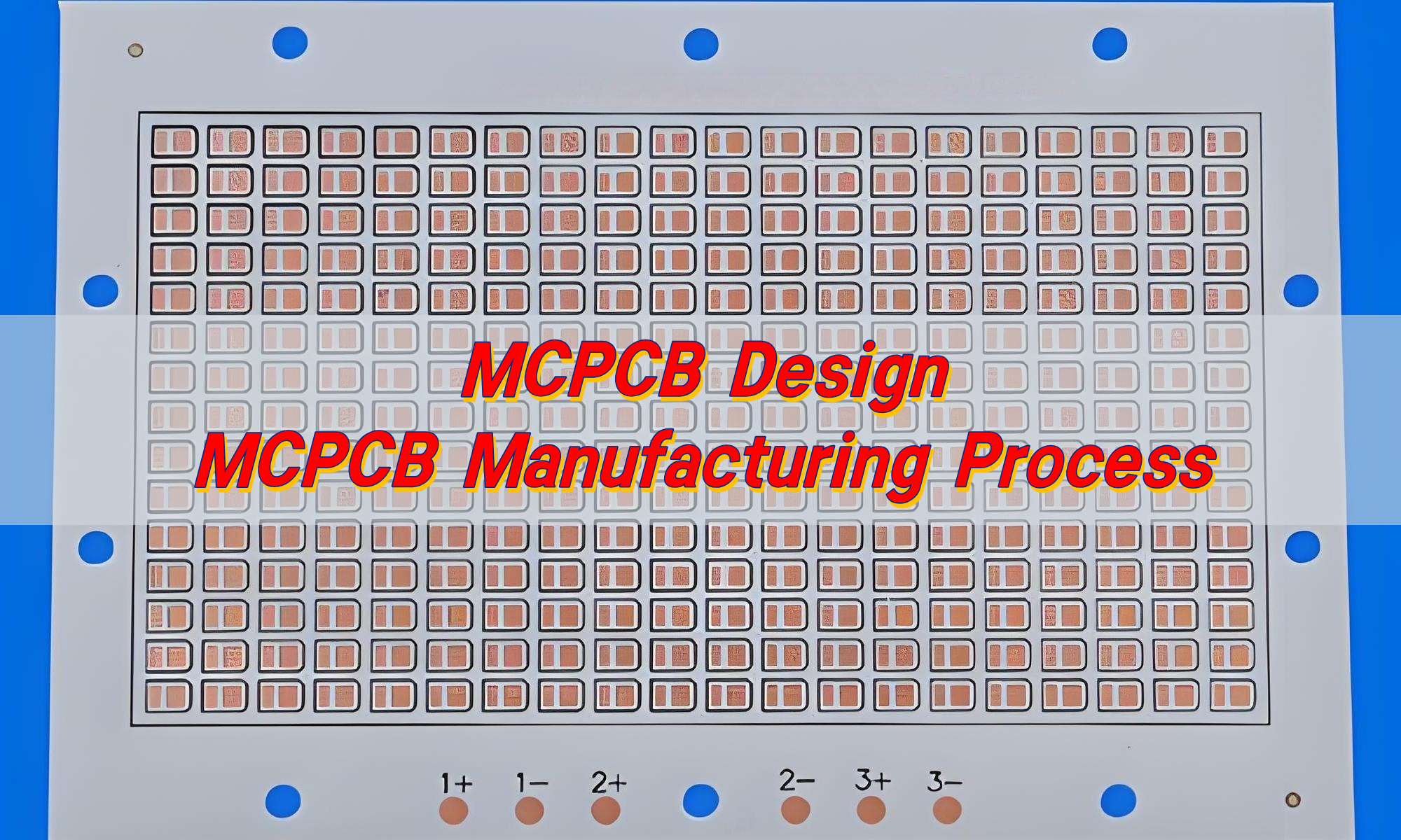
What is 12v MCPCB? Let’s discover its features, applications, benefits, design guide, production process and how to get a quote for 12v MCPCB.
Are you worried about these issues?
- Is your LED lamp’s lifespan frequently declining due to high temperatures? How can traditional PCBs overcome the thermal resistance bottleneck?
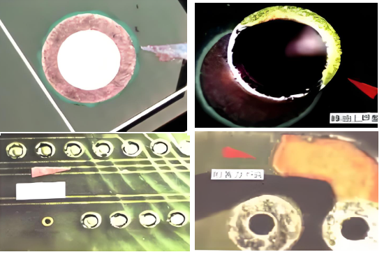
- In high-power 12V applications, are copper foil erosion and voltage drop issues significantly compromising your product’s stability?
- Can the supply chain provide a cost-effective solution while ensuring industrial-grade reliability and controlling BOM costs?
EBest Circuit (Best Technology) can provide solutions:
- Metal substrate + nano-thermal conductive layer: Using a 1.5mm aluminum substrate and a ceramic composite dielectric, thermal resistance is reduced by 40%, ensuring LED junction temperature ≤85°C.
- 4oz thick copper + laser micro-hole technology: Supports 20A continuous current, avoids local overheating through design-for-manufacturing optimization, and maintains voltage fluctuations below 3%.
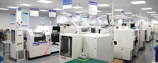
- Vertically integrated supply chain: From substrate to SMT, we manufacture the entire process in-house, reducing mass production costs by 30% and enabling fast delivery of small batches (starting in 7 days).
With 19 years of experience in metal substrates, we are not just a supplier, but your thermal management partner for high-reliability LED solutions. Contact us now if you have any request for 12v MCPCB: sales@bestpcbs.com.
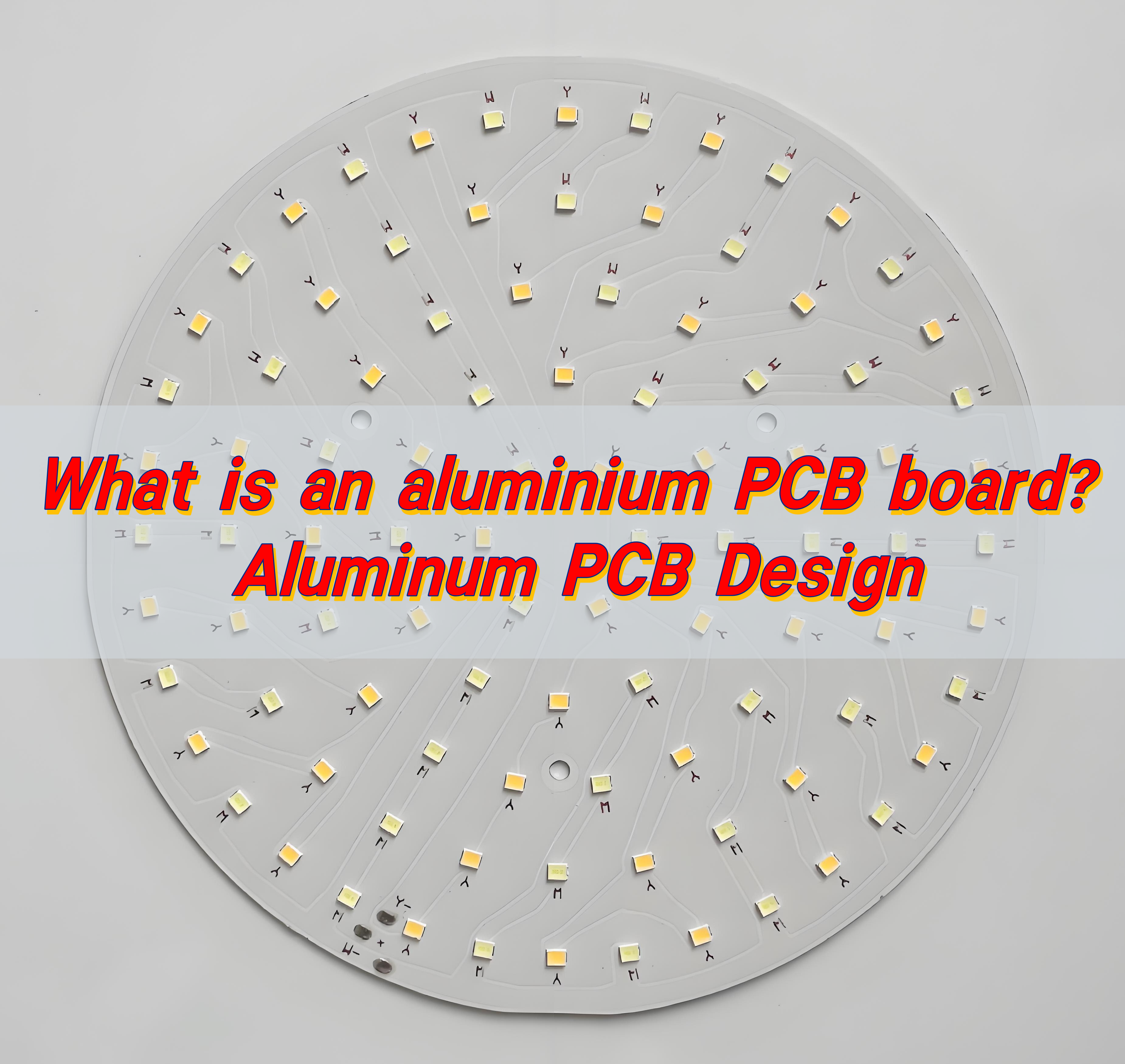
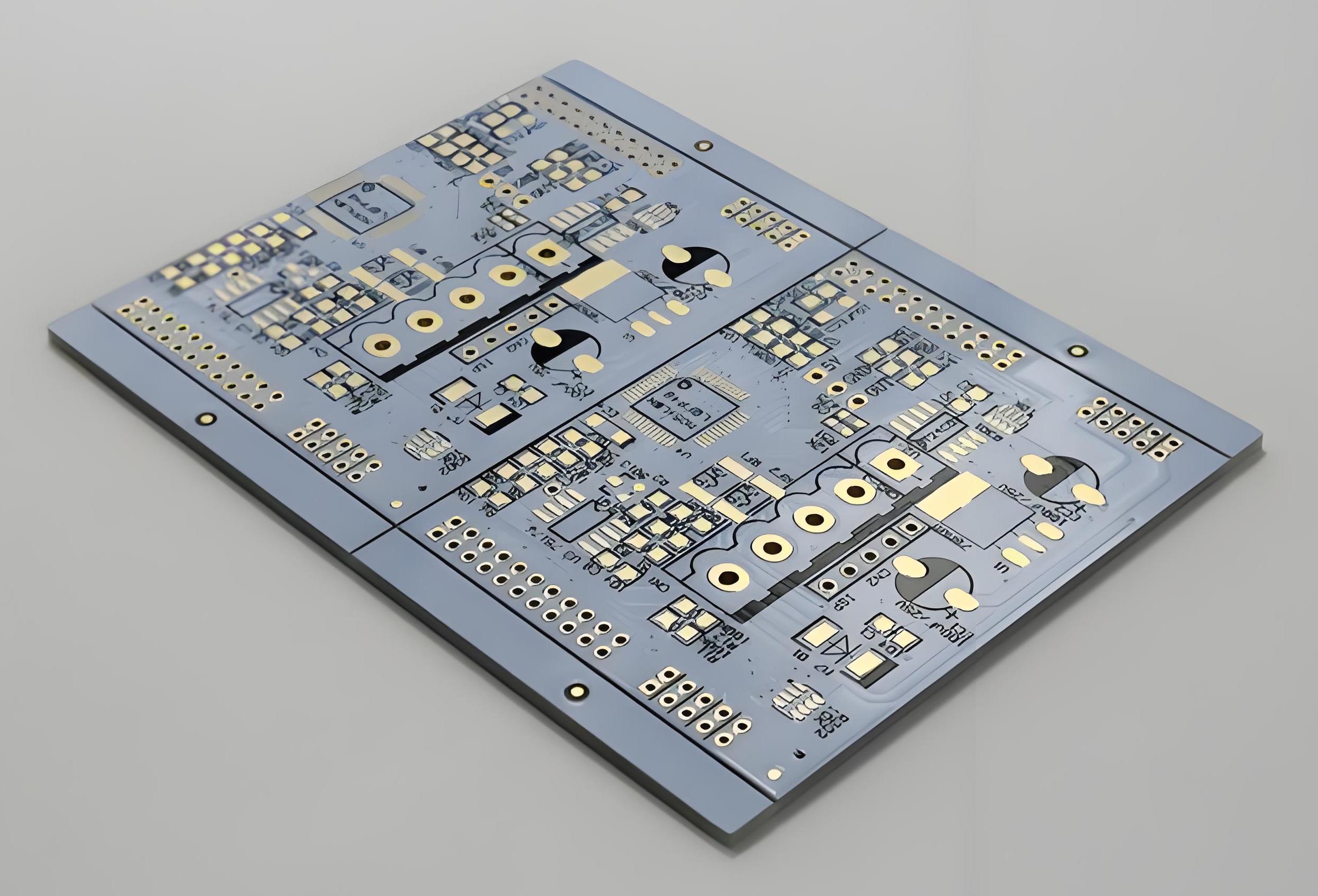
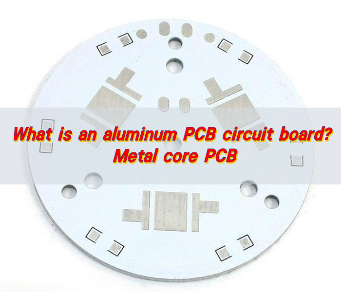
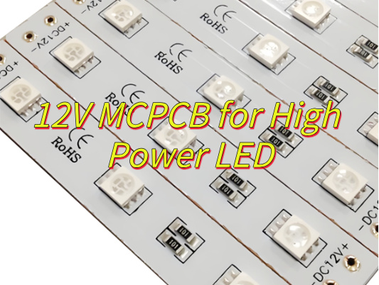
What Is a 12V MCPCB?
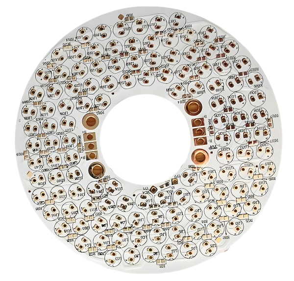
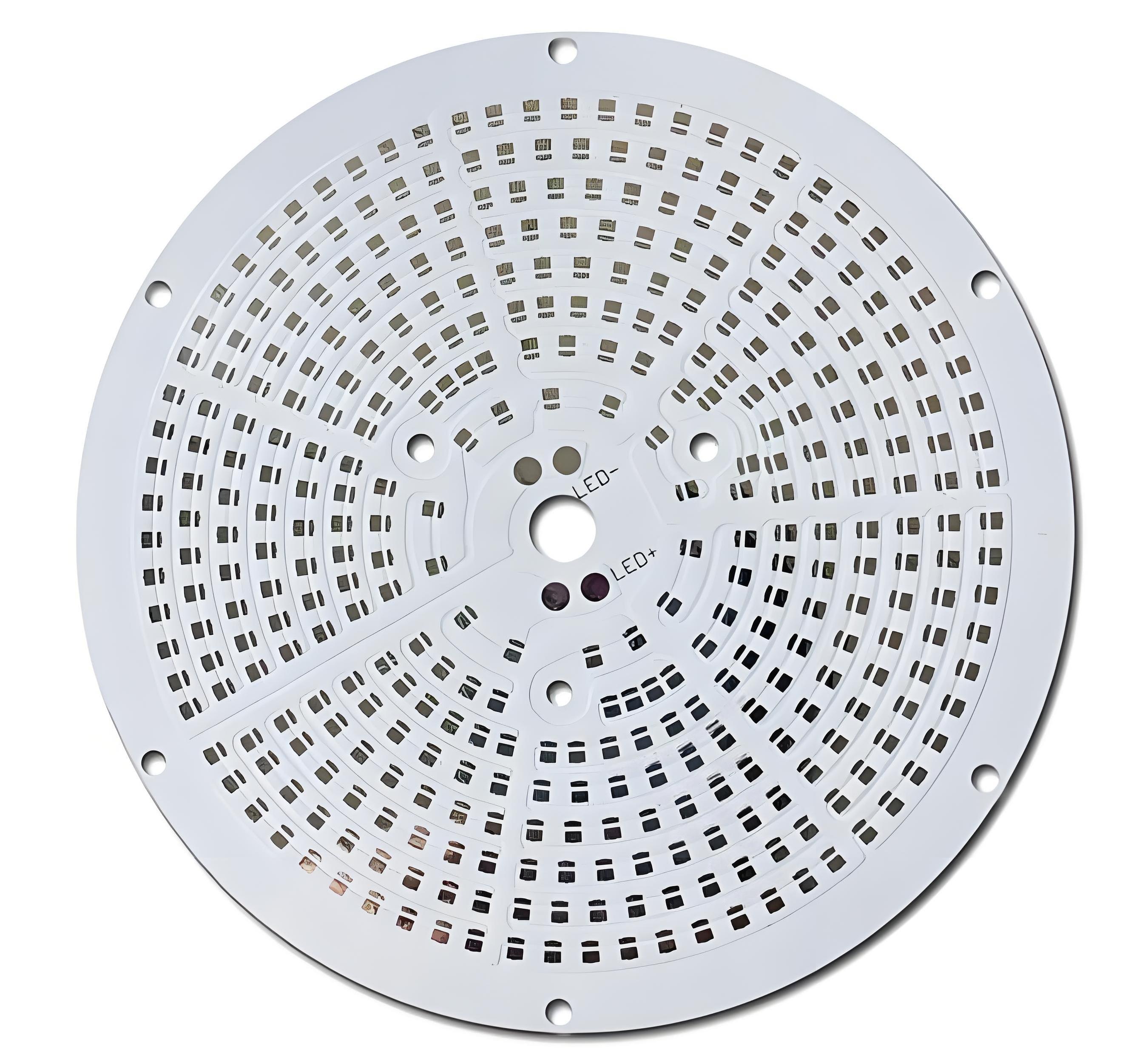
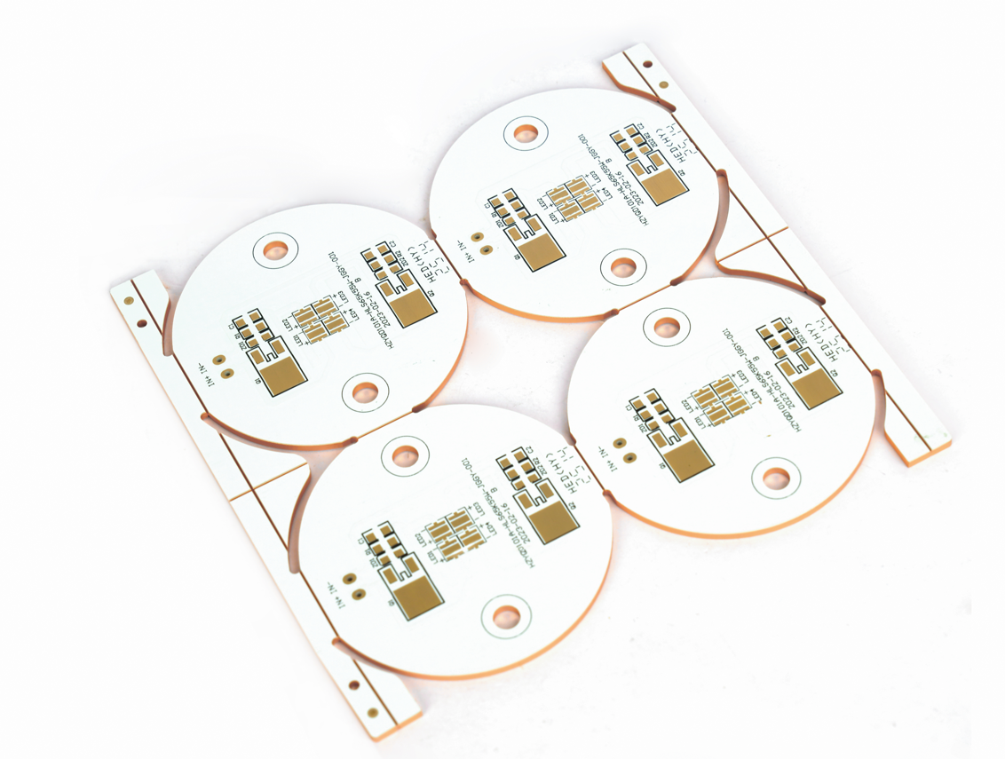
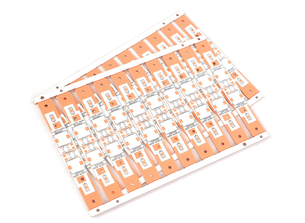
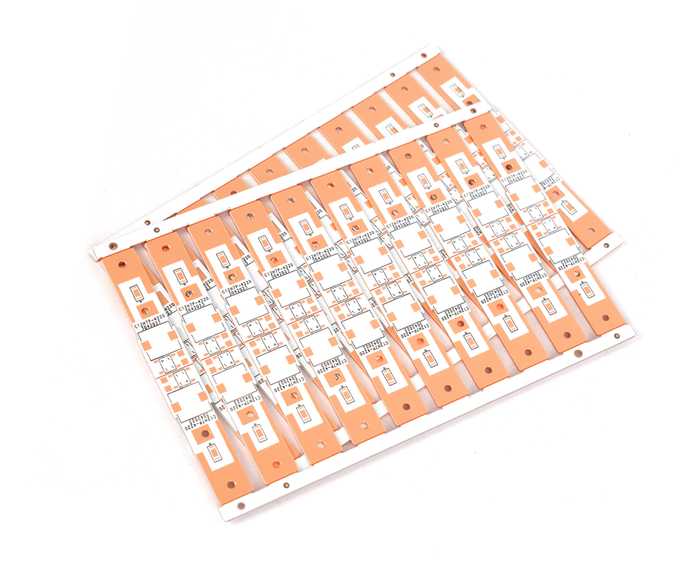
A 12V MCPCB (Metal Core Printed Circuit Board) is a specialized PCB using a metal substrate (e.g., aluminum or copper) as its core for efficient heat dissipation, designed to operate under 12-volt direct current (DC) systems. Its metal base layer rapidly conducts heat away from components, ensuring thermal stability and reliability. A 12V LED MCPCB specifically integrates this structure to support LED devices, combining 12V power compatibility with optimized thermal management for high-brightness or high-power LED applications.
What Are Features of 12V MCPCB?
- Voltage-Specific Design: Optimized for 12V DC systems, with trace widths and copper thicknesses (e.g., 2–3 oz) tailored to handle high current at low voltage.
- Enhanced Thermal Performance: Metal core (aluminum/copper) substrate with high thermal conductivity (2–38 W/m·K) rapidly dissipates heat, preventing thermal runaway in 12V power circuits.
- Thick Copper Traces: Heavy copper layers (≥2 oz) reduce resistive losses, enabling efficient current delivery for 12V LED drivers, motors, or power modules.
- Dielectric Insulation Layer: Specialized insulating material (e.g., epoxy-filled fiberglass) between metal core and copper traces ensures electrical isolation (≥500V breakdown voltage).
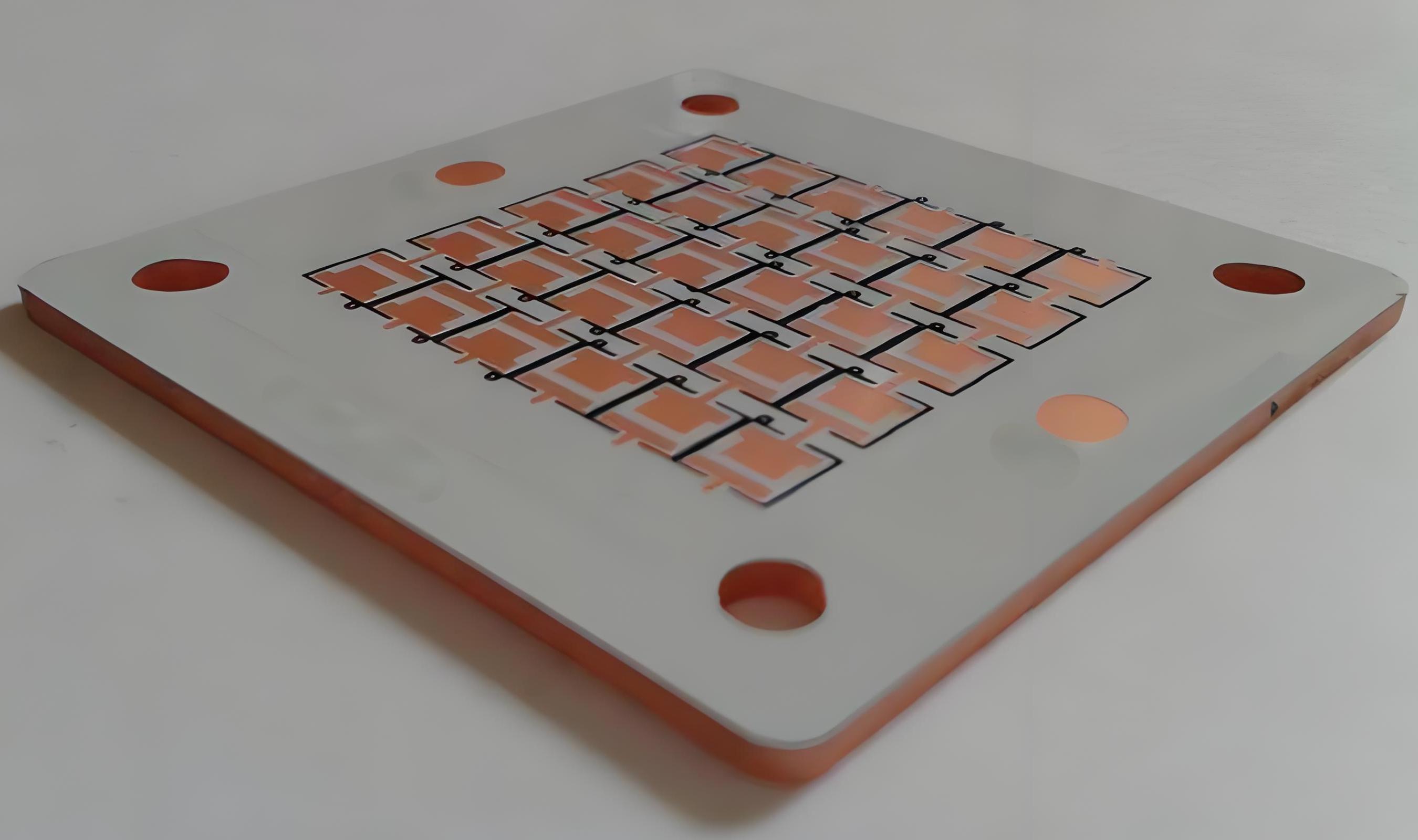
- Compact Layer Stackup: Typically 2-layer structure (signal + metal core) simplifies design for space-constrained 12V applications while maintaining mechanical rigidity.
- Thermal Stress Resistance: Metal substrate minimizes warping under thermal cycling, critical for 12V devices exposed to repeated heating/cooling (e.g., automotive LEDs).
- High-Current Trace Routing: Wide traces or copper pours accommodate 12V high-current paths (e.g., >5A) without excessive temperature rise.
What Are Applications of 12V MCPCB?
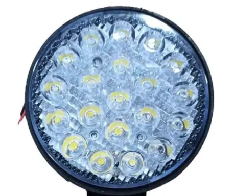
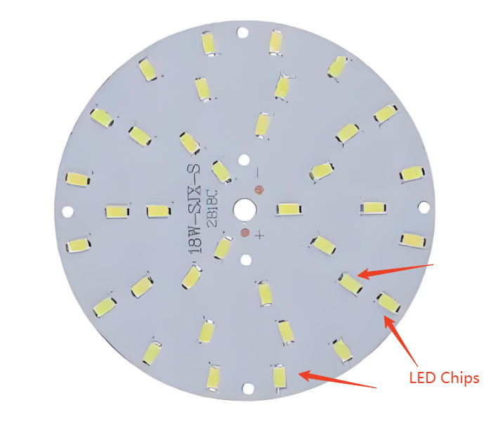
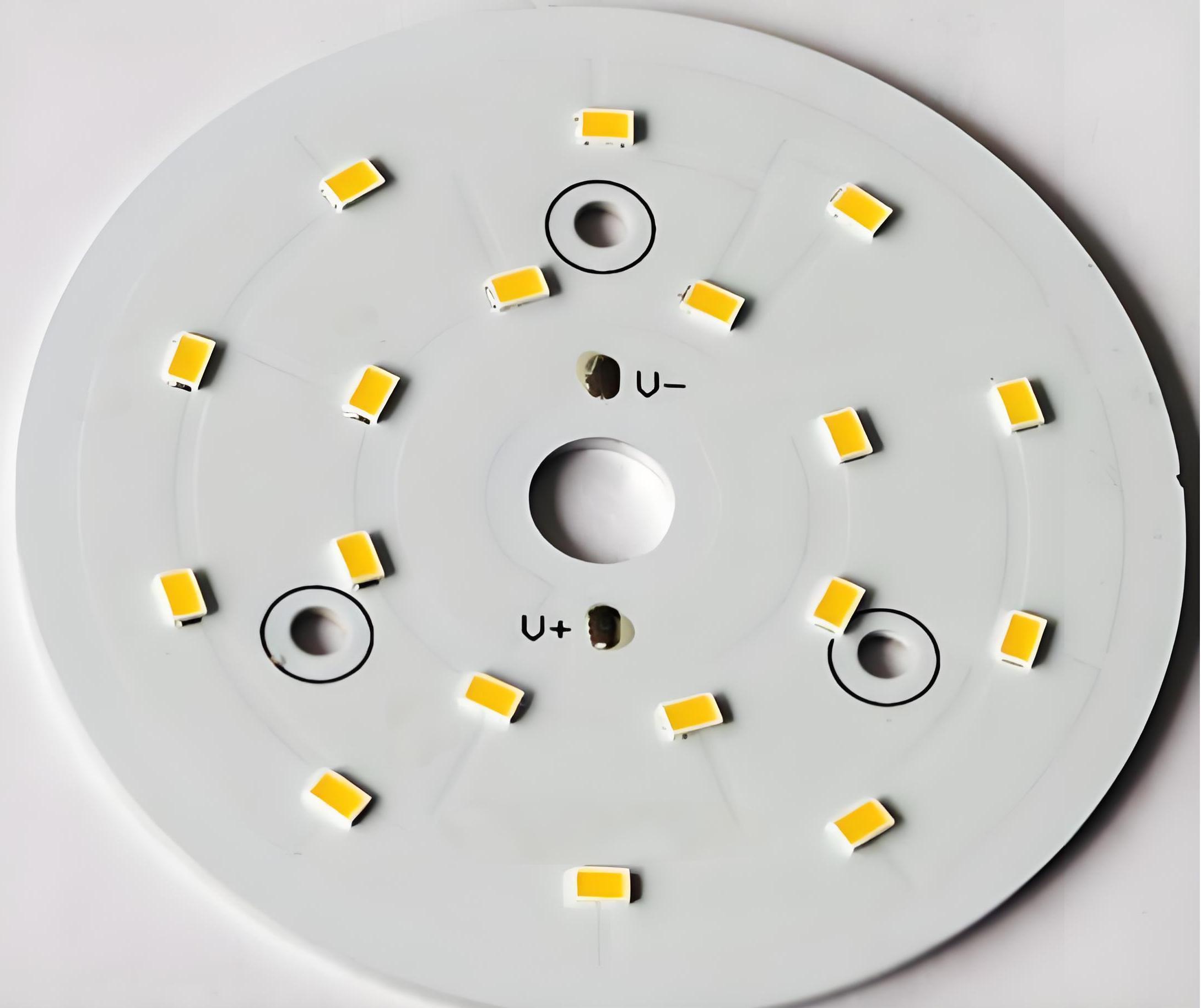
- LED Lighting Systems – Used in 12V LED strips, downlights, and streetlights, where metal-core PCBs efficiently dissipate heat from high-brightness LEDs, ensuring long lifespan and stable output.
- Automotive Electronics – Applied in 12V vehicle components (e.g., dashboard backlighting, interior/exterior LED lights, sensors) for vibration resistance and thermal management in harsh automotive environments.
- Power Conversion Modules – Integrated into 12V DC-DC converters, adapters, or battery chargers to handle high current with minimal heat buildup, enhancing reliability and efficiency.
- Industrial Control Equipment – Used in 12V motor drivers, PLC (Programmable Logic Controller) modules, or automation systems requiring compact, thermally robust PCBs for stable operation.
- Consumer Electronics Accessories – Found in 12V portable devices (e.g., power banks, USB hubs) to manage heat from power delivery components while maintaining compact form factors.
- Solar-Powered Lighting – Deployed in 12V solar streetlights or garden lamps, where MCPCBs ensure efficient heat dissipation for LEDs powered by solar batteries, improving system durability.
Why Choose 12V MCPCB for High Power LED?
Advantages of 12v MCPCB for high power LED:
- Superior Thermal Management: The aluminum/copper core rapidly dissipates heat, preventing LED performance degradation and extending lifespan.
- High Current Stability: Thick copper traces (35–280μm) ensure stable 12V power delivery, reducing voltage drops in high-power LED circuits.
- Enhanced Durability: Resists thermal cycling and mechanical stress, ideal for outdoor LED lighting and harsh environments.
- Energy Efficiency: Low thermal resistance minimizes energy loss, improving LED efficiency and reducing cooling costs.
- Compact Design: Enables slimmer LED modules compared to traditional PCBs, suitable for space-constrained applications.
- Long-Term Reliability: Prevents delamination and solder joint failures, ensuring consistent 12V LED performance over time.
- Customizable Solutions: Supports multi-layer designs and flexible shapes for diverse high-power LED configurations.
- Cost-Effective Maintenance: Reduces LED failure rates, lowering replacement and servicing costs in commercial/industrial setups.
How to Design A 12V MCPCB for High Power LED?
12V MCPCB Design Guide for High-Power LEDs
1. Define Requirements
- Confirm LED specifications (voltage, current, thermal resistance).
- Determine PCB dimensions and mounting method (e.g., heat sink compatibility).
2. Material Selection
- Choose aluminum-core substrate (1.5mm–3.2mm thickness) for heat dissipation.
- Use 2oz–4oz copper for traces to handle high currents.
- Select a dielectric layer (polyimide or ceramic-filled epoxy) rated for ≥12V.
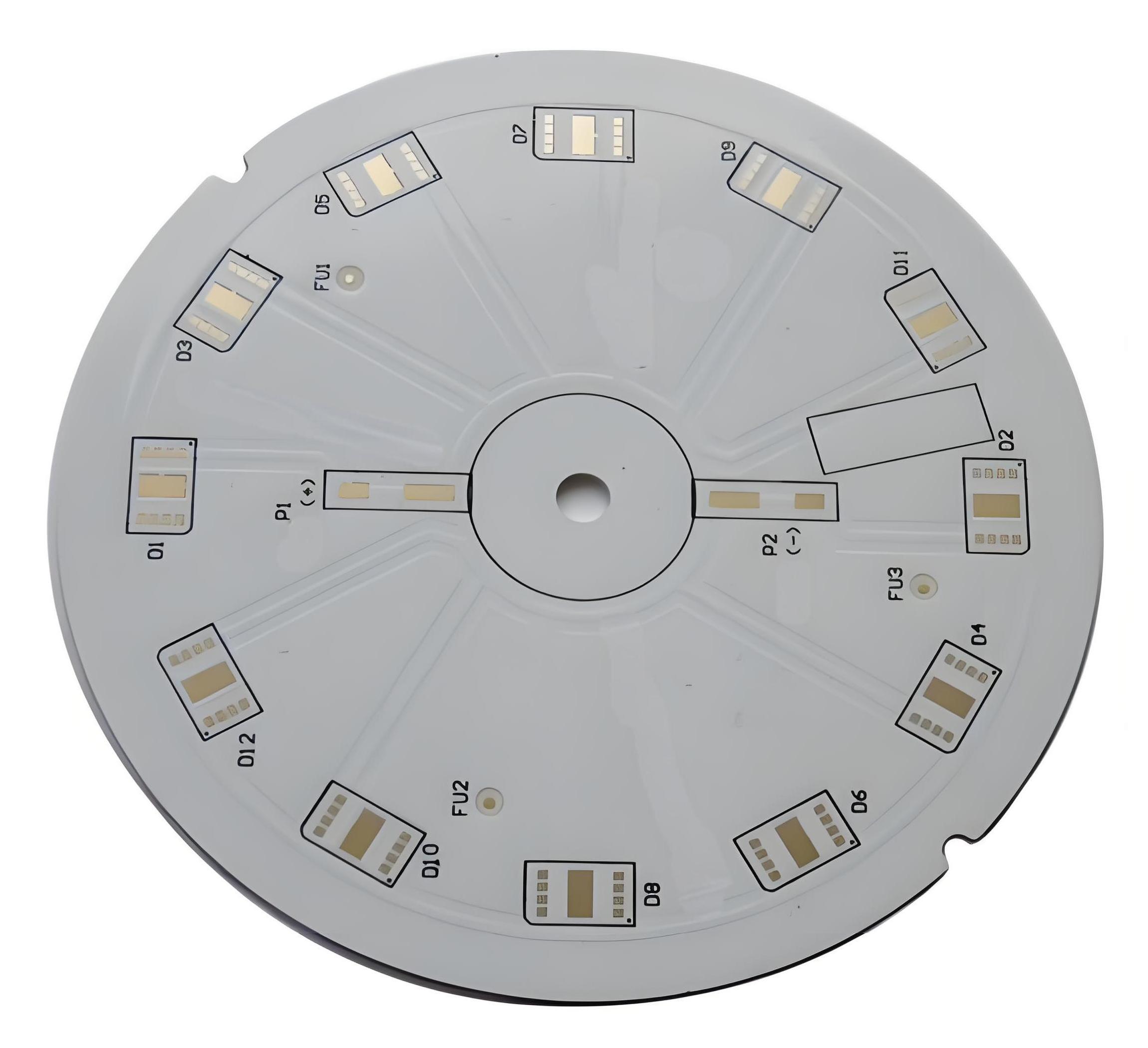
3. Circuit Layout
- Arrange LEDs in series to match 12V input.
- Design wide traces (≥2mm for 5A–10A) and minimize sharp bends.
- Place thermal vias (0.3mm–0.5mm diameter) beneath LED pads to conduct heat to the aluminum base.
4. Thermal Design
- Add a copper pour layer on the bottom PCB side, connected to thermal vias.
- Ensure dielectric layer thickness (50µm–100µm) balances insulation and heat transfer.
- Plan mounting holes for external heat sinks; use thermal interface material (TIM) between PCB and sink.
5. Manufacturing Preparation
- Apply solder mask to protect copper traces.
- Specify high-temperature solder (e.g., SAC305) for LED assembly.
- Maintain ≥0.2mm trace-to-trace clearance and ≥1mm dielectric edge margin.
6. Validation
- Test thermal performance using infrared imaging under maximum load (aim for ≤5°C rise above ambient).
- Verify voltage stability and trace current capacity.
- Run accelerated aging tests (e.g., 1000 hours at 85°C) to confirm long-term reliability.
7. Considerations
- Avoid overcrowding LEDs to prevent localized heating.
- Ensure thermal vias are evenly distributed under high-power components.
- Validate dielectric material compatibility with operating temperatures.
- Use PCB design tools (e.g., Altium, Eagle) for layout accuracy.
- Partner with manufacturers experienced in MCPCB fabrication for quality control.
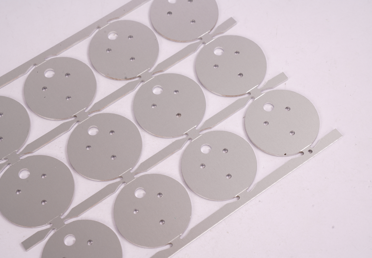
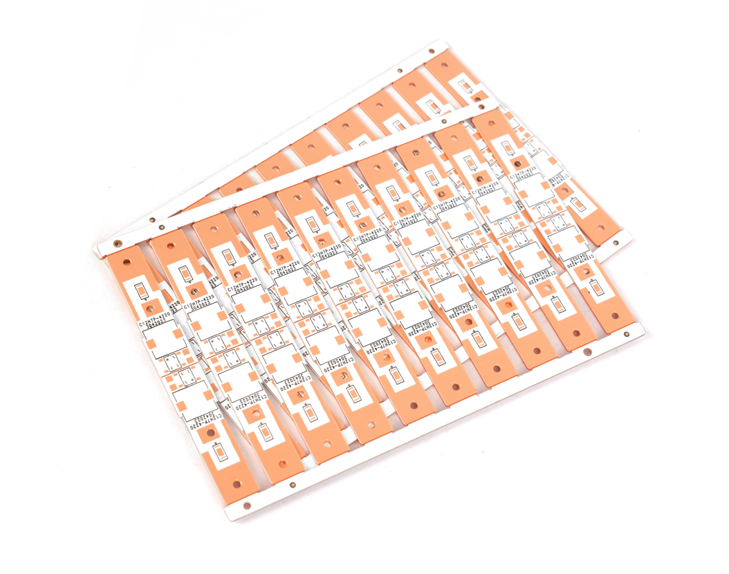
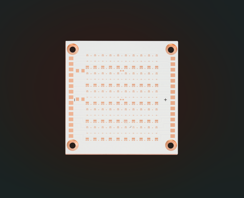
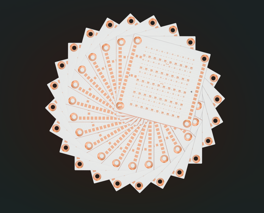
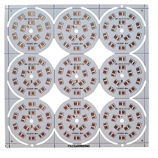
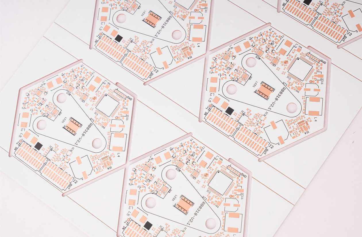
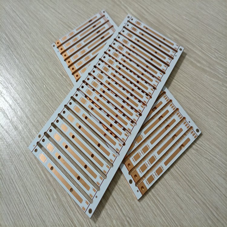
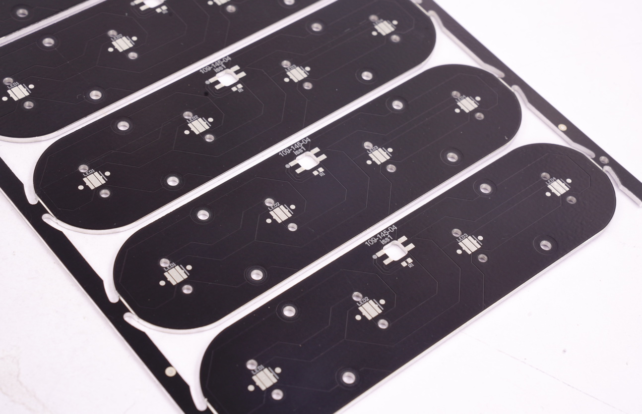
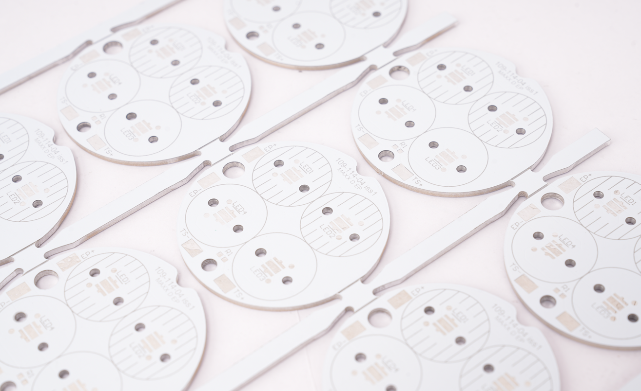
How to Make A 12V LED MCPCB?
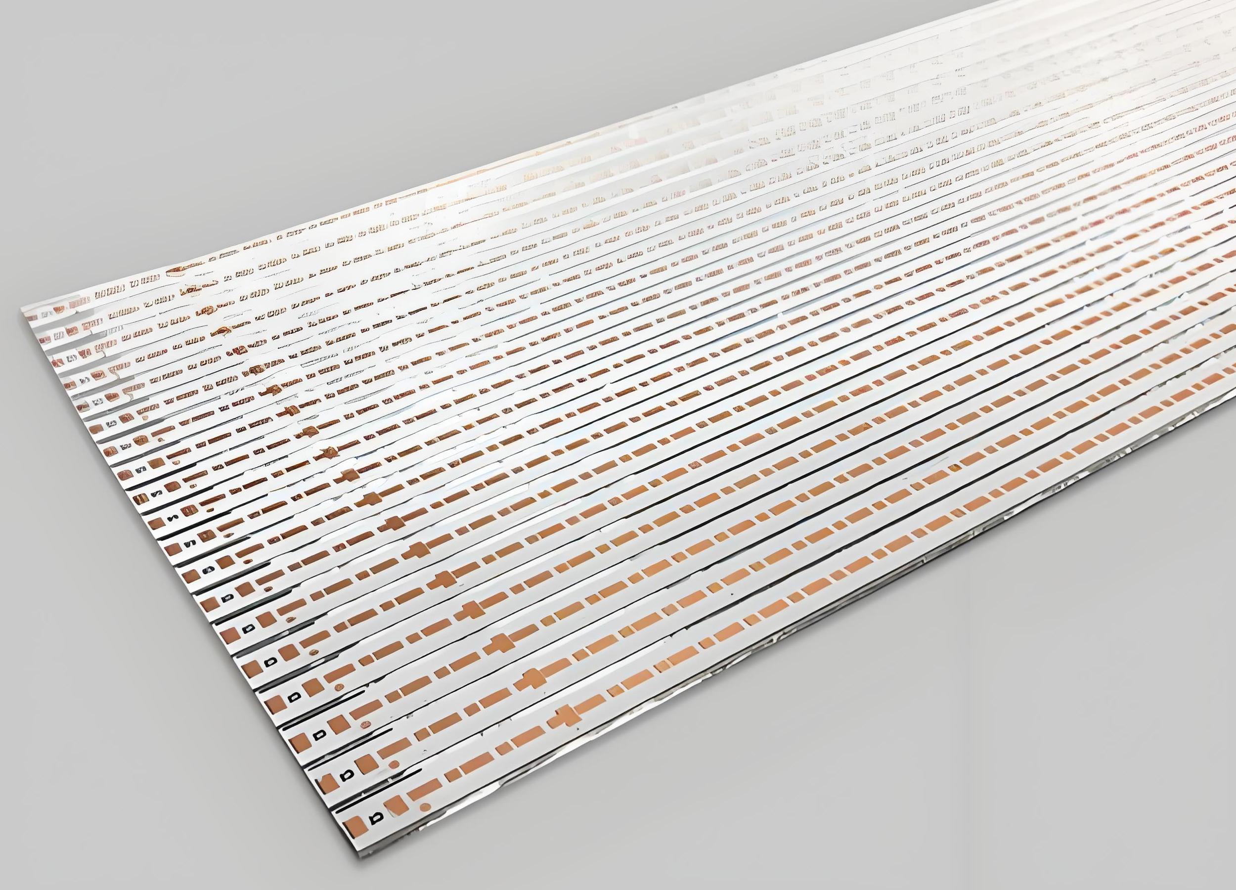
Production Process for 12V LED MCPCB
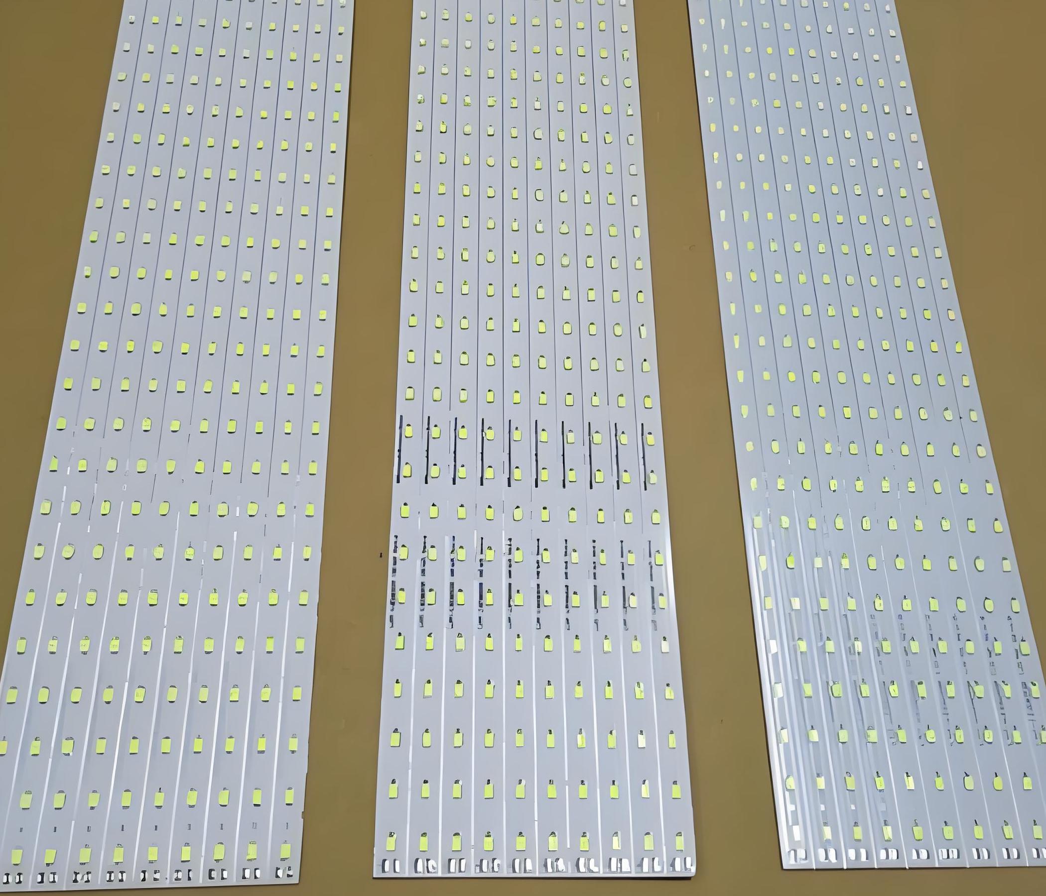
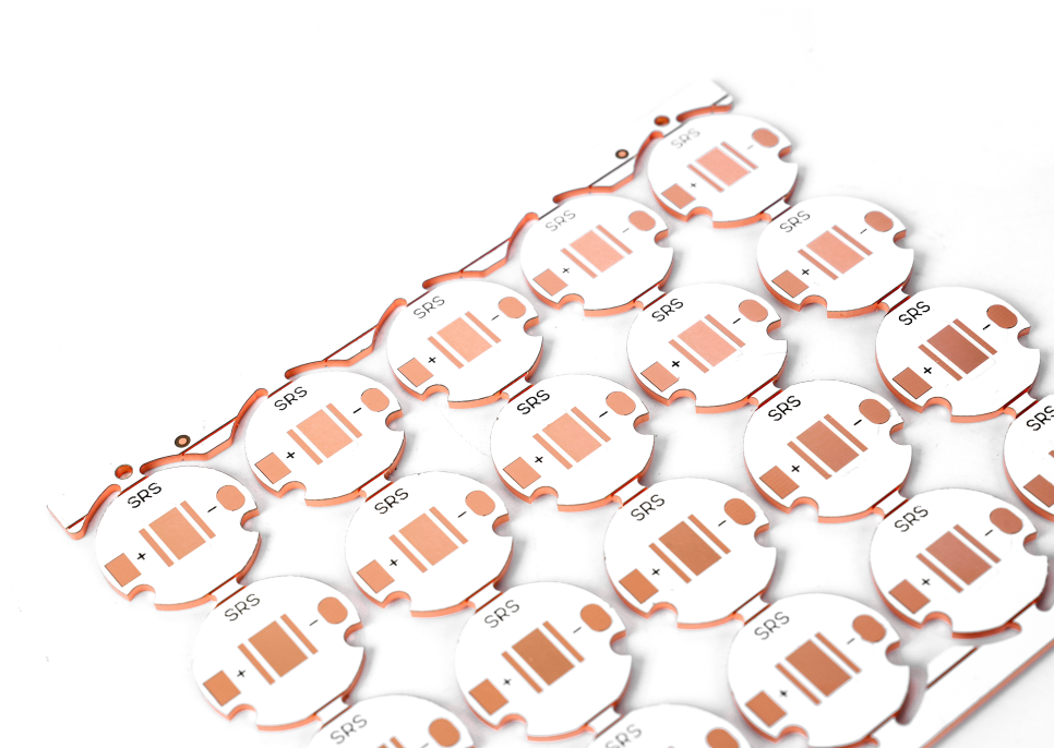
1. Material Preparation: Cut aluminum substrate (e.g., 5052/6061 series) to required dimensions. Clean surfaces to remove oils and impurities.
2. Drilling: Use CNC drills to create via holes and mounting holes. Ensure precision (e.g., ±50µm tolerance).
3. Dry Film Imaging & Etching: Apply dry film photoresist, expose to UV light through circuit patterns, and develop to retain copper traces. Chemically etch away excess copper, leaving only the designed circuitry.
4. Insulating Layer Deposition: Coat the aluminum base with a dielectric material (e.g., epoxy resin or ceramic-filled polymer) via screen printing.
5. Metallization: Deposit copper layers (1oz–4oz) on the insulating layer using electroplating or chemical sinking.
6. Surface Finish: Apply surface treatments like HASL (spray tin), ENIG (immersion gold), or OSP (organic solderability preservative) for solderability.
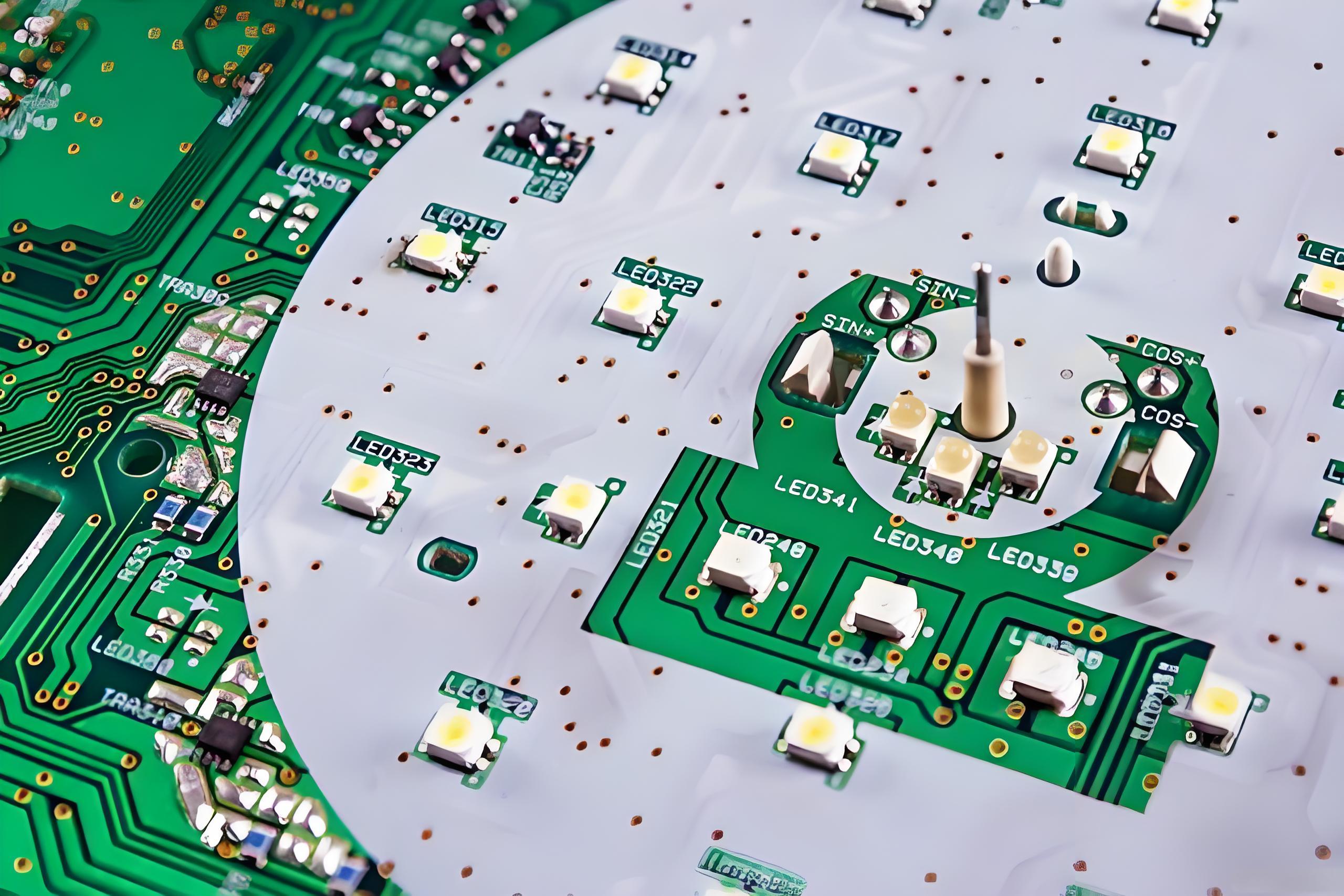
7. Component Assembly: Use SMT (Surface Mount Technology) to place LEDs, resistors, and other components. Reflow solder in a controlled oven.
8. Testing & Inspection: Perform electrical tests (continuity, voltage drop) and thermal imaging (≤5°C rise above ambient). Conduct AOI (Automated Optical Inspection) for defects like shorts or misalignment.
9. Packaging: Vacuum-seal finished boards with desiccant packs. Include test reports and label specifications.
Why Choose EBest Circuit (Best Technology) as LED MCPCB Manufacturer?
- 19+ Years Industry Experience: Leverages proven expertise to navigate complex high power LED applications.
- Stringent Quality Certifications (ISO9001, ISO13485, and IATF16949): Ensures product consistency and compliance with global standards.
- Advanced Thermal Management Solutions: Prevents LED overheating, extending product lifespan and reliability.
- Competitive Pricing: No Hidden Cost. Affordable pricing without compromising quality, ideal for cost-sensitive projects.
- 24 Hours Rapid Prototyping: Accelerates time-to-market, meeting urgent production demands.
- Free DFM (Design for Manufacturability) Service: Identifies design flaws early, reducing rework costs and delays.
- Advanced Quality Control – 100% automated optical inspection (AOI) and X-ray testing for defect-free boards.
- Reliable Supply Chain – Stable material sourcing to avoid delays and ensure consistency.
- One-Stop Solution – From prototyping to mass production, we handle all stages seamlessly.
- Dedicated Customer Service – 24/7 technical support for real-time project tracking and issue resolution.
How to Get A Quote For LED MCPCB Project?
Essential Information for Accurate Quotation
1. Design Files:
- Gerber/ODB++ files, Bill of Materials (BOM), and 3D mechanical drawings.
2. Technical Specs:
- LED type (e.g., Cree XP-G3, Samsung LH351H) and power rating.
- Circuit voltage (12V/24V) and current requirements.
- Thermal constraints (max operating temperature, heat sink compatibility).
3. Material Preferences:
- Substrate type (aluminum, copper, or ceramic).
- Copper thickness (1oz–4oz) and surface finish (HASL, ENIG, OSP).
4. Production Details:
- Order quantity (prototype/mass production).
- Lead time expectations.
- Certification requirements (RoHS, UL, ISO).
Ready to quote?
Contact us now and submit your requirements to sales@bestpcbs.com!