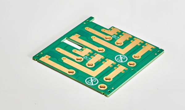
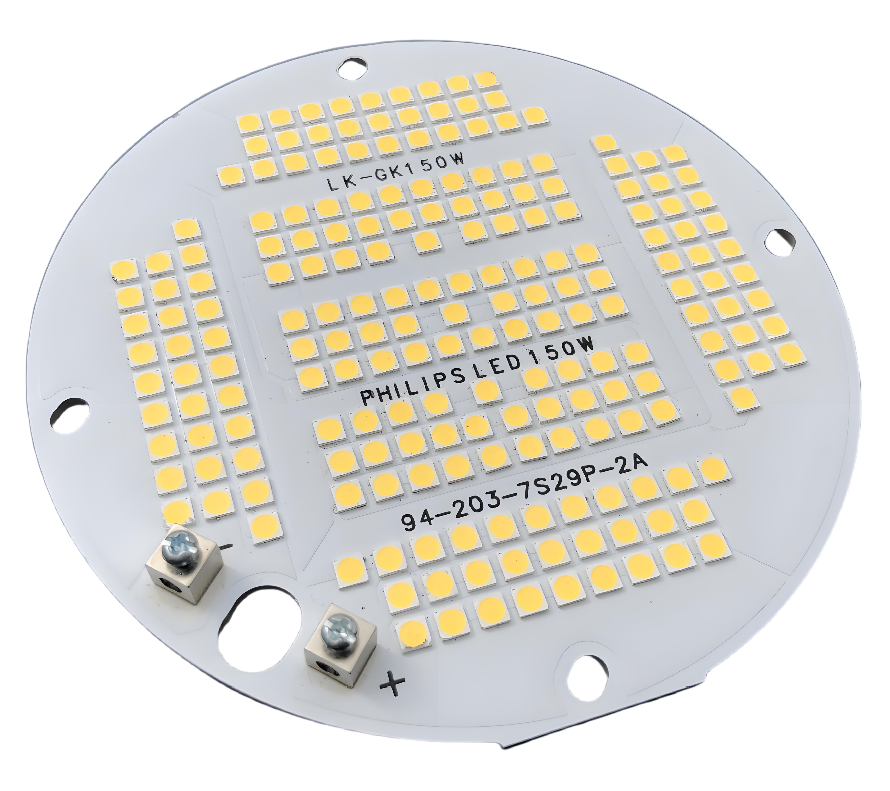
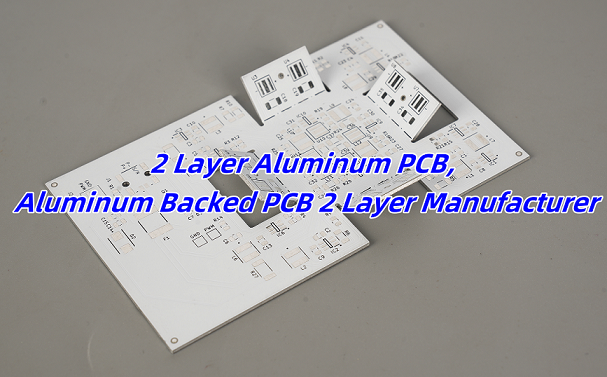
What is a 2 Layer Aluminum PCB?
A 2 layer aluminum PCB is a high-performance metal core PCB (MCPCB) designed for applications where heat dissipation and mechanical strength are critical. Unlike FR4-based PCBs, which rely on fiberglass as the core, aluminum PCBs use an aluminum alloy base to improve heat transfer and enhance mechanical support.
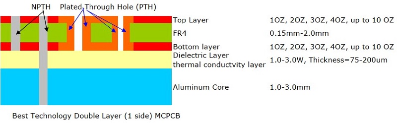
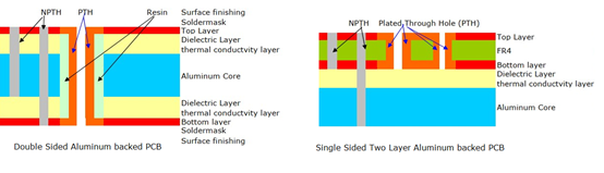
In a 2-layer aluminum PCB, two copper layers are stacked on top of a dielectric layer, which is then bonded to the aluminum substrate. Different with double sided aluminum PCB, the two copper trace layers of 2 layer aluminum PCB are on the one side, there is only one side enable to mount components.
Key Features of a 2-Layer Aluminum PCB:
- Aluminum core for structural support & stable dimensions
- Two copper layers for improved conductivity
- Dielectric layers for electrical insulation
- Efficient heat dissipation to prevent overheating
What Are the Layers of a 2 Layer Aluminum PCB?
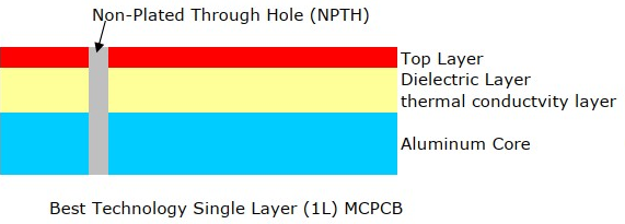
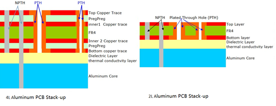
A 2 layer aluminum PCB is constructed with the following layers:
- Copper layer 1 (top layer) – The top conductive layer, where surface-mount components are placed.
- FR4 material – Provides electrical insulation while allowing heat dissipation to the next layer.
- Copper layer 2 (bottom layer) – The second conductive layer, allowing for more complex routing compared to single-layer designs.
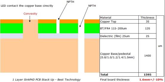
- Dielectric layer (thermal conductivity layer) – Filled with dielectric material, aiming to further insulates the second copper layer from the aluminum core.
- Aluminum Base – A metal core that improves heat dissipation and mechanical durability. Commonly made of 6061, 5052, or 1060-grade aluminum
Additional layers, such as a solder mask and silkscreen, are often applied onto the top copper layer for protection and labeling.
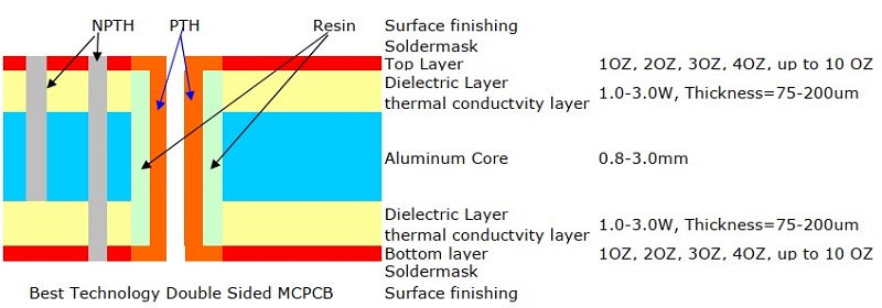
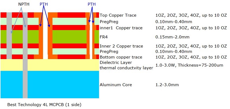
4 vs 2 Layer Aluminum PCB Stack up
A 4-layer aluminum PCB adds more conductive layers to support higher circuit complexity, but it also increases manufacturing costs and thickness. They have different stack ups, but the layers construction is the same, see the stack ups as following:
Advantages & Disadvantages of Aluminum PCB
- Advantages:
✅ Excellent Heat Dissipation – Aluminum conducts heat 8–9 times better than FR4, reducing thermal stress and preventing higher thermal damage to the components.
✅ Better Mechanical Strength – Due to its metal base, it is more durable than traditional PCBs, resistant to bending and cracking.
✅ Higher Circuit Density – Two stacked copper layers allow for more intricate circuit designs.
✅ Reduced PCB Size and Money Saving – Since heat dissipation is built-in, external heat sinks are often not needed, reducing the overall circuit footprint.
✅ Lower Thermal Expansion – Aluminum base has stable dimension and lower thermal expansion, prevents warping or deformation under high temperatures.
✅ Lightweight – Lighter than copper-based PCBs, it is suitable for those weight sensitive projects, such as automotives.
✅ Eco-Friendly – Aluminum is recyclable, making it a greener choice.
- Disadvantages:
❌ Higher Cost – More expensive than FR4 PCBs due to complex manufacturing.
❌ Limited Multilayer Options – Aluminum PCBs typically do not exceed 4 layers, unlike FR4, which can have up to 40 layers.
What is the Difference Between FR4 and Aluminum PCB?
When our sales talking with customers, there is always be mentioned that what are the differences between normal FR4 pcb and aluminum PCB? Most of them in the design consultation stage are not sure which circuit board is more suitable for their needs. Today, to give more engineers a clear understanding, Best Team listing the different characteristics and parameters between them, hope it is easy to make you sense.
| Feature | FR4 PCB | Aluminum PCB |
| Core Material | Fiberglass (FR4) | Aluminum Metal Base |
| Thermal Conductivity | 0.3 – 0.4 W/m·K | 1.0 – 3.0 W/m·K |
| Heat Dissipation | Requires external heat sinks | Direct heat dissipation |
| Mechanical Strength | Moderate | High (resistant to bending) |
| Weight | Lightweight | Slightly heavier, but lighter than copper-based PCB |
| Electrical Insulation | High | Lower (requires dielectric layer) |
| Manufacturing Cost (under the same design) | Lower | Higher |
| Maximum Layers | Up to 100 layers | Typically 1 – 4 layers |
| Flexibility | Can be rigid or flexible | Can be rigid and semi-flexible (use special technique) |
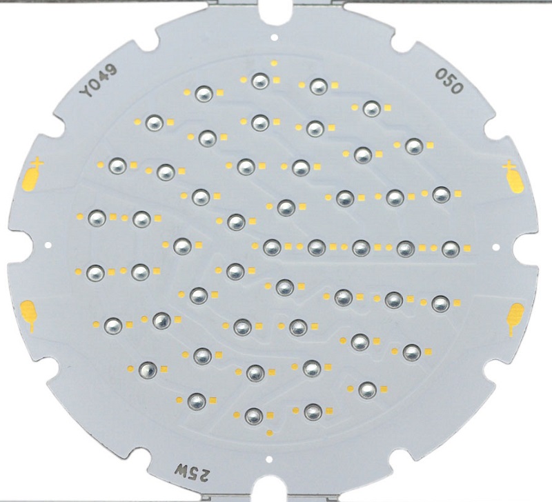
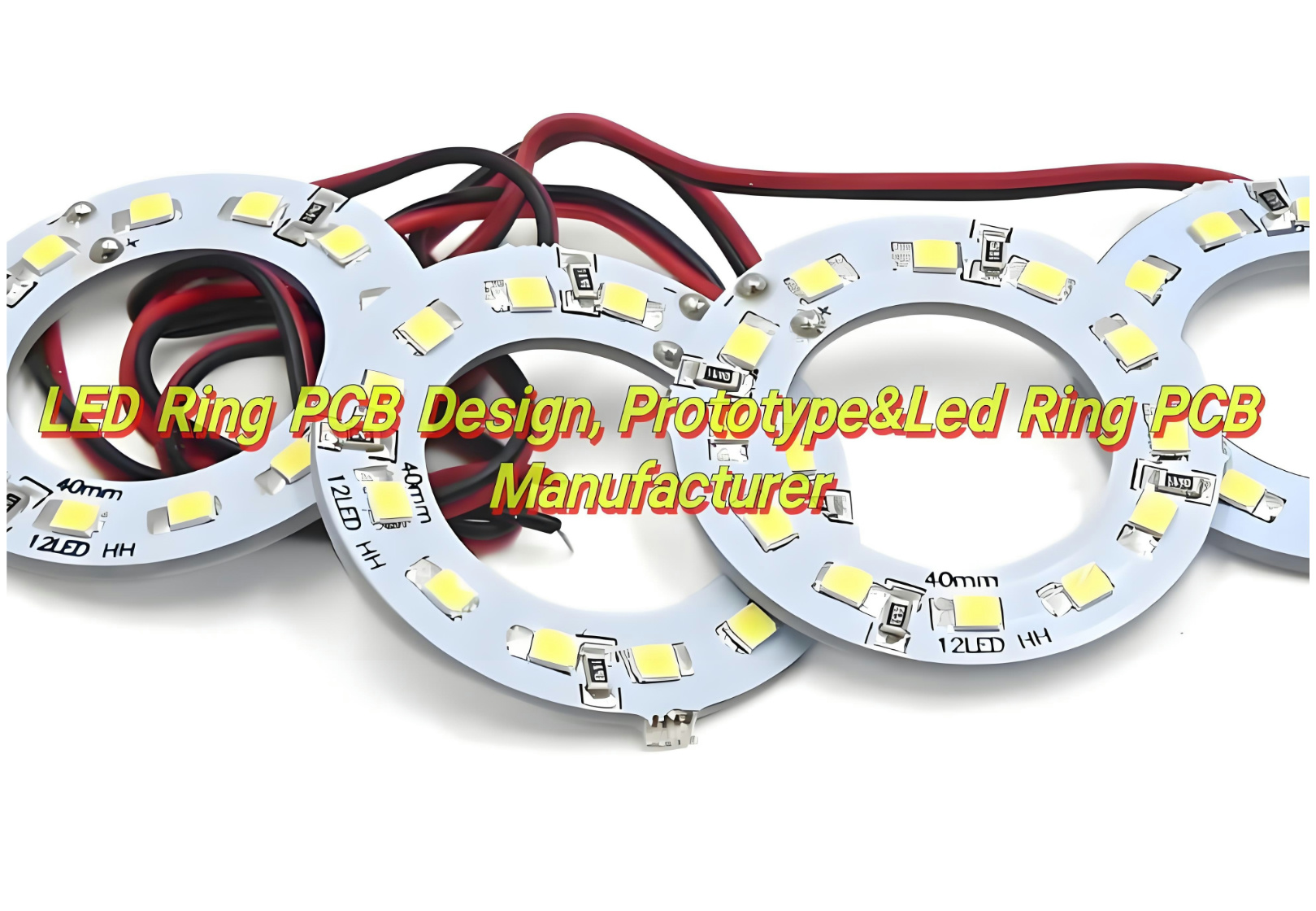
| Applications | Consumer electronics, computing… | Mainly in LEDl lightings |
| Durability | Less resistant to thermal expansion | High thermal stability |
How Thick is the Dielectric Layer of an 2 Layer Aluminum PCB?
As we know, a thinner dielectric layer offers better heat transfer, but lower insulation resistance. Normally, the dielectric layer used in a 2-layer aluminum PCB typically ranges between 75µm to 200µm. Each has its different thermal conductivity, choosing the right thickness depends on current requirements and operating conditions.
| Dielectric Thickness (mm) | Thermal Conductivity (W/m·K) | Common Application |
| 0.075 mm (75µm) | 1.0 – 1.5 | Low-power circuits |
| 0.1 mm (100µm) | 2.0 – 3.0 | LED lighting, power modules |
| 0.15 mm (150µm) | 3.0 – 5.0 | High-power applications |
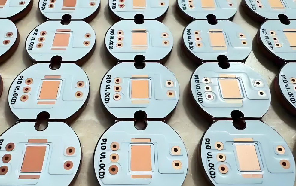
How to Make a 2 Layer Aluminum PCB?
The manufacturing process of a 2 layer aluminum PCB is different from standard FR4 PCBs due to the presence of a metal core. The following steps detail the fabrication process, show how EBest Circuit (Best Technology) manufacture the 2 layer aluminum PCB:
1. Material Selection
Choosing high-quality materials is the foundation of a reliable 2 layer aluminum PCB.
- Aluminum Core: Typically 6061, 5052, or 1060-grade aluminum, offering high thermal conductivity and mechanical strength.
- Copper Foil: 1 oz to 4 oz copper thickness, depending on current-carrying requirements.
- Dielectric Layer: 75um-200um, depends on the project demand.
2. Manufacture a Double Sided FR4 PCB
Manufacture a double sided FR4 PCB according to the files. Both top and bottom copper traces are plated into the required thickness.
3. Laminate the Dielectric Layer
A dielectric layer is added between the aluminum base and the FR4 PCB, then laminate them into a whole product. The thickness of this layer varies from 0.075 mm to 0.15 mm, depending on the thermal performance required.
4. Circuit Patterning (Imaging & Etching)
- A photosensitive dry film is applied to define circuit traces.
- UV exposure and development create the desired circuit pattern.
- An etching process removes unnecessary copper, leaving behind precise circuit traces.
5. Drilling & Plating
- Precision drilling creates vias and mounting holes.
- A plating process is used to form electrically conductive vias, connecting the top and bottom copper layers.
- The aluminum base is not conductive, so plated through-holes (PTHs) require special insulation to prevent electrical shorts.
6. Solder Mask & Silkscreen
- A protective solder mask is applied to prevent oxidation and improve insulation.
- Silkscreen printing is added for component labeling and identification.
7. Surface Finish Application
The surface finish ensures solderability and prevents oxidation. Common options include:
- HASL (Hot Air Solder Leveling) – Cost-effective but not ideal for fine-pitch components.
- ENIG (Electroless Nickel Immersion Gold) – Provides a smooth, corrosion-resistant surface.
- OSP (Organic Solderability Preservative) – Environmentally friendly and cost-efficient.
8. Testing & Quality Inspection
- Automated Optical Inspection (AOI) verifies circuit accuracy.
- Electrical testing ensures there are no open circuits or shorts.
- Thermal testing checks heat dissipation performance.
Once the PCB passes inspection, it is ready for component assembly or shipping to customers. Here is a manufacturing process video of aluminum, hope this is easy for you to understand.
Differences Between 6061, 5052, and 1060 Aluminum Alloy
When manufacturing a 2 layer aluminum PCB, selecting the right aluminum alloy is essential for achieving the desired thermal conductivity, mechanical strength, and corrosion resistance. The three most common aluminum alloys used in PCBs are 6061, 5052, and 1060, each offering different properties suitable for various applications.
| Property | 6061 Aluminum | 5052 Aluminum | 1060 Aluminum |
| Composition | Al-Mg-Si alloy | Al-Mg alloy | High-purity aluminum (≥99.6%) |
| Thermal Conductivity | 150 – 170 W/m·K | 138 – 147 W/m·K | 230 – 237 W/m·K |
| Mechanical Strength | High (275 – 310 MPa tensile strength) | Moderate (190 – 240 MPa tensile strength) | Low (60 – 100 MPa tensile strength) |
| Corrosion Resistance | Moderate | High (excellent saltwater resistance) | Low (prone to corrosion) |
| Workability | Good machinability, harder to bend | Easy to form and bend | Very soft, easy to process |
| Cost | Higher | Moderate | Lower |
- For high-power applications (e.g., power amplifiers, automotive circuits): 6061 is ideal due to its strength.
- For outdoor or humid environments (e.g., industrial lighting, marine electronics): 5052 offers the best balance.
- For cost-effective, high-thermal applications (e.g., LED lighting, heat-sensitive electronics): 1060 is the best choice.
At EBest Circuit (Best Technology), we have various aluminum base in our storage, whatever you want to use 6061, 5052 or 1060, we can meet your requirements. As a reliable 2-4 layer metal core pcb (mcpcb) aluminum manufacturer, we specialize in custom aluminum-backed PCBs, ensuring high quality, competitive pricing, and fast turnaround times. Whether you need prototyping or mass production, our engineering team is ready to assist you. Contact us right now to get your quotation!