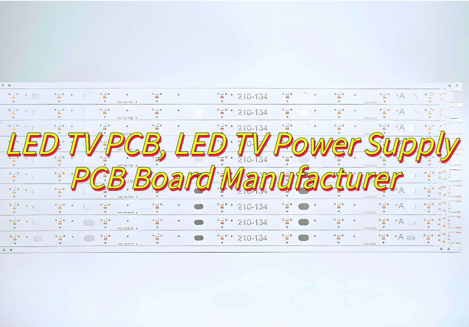
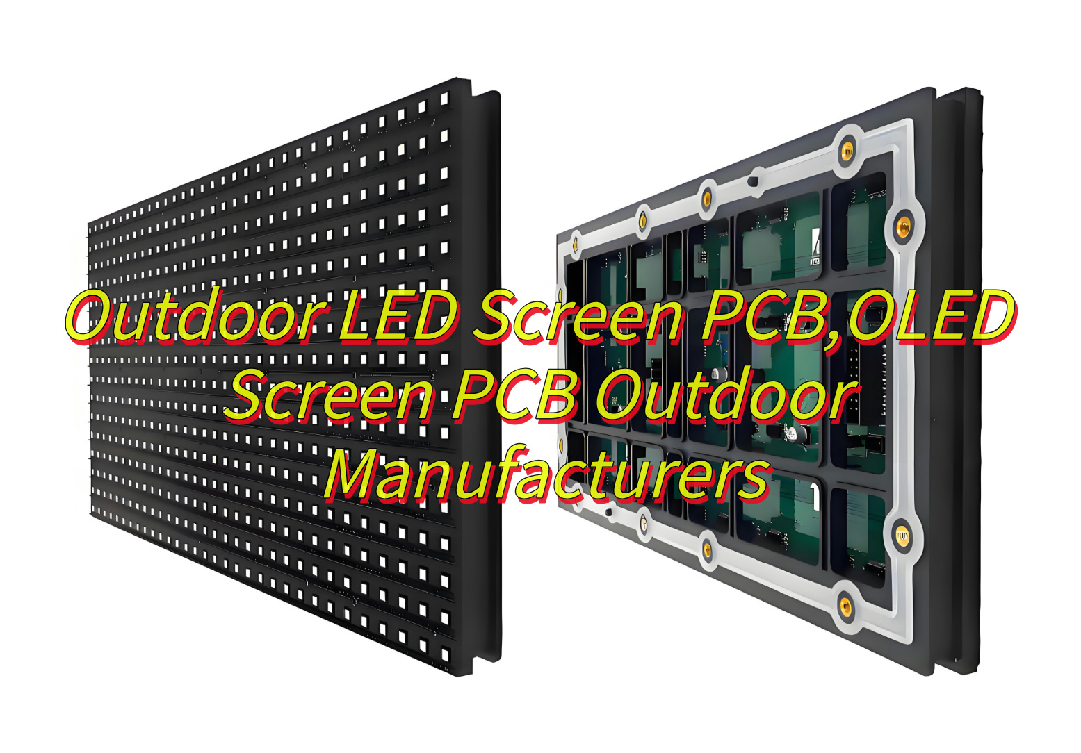
In the rapidly evolving world of electronics and lighting, the demand for custom LED PCB is climbing fast. Whether you’re building industrial lights, consumer gadgets, or smart wearables, choosing a dependable LED PCB manufacturer can set your project apart in terms of quality, efficiency, and performance.
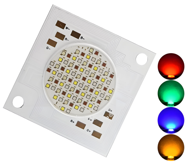
If you’re looking for high-performance lighting solutions with reliable circuitry, you need more than just a product. You need a trusted partner. EBest Circuit (Best Technology) is that partner. We are a leading LED PCB manufacturer with over 18 years of hands-on experience. We specialize in crafting custom LED PCB solutions that go beyond ordinary lighting components. Our team supports industries ranging from automotive and aerospace to medical and consumer electronics. Whether you need a DIY LED PCB board, SMD LED PCB board, or help with LED PCB board replacement, we offer unmatched quality, guidance, and long-term value.
What Is a Custom LED PCB?
What is a custom LED PCB? A custom LED PCB is a printed circuit board designed to support and connect light-emitting diodes in a specific configuration. Unlike off-the-shelf boards, these are tailored to fit your product’s shape, power needs, and environmental demands.
Whether it’s a curved light strip, a compact torch design, or a large-format display backlight, a custom LED PCB meets your unique criteria with pinpoint accuracy. It’s not just about making it fit—it’s about optimizing performance.
Why Customization Matters in LED PCB Design?
Every application has different priorities. Some need intense brightness. Others demand heat control in confined spaces. A few require flexible materials or rigid aluminum cores. A standard LED PCB board simply can’t’ cater to all these needs.
With custom LED PCB design, you have full control over:
- LED type and layout
- Trace width and thickness
- Copper weight
- Heat dissipation paths
- Voltage and current specifications
- Mounting hole placements
- Base material selection
What Services Does EBest Circuit (Best Technology) Offer?
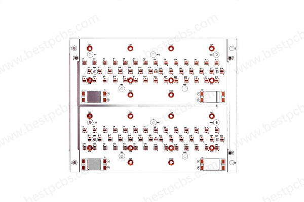
At EBest Circuit (Best Technology), we’ve been making LED PCBs for decades. We offer full support—from idea to finished board. Whether you need 1 piece for testing or 10,000 pieces for production, we’ve got you covered.
We manufacture:
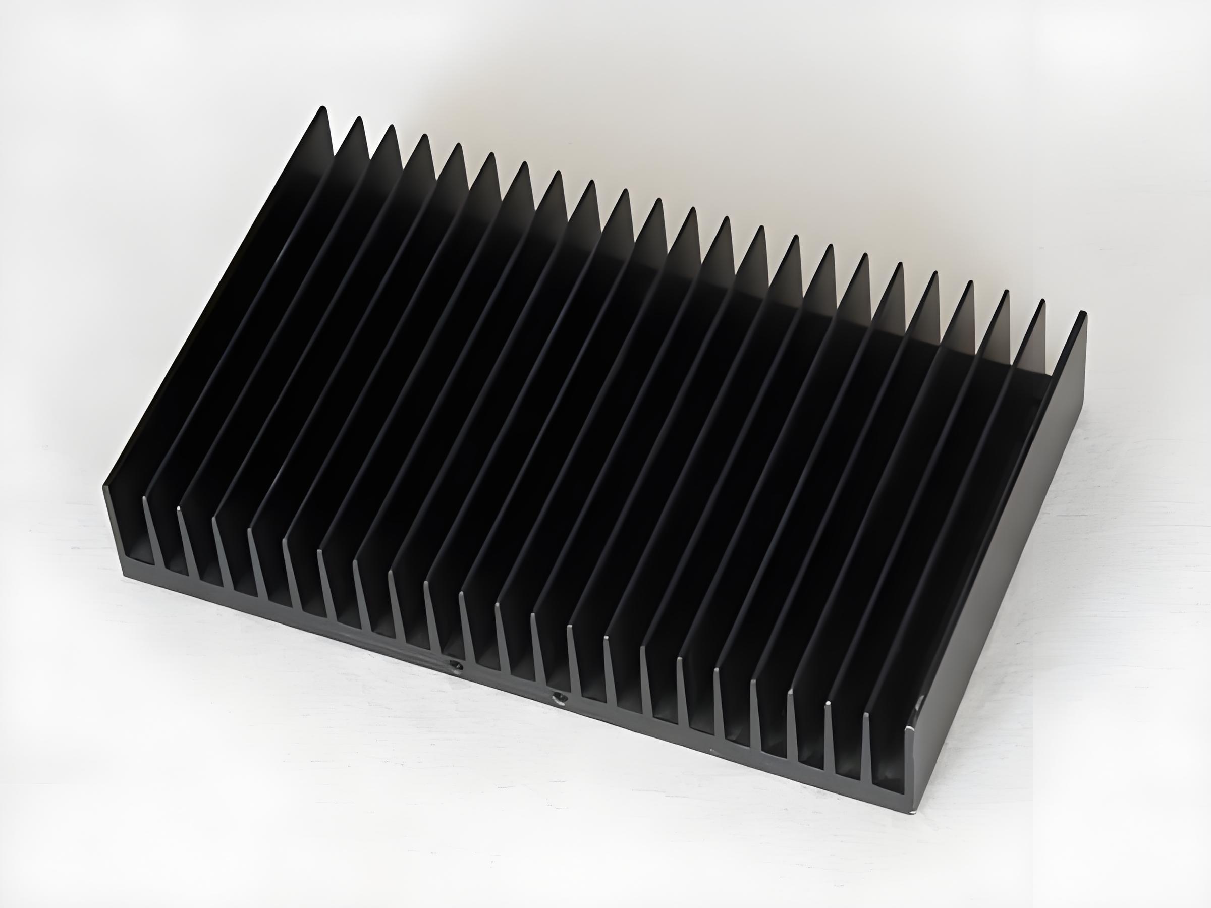
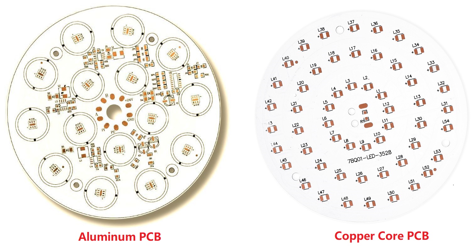
- Aluminum LED PCBs: Great for heat control
- FR4 LED PCBs: Good for low-power applications
- Ceramic LED PCBs: Perfect for small, hot environments
- Copper-based PCBs: Excellent for high current
We also provide:
- Free DFM checks (design for manufacturing)
- Quick samples (5–7 days turnaround)
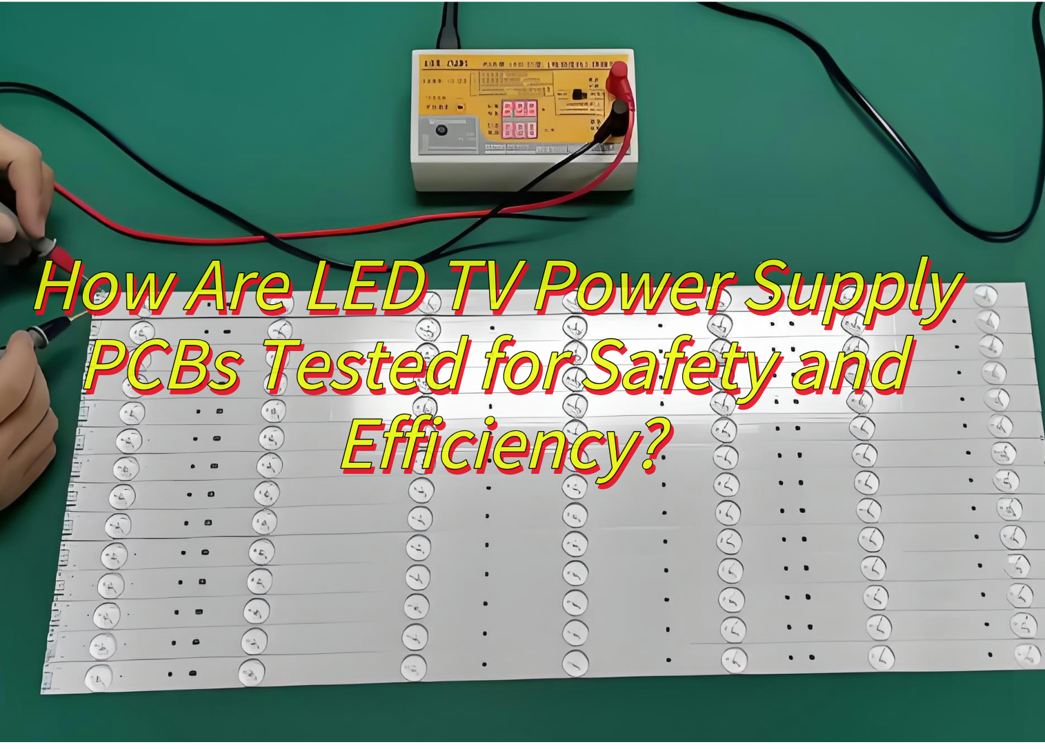
- Full testing (visual, electrical, thermal)
- Component sourcing and assembly
Our team understands both electronics and lighting design, so your custom LED PCB will meet your real-world needs.
Our LED PCB Capabilities
| Item | Capabilities |
| Layer Count | 1 – 10 Layers |
| Max Board Dimension | 24*64″(610*1625mm) |
| Min Board Thickness | 0.6mm |
| Max Board Thickness | 4.0mm |
| Conductor Thickness | 0.5oz – 10oz |
| Min Line Width/Line Space | 4/4mil (0.10/0.10mm) |
| Min Hole Diameter | 10mil (0.25mm) |
| Min Punch Hole Dia | 0.12″ (3.0mm) |
| Min Hole Spacing | 16mil (0.4mm) |
| Min PAD Ring(Single) | 3mil (0.075mm) |
| PTH Wall Thickness | Normal: 0.59mil (15um); HDI: 0.48mil (12um) |
| Min Solder PAD Dia | 14mil (0.35mm) |
| Min Soldermask Bridge | 8mil (0.20mm) |
| Min BAG PAD Margin | 5mil (0.125mm) |
| PTH/NPTH Dia Tolerance | PTH: ±3 mil (0.075mm); NPTH: ±2mil (0.05mm) |
| Hole Position Deviation | ±3mil (0.075mm) |
| Outline Tolerance | CNC: ±6 mil (0.15mm); Die Punch: ±6 mil (0.1mm) |
| Max Aspect Ratio | 10:01 |
| Surface Treatment | ENIG, ENEPIG, HAL, HASL(LF), OSP, Tin Imm |
Popular Applications of Custom LED PCBs
- Street Lighting
- Automotive Interiors and Headlights
- Backlighting for Displays
- Architectural and Accent Lighting
- Medical Imaging Devices
- Consumer Electronics
- Agricultural Grow Lights
Different environments need different board types. For example, a grow light needs stable, long-term brightness, while a car brake light needs to handle vibration and heat.
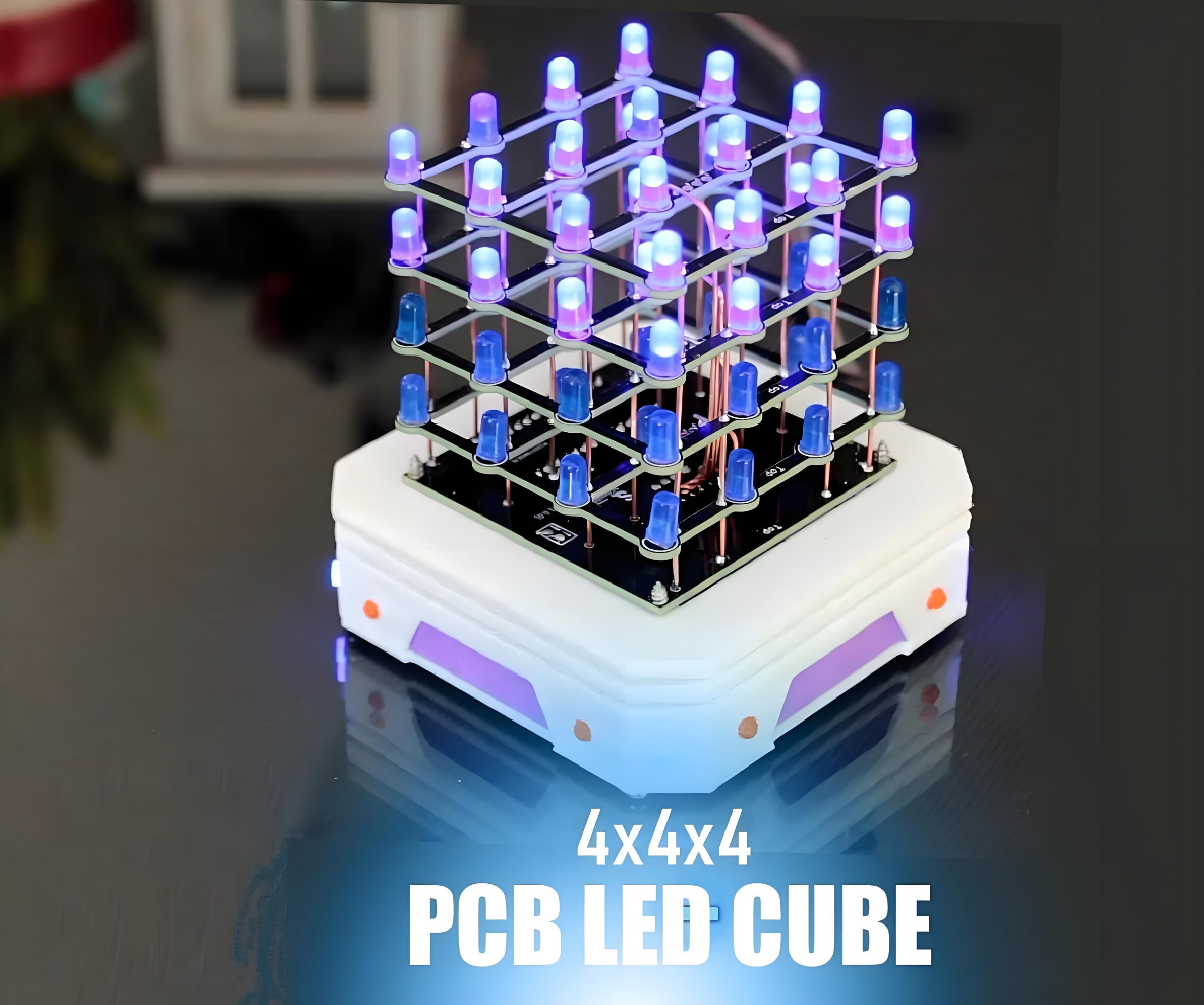
How to Design a DIY LED PCB Board?
Designing your own LED PCB can be a fun and educational project. Here’s how to get started:
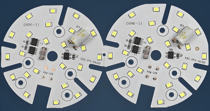
1. Pick your LED type: Decide how bright you want the light to be. Choose between small SMD LEDs or larger high-power ones.
2. Use design software: Free tools like EasyEDA or KiCad help you draw your circuit layout.
3. Decide on materials: If your LEDs will get hot, choose aluminum or copper as the base (though ceramic substrate has excellent thermal dissipation, but it is very expensive compared with aluminum or copper).
4. Draw your layout: Make sure LED placement is even. Place current paths (traces) wide enough to handle the power.
5. Add resistors: These control how much current goes through each LED.
6. Test your layout: Before making the board, simulate the circuit using the design software.
7. Order a prototype: Send your design to a PCB maker for a test run.
Tip: Always check the polarity of your LEDs before soldering—they only work one way!
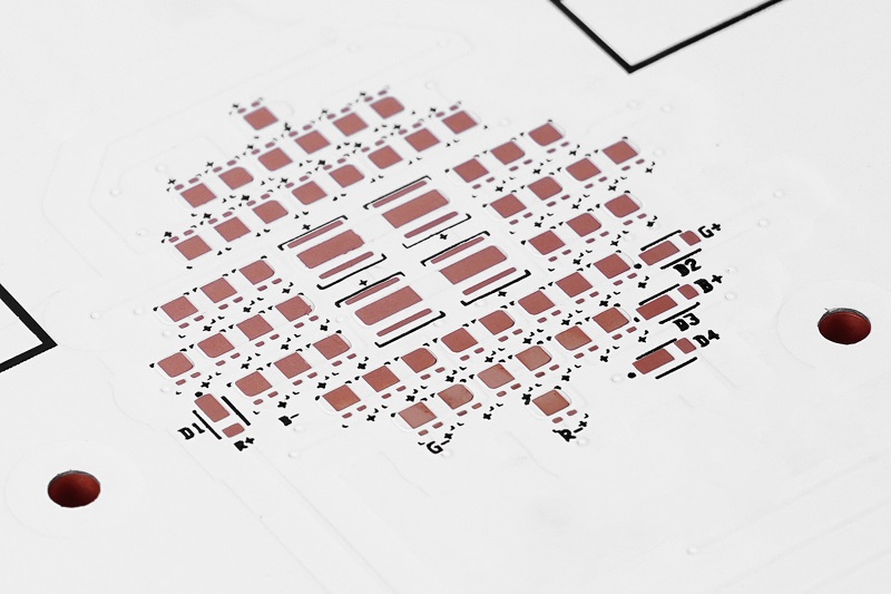
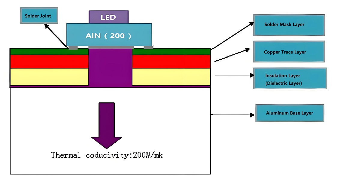
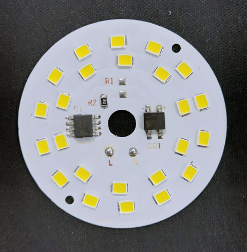
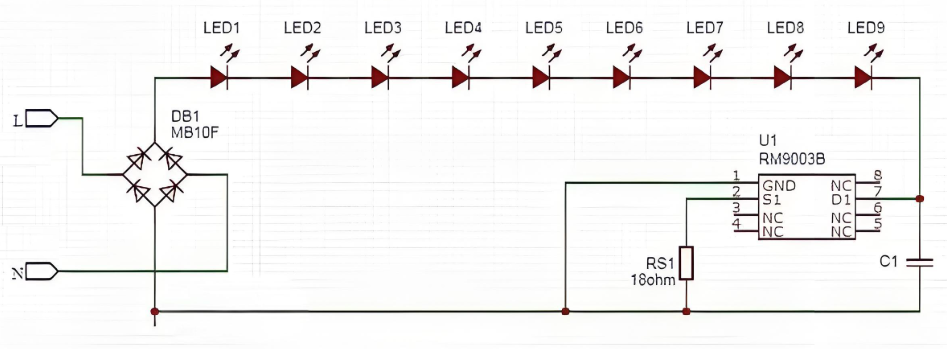
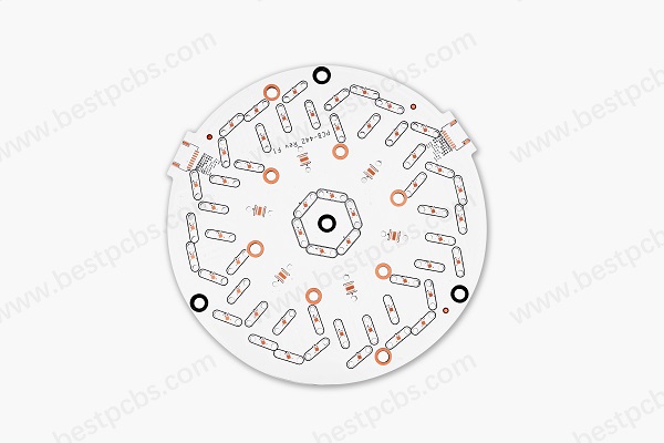
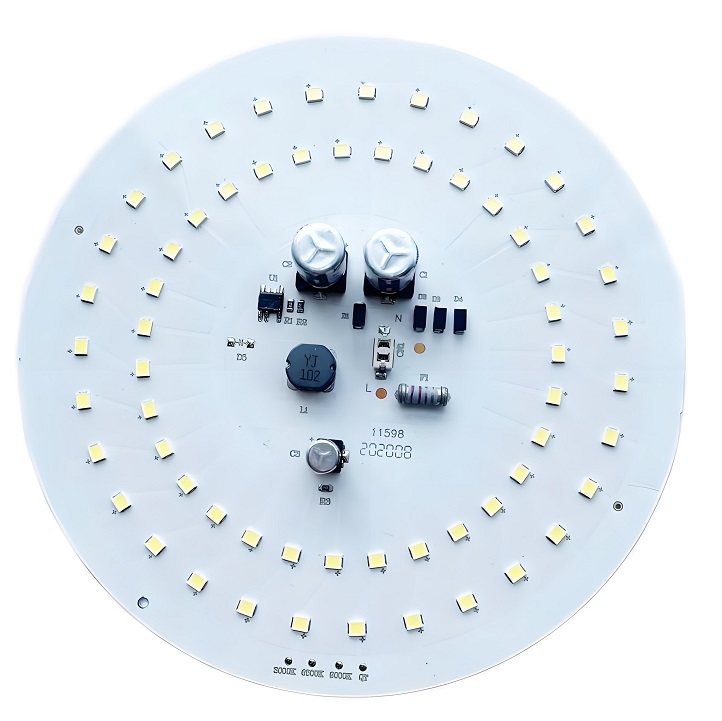
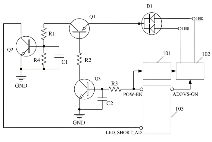
What’s Inside an LED Circuit Board Diagram?
An LED circuit diagram shows how the board works. It’s like a map for your board.
You’ll see:
- LEDs (usually marked with a triangle and line)
- Power input (VCC) and ground (GND)
- Resistors (to control current)
- Drivers or ICs (for smart control, if used)
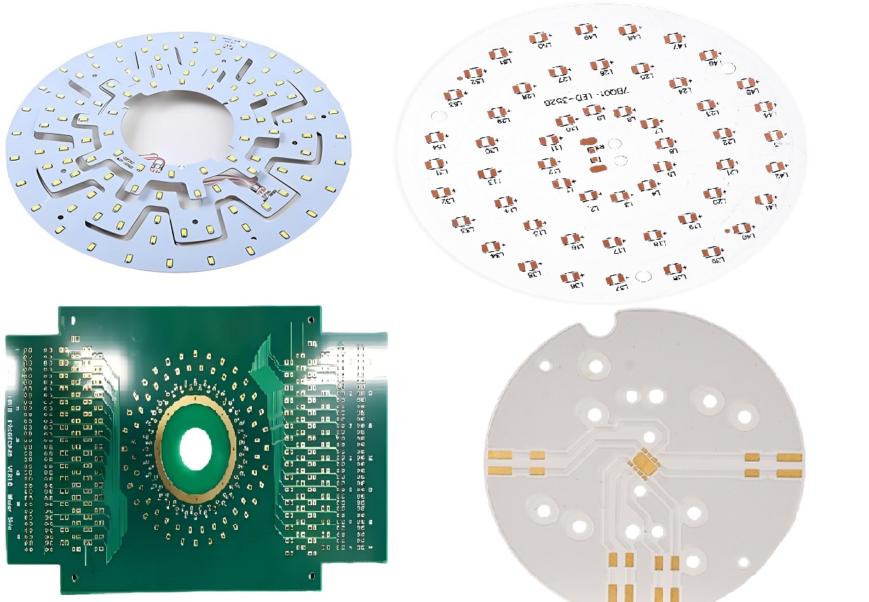
Here is a typical led circuit board diagram example:
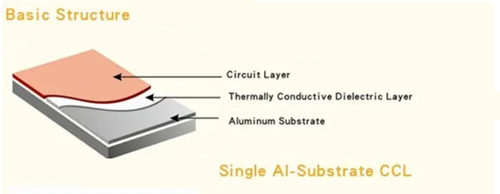
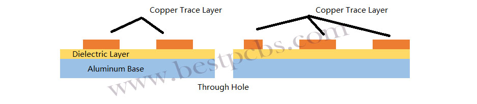
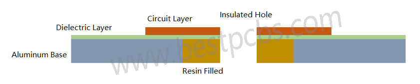
How to Choose the Right Base Material for Your LED PCB?
Choose the right material can help you save much time and money to revise or update the design. Nowadays, there are 5 types of base materials will be used in LED PCB design, each has unique properties and applications.
- Aluminum: Best for cooling and cost-effective. Used in most LED lights.
- FR4 (fiberglass): Cheap and easy to use. Works well for low-power lights.
- Ceramic (AlN or BeO): Great at handling heat. Used in medical or high-precision tools. It always used in high-end applications, like aerospace or military.
- Copper: Good conductor. Useful when you need a lot of power in a small space. But it has heavier weight among all materials.
- Polyimide: Flexible material, always used in flexible devices.
Tip: If your LED gets warm to the touch, go with aluminum or copper. If it stays cool, FR4 is usually fine.
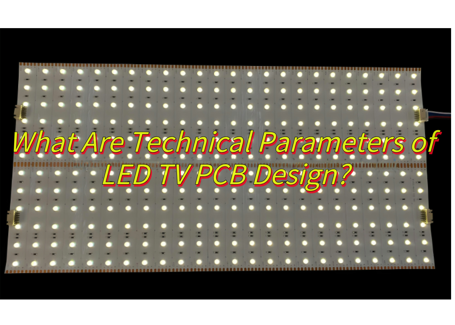
Key Considerations for LED PCB Strip Design
1. Current and voltage rating:
LED strips typically operate at standard voltages like 12V or 24V DC. Choosing the right voltage ensures consistent brightness and prevents overheating. For instance, a 24V strip loses less power over long runs compared to a 12V one—voltage drop is approximately 4–6% lower over a 5-meter run.
2. Copper thickness:
Standard copper thickness is 1oz, which is suitable for low-power strips. For high-current applications like industrial lighting, go for 2oz or more.
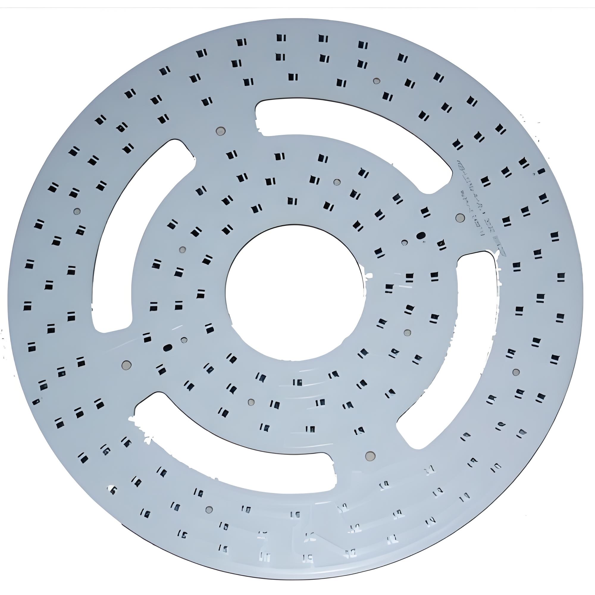
3. LED layout and spacing:
Spacing affects light uniformity and heat distribution. For example:
- 60 LEDs/m offers a soft glow suitable for accent lighting.
- 120 LEDs/m or higher gives a brighter, more uniform output, ideal for task lighting.
4. Solder mask color:
White and black solder mask are popular in led lighting design. White solder masks are preferred for LED strips because they reflect up to 80–90% of visible light, improving luminous efficiency. Black masks, on the other hand, absorb more heat and can reduce light output by up to 20% in reflective applications.
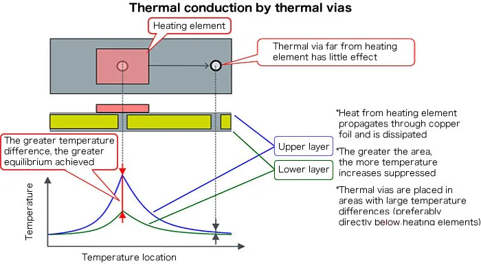
5. Thermal vias:
If you’re using a multi-layer PCB, thermal vias help transfer heat from the surface layer to the internal layers or to the aluminum base.
Whether you’re working on decorative lighting or industrial-grade illumination, these choices make a visible difference.
Common Mistakes to Avoid in LED PCB Board Replacement
Replacing an LED PCB board may seem simple, but several mistakes can lead to costly repairs or system failure. Here are a few things to watch out for:
1. Not matching the voltage and current ratings:
2. Poor heat management:
3. Wrong LED type or color temperature:
4. Using the wrong connectors or soldering techniques:
5. Skipping testing after installation:
EBest Circuit (Best Technology) offers replacement services and supports compatibility checks to avoid costly errors.
How to Get a Quote for a Custom LED PCB?
Getting a quote for a custom LED PCB is simple if you prepare the all information. Most of manufacturers are happy if you can provide following files in the quote phase.
1. Gerber files and BOM
2. Detailed Specifications:
- PCB size and shape
- Number of layers
- Copper thickness
- Base material (e.g., aluminum, FR4)
- Solder mask color
- Surface finish (ENIG, HASL, etc.)
3. LED details: mention the LED type, power rating, quantity, and placement.
4. Order quantity and lead time: higher volumes usually mean lower cost per unit. Also, let the supplier know if you need it urgently.
5. Special requirements: if you need waterproofing, specific connectors, or certifications (RoHS, UL, etc.) or IPC class III, include those details too.
If you have this information already, reach out EBest Circuit (Best Technology), and our sales team will review your files and send a best quotation within 12 hours.