Looking for PCB manufacturer in Argentina? This blog covers list and selection guide, evaluation methods of production capacity and lead time for PCB manufacturer in Argentina.
When searching for reliable PCB manufacturers in Argentina, understanding the landscape of top players is crucial to ensure informed decision-making. The PCB manufacturers in Argentina represent the most trustworthy options for meeting diverse PCB needs, from prototyping to large-scale production, and from standard rigid boards to specialized RF or HDI boards.
This guide highlights the key PCB manufacturer in Argentina options, breaking down their core strengths, production capabilities, and service offerings to help make informed decisions. Whether prioritizing fast turnaround times, strict quality control, competitive pricing, or specialized manufacturing processes, the top 10 PCB manufacturers in Argentina cover a range of expertise to align with different project requirements. By exploring the details of each manufacturer and the essential factors for evaluation, one can efficiently identify the right PCB manufacturer in Argentina to partner with, ensuring projects are delivered on time, within budget, and to the highest quality standards.
Are You Facing These Problems?
Inconsistent quality in PCB prototyping that leads to repeated design iterations and project delays.
Long lead times for PCB manufacturing that disrupt production schedules and market launch timelines.
Limited availability of specialized PCB design support for complex boards like HDI or RF boards.
Unclear pricing structures for PCB manufacturing that result in unexpected costs.
Lack of transparency in production processes, making it hard to track order progress.
Difficulty finding PCB manufacturers that accept low-volume orders (small MOQ) for custom projects.
End-to-End Support from Requirement to Delivery
We understand the challenges you face in sourcing reliable PCB manufacturer in Argentina, and we’ve developed comprehensive solutions to address each pain point head-on. For inconsistent prototyping quality, we implement rigorous pre-production testing and use high-grade materials to ensure every prototype meets your design specifications on the first try. To solve long lead times, we’ve optimized our production workflow and maintain a flexible production line that supports both standard and urgent orders, including 24-hour rapid prototyping. Our team of experienced engineers provides dedicated PCB design support for complex board types, offering technical guidance from concept to finalization. We maintain transparent pricing with detailed quotes that outline all costs upfront, eliminating unexpected expenses. Throughout the production process, you’ll have access to a real-time order tracking system, keeping you informed of every milestone. Additionally, we offer low MOQ options starting from 1 unit, making us an ideal partner for custom projects, small-batch productions, and large-scale orders alike. With our end-to-end support, you can focus on your core projects while we handle all aspects of PCB manufacturing with reliability and professionalism.
Why Choose EBest Circuit (Best Technology) for PCB Manufacturer?
Reasons Why Choose EBest Circuit (Best Technology) for PCB Manufacturer:
Uncompromising Quality: 100% automated optical inspection (AOI) for every batch, ensuring a defect rate below 0.01%, guaranteeing your products perform flawlessly in critical applications
Global Authority Certifications: Fully certified with ISO9001:2015, ISO13485:2016, REACH, RoHS, and IATF16949, meet strict industry standards for medical, automotive, and electronics sectors, no compliance risks.
Unbeatable Cost Efficiency: Optimized production processes + bulk material sourcing bring you 15-20% more competitive pricing than other PCB Manufacturer in Argentina, save costs without sacrificing quality.
Lightning-Fast Turnaround: Get standard orders delivered in 3-7 business days; 24-hour rapid prototyping for urgent requests, keep your projects on track and launch ahead of competitors.
19 Years of Proven Expertise: Nearly two decades in PCB manufacturing, we’ve mastered complex projects and solved countless technical challenges, your reliable partner for even the trickiest requirements.
All-In-One Turnkey Service: From PCB design consultation, prototyping to mass production and post-delivery support, one contact, full-process coverage, save you time and effort in coordination.
Ultra-Low MOQ Flexibility: Start orders from just 1 unit—perfect for prototypes, custom projects, and small-batch runs, no more wasting costs on unnecessary large orders.
Full Range of Customizable Products: Specialize in rigid, flexible, rigid-flex, metal core, ceramic, RF, HDI, and thick copper boards, fulfill any PCB demand for diverse industry scenarios.
Welcome to contact us if you have any request for PCB or PCBA service via this email: sales@bestpcbs.com.
Top 10 PCB Manufacturer in Argentina
Company Name
Main Business
Core Advantages
Process Capabilities
Lead Time
EBest Circuit (Best Technology) Co.,Ltd
PCB design, rigid/flexible/HDI/RF/metal core board prototyping & mass production
19-year experience, 24-hour rapid prototyping, 1-unit MOQ, global certifications
6-32 layer boards, 3mil/3mil line/space, 0.1mm via diameter, AOI/X-ray inspection
24h for prototypes, 3-7 days for standard orders
Argenprint S.A.
Multilayer PCB manufacturing for telecom/automotive/consumer electronics
20-year local expertise, ISO-certified, high reliability
1. Product Requirement Verification: Confirm manufacturer’s capability to produce rigid boards (2-20 layers, thickness 0.2-3.0mm), flexible boards (flexural life ≥100,000 cycles), HDI boards (line width/spacing ≤75μm), and RF boards (dielectric constant 3.5±0.1), ensuring coverage of project-required PCB characteristics.
2. Qualification Certification Check: Validate effectiveness of ISO9001 (Quality Management System), ISO13485 (Medical Devices, valid through December 2025), IATF16949 (Automotive Industry), and RoHS (Environmental) certifications to avoid compliance risks.
3. Delivery Time Alignment: Confirm standard lead time of 7-10 days and urgent order lead time of 3-5 days, matching project timelines (e.g., medical project requiring 8-day delivery).
4. Order Scale Adaptation: Evaluate MOQ of 100 rigid boards, 50 flexible boards, and 30 HDI boards, supporting small-batch customization (e.g., consumer electronics project with 200-piece batch demand).
5. Product Quality Verification: Require sample test data including impedance control accuracy ±5%, hole copper thickness ≥25μm, surface treatment uniformity ≤10%, or historical case yield ≥98%.
6. Price Transparency Comparison: Cross-check rigid board unit price with explicit breakdown of additional fees (e.g., testing/packaging) to ensure price-quality alignment.
7. Technical Support Evaluation: Confirm 24/7 online support, design optimization recommendations (e.g., 20% cost reduction via layer reduction), problem response time ≤2 hours, and complex project design assistance.
8. Market Reputation Review: Reference customer evaluation data including 95% satisfaction rate, 90% on-time delivery rate, 4.8/5 communication efficiency score, and case studies from medical/automotive industry leaders.
9. Production Transparency Requirement: Demand real-time production progress updates every 2 hours, visual monitoring of critical nodes (e.g., drilling/plating), and support for order status tracking.
10. After-Sales Service Consideration: Specify 7-day no-reason return/exchange, defect handling ≤3 days, return/exchange rate ≤1%, and detailed after-sales process with responsibility standards.
Core Pain Points of PCB Manufacturers in Argentina
Difficulty sourcing high-quality raw materials locally, leading to reliance on imports and potential supply chain delays.
High operational costs, including labor and production equipment maintenance, which can impact pricing competitiveness.
Limited access to advanced production technology for specialized PCB types, restricting the ability to cater to niche market needs.
Fluctuations in local regulations and import/export policies, creating uncertainty in production planning and supply chain management.
Shortage of skilled labor in specialized areas such as PCB design and high-precision manufacturing.
Challenges in meeting tight lead times for urgent orders due to limited production capacity during peak periods.
Pressure to comply with evolving environmental standards, requiring investment in eco-friendly materials and processes.
Intense competition from international PCB manufacturers offering lower pricing, making it hard to retain local customers.
How to Evaluate the Production Capacity of a PCB Manufacturer in Argentina?
Evaluation Guide to Production Capacity of PCB Manufacturers in Argentina:
Check monthly production volume: Assess if the manufacturer can handle your current and future order sizes
Inspect production facilities: Visit in-person or virtually to check if equipment is modern and well-maintained
Confirm production line capabilities: Ask about the number and specialization of lines to avoid bottlenecks for your specific PCB type
Review production history: Check their experience with similar projects and track record of fulfilling order quantities
Evaluate raw material management: Inquire about inventory systems to ensure a stable supply chain and avoid delays
Verify quality control at scale: Check their QC processes and testing equipment to ensure consistent quality during mass production
Assess production scalability: Ask if they can adjust output based on your changing needs, including lead times for increased orders
Check technical team strength: Inquire about the number of skilled workers and engineers to ensure sufficient human resources
Review third-party certifications: Check audits or certifications related to production capacity and quality management
Price Transparency Comparison: Cross-check rigid board unit price with explicit breakdown of additional fees (e.g., testing/packaging) to ensure price-quality alignment.
Technical Support Evaluation: Confirm 24/7 online support, design optimization recommendations (e.g., 20% cost reduction via layer reduction), problem response time ≤2 hours, and complex project design assistance.
Market Reputation Review: Reference customer evaluation data including 95% satisfaction rate, 90% on-time delivery rate, 4.8/5 communication efficiency score, and case studies from medical/automotive industry leaders.
How to Evaluate the Lead Time of a PCB Manufacturer in Argentina?
Evaluation Guide to Lead Time of PCB Manufacturer in Argentina:
Request a detailed breakdown of lead times for different order types (prototyping, small-batch, mass production) to ensure clarity on delivery timelines.
Ask for customer references to verify the manufacturer’s track record of meeting the promised lead times.
Inquire about the manufacturer’s production scheduling system to understand how they prioritize orders and handle urgent requests.
Check if the manufacturer has backup production capacity or partnerships to handle unexpected delays (e.g., equipment breakdowns, supply chain issues).
Inquire about the lead time for raw material procurement, as this is a key factor in overall order delivery.
Ask about the manufacturer’s order tracking system to ensure you can monitor progress and receive timely updates on any potential delays.
Discuss the manufacturer’s policy on late deliveries, including compensation or mitigation measures, to protect your project timeline.
Inquire about their ability to offer expedited services and the associated costs, in case you need to shorten the lead time.
Review the manufacturer’s historical data on on-time delivery rates, if available, to assess their reliability.
Production Transparency Requirement: Demand real-time production progress updates every 2 hours, visual monitoring of critical nodes (e.g., drilling/plating), and support for order status tracking.
After-Sales Service Consideration: Specify 7-day no-reason return/exchange, defect handling ≤3 days, return/exchange rate ≤1%, and detailed after-sales process with responsibility standards.
Frequently Asked Questions About PCB Manufacturing in Argentina
Q1. What PCB manufacturing capabilities are available in Argentina? A1. Most local manufacturers offer standard FR-4 boards, double-sided and 4-layer PCBs, basic HDI, and small-batch prototypes. Advanced stack-ups, RF materials, and large-volume orders are typically outsourced to Asia due to cost and equipment constraints.
Q2. How long does PCB production usually take in Argentina? A2. Standard lead time ranges from 7–15 working days for simple boards. Complex multilayers or HDI structures often extend to 20–30 days because of limited local capacity and material availability.
Q3. Are PCB prices in Argentina higher than in China or Southeast Asia? A3. Yes. Local pricing is generally 20–40% higher due to smaller production scale, imported materials, and higher operational costs. Many companies prototype locally but mass-produce overseas.
Q4. Can Argentine PCB factories handle HDI, microvia, or RF PCB? A4. Only a few can manage entry-level HDI and controlled impedance. RF boards using Rogers or Taconic are usually imported because specialty laminates are not always stocked locally.
Q5. What certifications do Argentina PCB manufacturers usually have? A5. Most local providers meet ISO 9001. Specialized automotive or medical certifications (IATF 16949, ISO 13485) are less common and often require outsourcing to certified Asian manufacturers
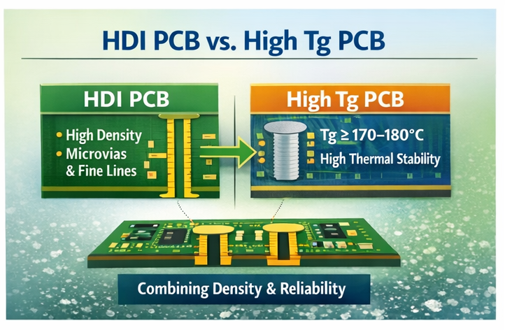
Why do HDI & high TG PCB solutions matter so much for high-reliability electronics? Because failures rarely come from a single “big” mistake. They often start from small issues: marginal solder joints, microcracks around vias, drift in impedance, or repeated thermal shock.
An HDI PCB helps by shortening trace length, controlling impedance, and reducing stubs. A high Tg PCB helps by raising the glass transition temperature, so the board structure stays stable under higher reflow and operating temperatures.
When you integrate both, you gain:
Better control of high-speed signals in dense layouts
Stronger resistance to repeated lead-free reflow cycles
Improved reliability in wide temperature ranges
Smaller, lighter boards that still carry complex circuits
For sectors like automotive ADAS, 5G equipment, and industry automation, this combination is often no longer “nice to have”. It becomes a base requirement.
What Are HDI & High Tg PCB Solutions?
HDI & High Tg PCB solutions refer to PCB designs that use high-density interconnection structures together with high-temperature glass transition materials. Rather than treating HDI PCB and high Tg PCB as separate topics, this concept views them as a design “toolbox” that works as a system.
A typical HDI & high Tg PCB stack-up may include:
High Tg FR4 or hybrid material core
One or more HDI buildup layers with microvias
Fine lines and spaces for dense routing
Controlled impedance structures for high-speed signals
Multiple lamination cycles using high Tg prepregs
These solutions focus on two goals at the same time: interconnection density and temperature endurance. The design approach covers layout rules, via strategy, material selection, and process limits from the start, not as late-stage fixes.
What Is an HDI PCB and Why Is It Used in Modern Electronics?
Sequential build-up (1+N+1, 2+N+2, 3+N+3, and so on)
Fine line/space (e.g., 75 µm/75 µm or better)
Via-in-pad for BGA breakout
Modern ICs such as high pin-count BGAs, fine-pitch QFNs, and SiP modules simply cannot be routed on old-style 1-via-per-pin layouts. HDI PCB structures shorten critical paths, reduce via stubs, and keep return paths tight.
Key advantages of hdi pcb in modern designs include:
Smaller board size with the same or higher function density
Better signal integrity for multi-gigabit links
Improved power distribution with dense stitching vias
Room for mechanical design freedom in slim devices
Because of this, HDI PCB technology is common in smartphones, tablets, communication modules, automotive radar, and compact industrial controllers.
What Is a High Tg PCB and How Does It Improve Reliability?
A high tg pcb uses laminate with a higher glass transition temperature than standard FR4. Tg is the point where the resin system changes from glassy to rubbery. Above this point, mechanical properties weaken quickly.
In a high Tg PCB, the Tg value might be 170–180°C or higher, instead of around 130–140°C for common materials. This increased Tg gives several benefits:
Better dimensional stability during lead-free reflow
Lower risk of pad lifting, delamination, or barrel cracks
Reduced mechanical stress during temperature cycling
Improved long-term reliability in high-temperature service
High Tg PCB materials also tend to have better thermal endurance over time, which helps in automotive under-hood zones, power supplies, motor drives, and LED lighting. They can handle more thermal stress without visible or hidden damage.
Differences Between HDI PCB and High Tg PCB
HDI and high Tg describe two different aspects of a PCB: one structural, one material. They often coexist, but they are not the same.
Aspect
HDI PCB
High Tg PCB
Main focus
Interconnect density and routing
Thermal and mechanical stability
Key features
Microvias, fine lines, via-in-pad
Tg ≥ 170–180°C, better thermal endurance
Typical driver
Fine-pitch BGAs, compact form factor
Lead-free reflow, high operating temperature
Impact on layout
Strong effect on routing and stack-up
Moderate; affects stack-up and DFM margin
Impact on reliability
Better signal and via performance
Lower risk of warpage and delamination
Cost drivers
Laser drilling, lamination cycles, yield
Material price, process window, lamination setup
An HDI PCB can use standard Tg material when the thermal profile is mild. A high Tg PCB can have no HDI features at all if density remains low. When the project pushes both limits, you combine them.
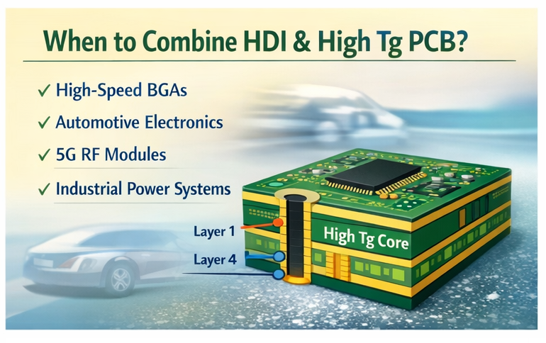
When Should HDI PCB and High Tg PCB Be Combined?
Combining HDI PCB and high Tg PCB makes sense when a design faces both density and thermal stress at the same time. Typical cases include:
High-speed compute boards with large BGAs and multiple reflow passes
Automotive radar or camera modules near engines or outdoor zones
5G RF front-ends in compact housings with limited airflow
Industrial motion control or power electronics running at elevated temperature
You should consider an HDI & high Tg PCB solution if:
The layout requires microvias or sequential lamination to escape key components
The assembly line uses lead-free profiles with high peak temperature
The product will see frequent on-off cycling or wide ambient temperature swings
Field reliability and long service life carry high business value
In these scenarios, HDI brings routing freedom and signal quality, while high Tg materials protect the board structure against thermal and mechanical stress.
Medical devices: Imaging equipment, patient monitoring, compact diagnostic tools
Consumer and wearable devices: Smartphones, tablets, smartwatches, AR/VR devices
All these products share common requirements: compact size, strict reliability targets, and long-term stability under shifting loads. HDI PCB structures handle fine-pitch and high-speed paths, while high Tg PCB materials carry the thermal and mechanical burden.
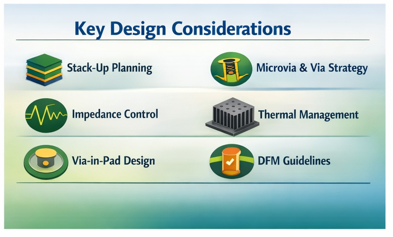
What Are the Key Design Considerations for HDI & High Tg PCB?
Designing HDI & high Tg PCB solutions is not just about choosing a material with higher Tg and shrinking traces. It needs careful coordination between layout, stack-up, and process limits. Key points include:
1. Stack-up planning early
Decide the HDI level (1+N+1, 2+N+2, etc.), copper thickness, and layer count early. Include high Tg material data, Dk/Df values, and lamination constraints in the first draft.
2. Microvia and buried via strategy
Keep microvia aspect ratios within the fabricator’s safe range. Use staggered rather than stacked microvias when reliability priority is high, unless the project can support enhanced filling processes.
3. Impedance control with high-speed pairs
High-density routing often pushes traces close together. Work with the fabricator to set precise trace width and spacing for each impedance class, considering the actual dielectric constant of the high Tg material.
4. Thermal management and copper balance
High Tg PCB materials support higher temperature, but heat still needs paths. Balance copper areas across the panel to reduce warpage. Provide solid ground planes, thermal vias, and clear heat paths.
5. Solder mask and via-in-pad design
When using via-in-pad on HDI pads, confirm filling and capping processes. Poorly filled vias can trap flux or reduce solder joint strength.
6. Design for manufacturability (DFM)
Follow the manufacturer’s design rules for minimum line/space, annular ring, drill size, and pad shapes. Good DFM work reduces scrap and supports stable quality.
What Manufacturing Challenges Exist in HDI & High Tg PCB?
Manufacturing HDI PCB involves several engineering challenges because the process pushes the limits of micro-fabrication, interlayer reliability, material control, and inspection accuracy. Each stage demands strict tolerance management to keep performance stable in high-density layouts.
Microvia and blind-via drilling accuracy is difficult because HDI requires via diameters
below 0.15 mm. Laser drilling must stay stable and precise to avoid rough walls, incomplete holes, or weak plating that may cause electrical issues in stacked via structures.
Layer-to-layer registration and lamination control demand micron-level alignment.
High-order HDI needs multiple lamination cycles, and any shift in imaging, resin flow, or pressure can create opens, shorts, or signal loss.
Fine-line etching becomes harder as line width and spacing drop to 3 mil or less. Thin
traces are sensitive to under-etching or over-etching, and thicker copper (4–10 oz) makes precise control even more challenging.
Plating and via filling must deliver uniform copper to keep interconnections stable.
Voids, trapped gas, or uneven filling weaken microvias and reduce long-term reliability, especially when the design needs high breakdown voltage.
How EBest Circuit (Best Technology) Supports HDI & High Tg PCB Solutions?
EBest Circuit (Best Technology) supports HDI & High Tg PCB Solutions from early design review through mass production and assembly. Our team focuses on turning demanding ideas into stable, repeatable products.
Engineering and DFM for HDI and high Tg
Our engineers review your stack-up, HDI level, and component layout at the start. We suggest suitable high Tg materials, via strategies, and impedance structures based on your performance and cost targets.
HDI PCB manufacturing capability
We support fine line and space routing, laser-drilled microvias, via-in-pad, and multi-step lamination. Typical HDI builds such as 1+N+1, 2+N+2, and higher structures can be handled with controlled registration and repeatable yields.
High Tg and advanced materials
We work with well-known high Tg PCB laminates and can also support hybrid builds for projects that need both RF and digital performance. Material selection focuses on Tg, Td, Dk/Df, and reliability under your real reflow profile.
PCBA assembly with process control
EBest Circuit (Best Technology) provides SMT and through-hole assembly for HDI and high Tg boards in both China and Vietnam. Lead-free profiles, X-ray for BGA, and AOI help keep quality stable for dense layouts.
Quality systems and traceability
Our factories follow ISO9001, ISO13485 for medical, IATF16949 for automotive, and AS9100D for aerospace. We also run MES systems to track each lot from material incoming through final shipment. This supports clear traceability and faster root-cause analysis if any issue appears.
For buyers who need a long-term partner for HDI & high Tg PCB solutions, this combination of engineering support, HDI process capability, and certified quality systems reduces risk and saves internal effort.
FAQs about HDI & High Tg PCB Solutions
1. Is HDI PCB always more expensive than a standard multilayer board?
HDI PCB usually costs more per panel due to laser drilling, extra lamination, and tighter controls. However, the total product cost can drop because the board is smaller, the BOM can be simplified, and performance improves.
2. When do I really need a high Tg PCB instead of normal FR4?
You should consider a high Tg PCB when your design uses lead-free solder, has more than one reflow cycle, or runs in high ambient temperatures. Automotive, power, and industrial products are common cases where high Tg material significantly improves reliability.
3. Can I use HDI without high Tg material for consumer products?
Yes. Many consumer devices use hdi pcb structures on mid-range Tg materials because their operating temperature is moderate and lifetime targets are shorter. The decision depends on your thermal profile and reliability goals.
4. Are stacked microvias less reliable than staggered ones?
Stacked microvias can be reliable when the process is well controlled, but they need stricter plating and filling quality. For very harsh environments, many designers still prefer staggered microvias for extra margin, unless dense routing forces stacking.
5. How early should I involve EBest Circuit (Best Technology) in an HDI & high Tg PCB project?
The best time is before you freeze the stack-up and routing strategy. Early DFM and material discussion help avoid later redesign, reduce risk, and shorten the path from prototype to stable mass production.
If you are planning a new design that needs smaller size, higher speed, and stronger thermal performance, HDI & High Tg PCB Solutions may be the right direction. You can share your Gerber files, stack-up ideas, or even just a concept, and EBest Circuit (Best Technology) will help you evaluate practical options, costs, and timelines for your next project.
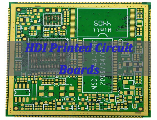
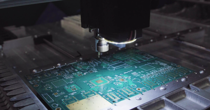
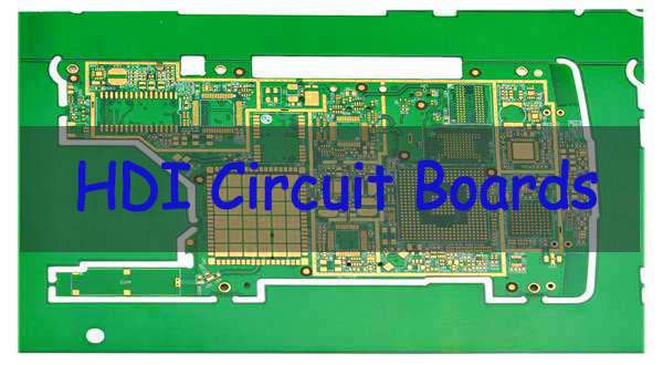
HDI printed circuit boards are advanced multilayer boards that utilize high-density interconnect technology to accommodate more components in a smaller area, enabling the miniaturization and enhanced performance of modern electronics. This comprehensive guide will explore the intricacies of HDI PCB technology, its manufacturing process, and the critical importance of choosing a partner with full turnkey capability for your project’s success.
Navigating the complex world of advanced PCB procurement can be fraught with challenges. Are you struggling to balance high performance with tight project constraints? Common pain points include:
Managing Sky-High Complexity: HDI designs with microvias and multiple lamination cycles introduce significant manufacturing and design validation hurdles.
Controlling Unpredictable Costs: Quotes that spiral due to unforeseen process steps, material waste, or yield issues with delicate HDI structures.
Suffering from Fragmented Supply Chains: Coordinating separately with design houses, board fabricators, and assembly shops leads to communication gaps, finger-pointing, and delayed timelines.
Ensuring Reliable Performance: Anxiety over signal integrity in dense layouts and the long-term reliability of microvias under thermal and mechanical stress.
Navigating Opaque Vendor Capabilities: Difficulty verifying if a supplier truly has the specialized equipment and expertise for your specific HDI level and technology needs.
The most effective path to mitigating these risks is partnering with a manufacturer that offers genuine full turnkey capability. This means:
Integrated Design Support: Expert HDI PCB design guidance from the start to prevent costly manufacturability issues.
Transparent Cost Engineering: Clear cost breakdowns and design-for-manufacturing (DFM) advice to optimize the HDI printed circuit boards price.
Seamless Process Ownership: A single point of accountability managing the entire flow from Gerber files to tested assemblies.
Advanced Process Validation: Rigorous testing protocols, including cross-sectioning and thermal cycling, for reliability assessment of microvias in HDI printed circuit boards.
Demonstrable Technical Expertise: Clear evidence of in-house advanced equipment and a proven track record with complex HDI builds.
At BEST Technology, we specialize in transforming these complex challenges into seamless solutions. As a professional HDI PCB manufacturer with robust full turnkey services, we own and manage the entire process—from design review and prototyping to sophisticated fabrication, precise assembly, and rigorous testing. Our expertise ensures your high-density interconnect projects are not only manufacturable but also optimized for performance, cost, and reliability. For your next project, pls feel free to contact our experts at sales@bestpcbs.com.
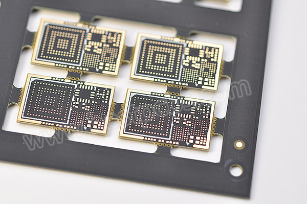
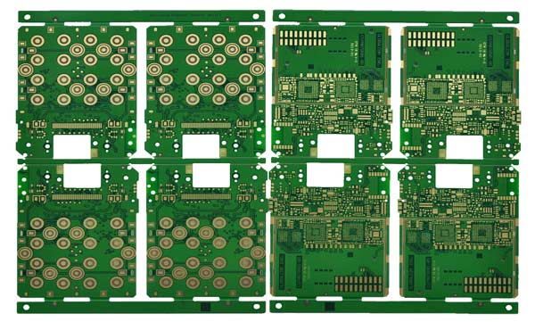
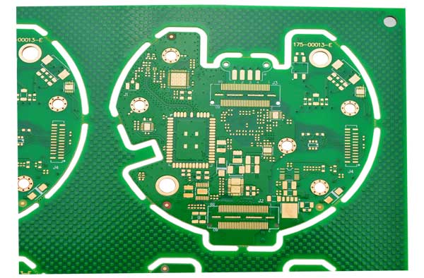
What are HDI Printed Circuit Boards?
HDI printed circuit boards are advanced PCBs designed for high wiring density and compact electronic systems. They rely on microvia technology, fine-line routing, and multilayer stackups to support complex interconnections within limited board space.
Key characteristics of HDI printed circuit boards include:
High wiring density Enables more signal routing and component placement in smaller board areas.
Microvia technology Uses laser-drilled blind and buried vias, typically ≤ 0.15 mm in diameter, to replace traditional mechanical through-holes.
Fine line width and spacing Supports ultra-fine traces and tight spacing for high-density component layouts.
Advanced multilayer stackups Incorporates sequential lamination and any-layer interconnect structures for greater design flexibility.
Improved signal integrity Shorter interconnect paths and optional low-Dk/Df materials help maintain performance in high-speed designs.
Specialized manufacturing processes Requires precision laser drilling, controlled lamination, and strict process control during the HDI PCB manufacturing process.
In summary, HDI printed circuit boards are not simply denser versions of standard PCBs. They represent a dedicated design and manufacturing approach that enables modern, high-performance electronic products with strict size and performance constraints.
What Makes HDI Circuit Boards Different From Standard Multilayer PCBs?
While both are multilayer structures, HDI PCBs are fundamentally different in their construction and capabilities. Standard multilayer PCBs use mechanical drilling for through-hole vias, which limits density. HDI circuit boards, however, are defined by their use of microvias (typically with a diameter of less than 150µm), which allow for direct interconnections between adjacent layers, unlocking new routing possibilities.
Feature
Standard Multilayer PCB
HDI PCB
Via Technology
Primarily through-hole vias
Microvias, blind/buried vias
Line Width/Space
Larger (e.g., ≥ 4 mil)
Finer (e.g., ≤ 3 mil)
Pad Density
Lower
Much Higher
Construction
Fewer lamination cycles
Multiple sequential laminations
Key Benefit
Cost-effective for simpler designs
Enables miniaturization & high-speed performance
The distinction lies in the high density interconnect approach, which provides superior electrical performance and design freedom, making it ideal for complex, space-constrained applications.
What Is the Structure of HDI Printed Circuit Boards?
The structure of HDI printed circuit boards is not defined by a single, fixed stackup or manufacturing flow. Instead, HDI construction is highly flexible and is determined primarily by via requirements, drilling methods, and interconnection density. The layer structure and production sequence are customized to meet specific routing and component layout demands.
At the core of HDI PCB structure is the combination of multiple via types, each serving a different interconnection purpose:
Laser-drilled blind vias These microvias connect an outer layer to one or more adjacent inner layers. They are a defining feature of HDI printed circuit boards and enable high routing density while minimizing signal path length.
Mechanically drilled buried vias Buried vias connect inner layers without reaching the outer surfaces. They support complex multilayer interconnections and help free surface area for fine-pitch components.
Mechanically drilled through holes Through holes extend from the top layer to the bottom layer and are typically used for power distribution, grounding, or components that require mechanical strength.
Because HDI printed circuit boards often rely on sequential lamination, the final structure may include multiple build-up layers, stacked or staggered microvias, and hybrid via combinations. As a result, each HDI design follows a drilling-driven structural logic, rather than a standardized process template.
In practice, the structure of HDI printed circuit boards is engineered around via architecture, layer interconnect strategy, and manufacturing feasibility, allowing designers to balance density, reliability, and performance in advanced electronic systems.
What Are the Blind Via Types in HDI Printed Circuit Boards?
In HDI printed circuit boards, blind vias are created primarily by laser drilling and are used to connect surface layers to inner layers without penetrating the entire board. Different blind via structures are selected based on layer count, routing density, and reliability requirements.
Common blind via types used in HDI printed circuit boards include:
Microvia hole Typically used in 1+N+1 HDI structures, microvias connect the outer layer to the adjacent inner layer. These vias are laser-drilled and are not copper-filled, making them suitable for simpler HDI designs with moderate density requirements.
Solid via hole (filled microvia) Also applied in 1+N+1 structures, solid vias are laser-drilled microvias that require copper filling. The filled structure provides a flat surface for component pads and supports higher reliability and finer pitch components.
Staggered via hole Used in second-order HDI, staggered vias consist of offset laser-drilled microvias on different layers. This structure reduces stress concentration and is commonly chosen for improved reliability in multilayer HDI designs.
Stacked via hole A key feature of high-density and any-layer HDI, stacked vias are vertically aligned laser-drilled microvias. These vias must be copper-filled to ensure mechanical strength and electrical continuity across multiple layers.
Skip via hole Skip vias are laser-drilled microvias that connect non-adjacent layers, such as from layer 1 directly to layer 3, bypassing layer 2. This structure increases routing flexibility while maintaining surface density.
Step via hole Step vias are co-located second-order laser vias that are not copper-filled. They are typically used in designs where surface planarity is less critical but routing density must still be increased.
How to distinguish blind via structures in HDI designs:
Whether the design is 1+N+1 This indicates the most basic HDI build-up structure, where laser-drilled blind vias connect the outer layers to the adjacent inner layers.
Whether the design is second-order HDI Second-order HDI involves connecting to deeper layers using two sequential microvias, typically requiring either staggered or stacked via structures.
Staggered vs. stacked vias The key distinction is whether the two microvias are vertically aligned.
Staggered vias are offset between layers.
Stacked vias are directly aligned on the same vertical axis.
Filled vs. non-filled vias
Designs using via-in-pad, requiring high surface planarity or higher long-term reliability, typically require copper-filled vias.
Vias that are not located in pads and are used in cost-sensitive designs may remain unfilled, depending on reliability requirements and manufacturing capability.
Each blind via type in HDI printed circuit boards serves a specific structural and electrical function. The selection depends on factors such as layer stackup, component pitch, signal integrity requirements, and manufacturing capability, making blind via design a critical part of HDI PCB engineering.
What Equipment Do HDI Printed Circuit Boards Factories Use for Microvias?
UV or CO₂ Laser Drilling Machines: For ablating precise, small-diameter microvias (as small as 50µm).
Advanced Direct Imaging (DI) Systems: To expose ultra-fine line traces and spaces with high accuracy.
Fully Automated Optical Inspection (AOI): To detect minute defects in traces, spaces, and via pads.
Electroless and Electrolytic Copper Plating Lines: For uniform copper deposition into high-aspect-ratio microvias.
Sequential Lamination Presses: To build the multilayer structure with precise layer-to-layer registration. This specialized toolset is non-negotiable for achieving the yields and quality required in the competitive HDI printed circuit board market.
How to Identify HDI Levels in HDI Printed Circuit Boards?
Identifying the HDI level of HDI printed circuit boards primarily depends on the via structure, rather than on trace etching or basic layer count. While routing processes for multilayer PCBs are largely similar to those used for single- or double-layer boards, the defining difference lies in how vias are formed and interconnected.
At a high level, PCB constructions can be classified into through-hole boards, first-order HDI, second-order HDI, and stacked HDI. Higher-order and any-layer HDI structures exist, but they are used far less frequently due to significantly higher cost and manufacturing complexity.
Through-Hole Boards (Non-HDI)
Through-hole boards use a single via type that runs from the top layer to the bottom layer. All interconnections—both outer and inner—are completed using mechanically drilled through holes that are subsequently copper plated.
The number of layers does not determine whether a board is HDI. A 2-layer PCB is typically a through-hole board, but many high-end products such as network switches or military electronics use 20-layer boards that are still entirely through-hole. Typical finished via diameters range from 0.2 mm to 0.3 mm, with smaller diameters increasing cost due to drill wear and slower drilling speeds.
First-Order HDI (1st-Order HDI)
A first-order HDI board is identified by the presence of one layer of laser-drilled microvias on each outer surface. These microvias usually have diameters around 0.1 mm and connect the outer layers to the adjacent inner layers.
Structurally, a common example is a 6-layer first-order HDI board, which can be viewed as a 4-layer through-hole core with one HDI build-up layer added to each side. The inner layers still rely on mechanical vias, while the outer layers use laser microvias.
Laser drilling only penetrates dielectric material and does not cut through copper, allowing precise via formation without damaging internal circuitry.
Second-Order HDI (2nd-Order HDI)
A second-order HDI board contains two layers of laser-drilled microvias on each side of the core. In practical applications, second-order HDI structures are most commonly found in 8-layer or higher designs, rather than in 6-layer boards.
There are two main second-order configurations:
Staggered vias The two layers of laser microvias are offset from each other. This approach is used because unfilled microvias cannot reliably support another laser via drilled directly on top. Staggered structures reduce process risk and are more cost-effective.
Stacked vias In stacked structures, the laser microvias are vertically aligned. To make this reliable, the lower microvia must be copper-filled before drilling the upper microvia. This process is more complex and significantly more expensive but enables tighter routing density.
In terms of structure:
A 6-layer second-order HDI board can be viewed as a 4-layer first-order board with an additional HDI build-up.
An 8-layer second-order HDI board is effectively a 6-layer first-order board with another build-up layer added.
Any-Layer HDI
Any-layer HDI represents the highest level of HDI technology. Every layer is interconnected using laser-drilled microvias, and any layer can connect directly to any other layer.
This structure offers maximum routing freedom and density, making layout significantly easier for engineers. However, the cost is extremely high—often more than ten times that of a standard through-hole board—so any-layer HDI is reserved for only the most compact and performance-critical designs.
In practice, HDI levels in HDI printed circuit boards are identified by answering three key questions:
Are laser-drilled microvias present? If not, the board is a through-hole design.
How many layers of microvias are used? One layer indicates first-order HDI; two layers indicate second-order HDI.
Are the microvias staggered or stacked? Staggered vias suggest cost-optimized second-order HDI, while stacked vias indicate higher-density, higher-cost designs.
By examining via type, drilling method, and build-up layer count, the HDI level of a printed circuit board can be accurately determined, independent of total layer count alone.
How Does HDI Technology in PCB Improve Signal Integrity?
HDI technology in PCB is a cornerstone for high-speed digital and RF applications because it inherently enhances signal integrity (SI).
Shorter Interconnect Paths: Microvias enable more direct routing, reducing signal path length and propagation delay.
Reduced Parasitics: Smaller via stubs and pads lower parasitic inductance (L) and capacitance (C), minimizing unwanted signal reflection and attenuation.
Better Impedance Control: Finer lines and consistent dielectric layers allow for more precise control over characteristic impedance.
Improved Power Integrity: Dense via-in-pad technology provides low-inductance paths for power delivery networks (PDNs), reducing switching noise.
Enhanced EMI/EMC Performance: Tighter component placement and optimized grounding via microvias help contain electromagnetic interference. These SI benefits make HDI printed circuit boards essential for 5G, high-performance computing, and advanced automotive electronics.
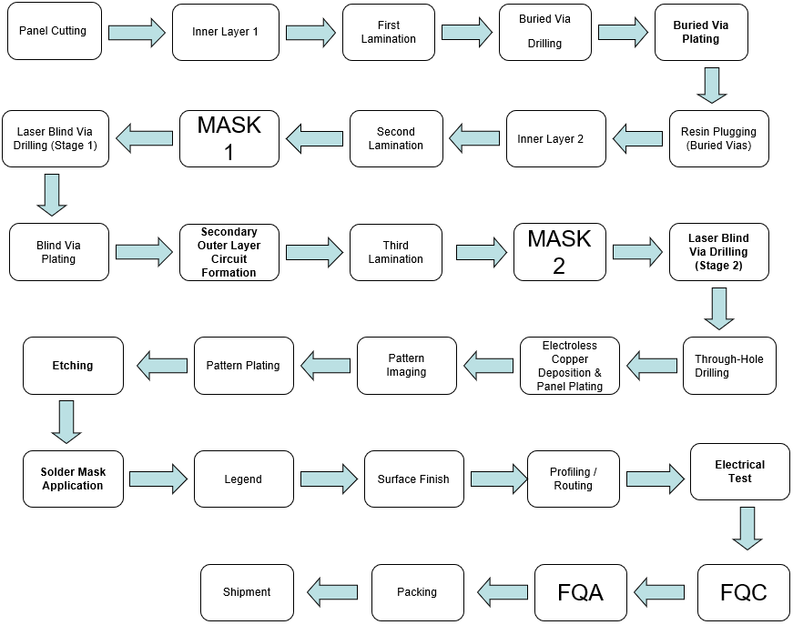
HDI PCB Manufacturing Process Explained Step by Step
In HDI production, the “step-by-step” flow changes with the stackup and via strategy.
Example 1: 1+4+1 (B) Process Flow
(Two lamination cycles, with inner mechanical drilling and plating performed before the second lamination, then laser microvias after the second lamination.)
Panel Cutting
Inner Layer Imaging & Etching
1st Lamination (First Press)
L2–L5 Mechanical Drilling
L2–L5 Copper Plating
L2–L5 Inner/Outer Layer Circuit Formation (for the sub-structure)
2nd Lamination (Second Press)
Laser Drilling (Microvias)
Mechanical Drilling (Through Holes / Tooling Holes as required)
Copper Plating (Via Metallization)
Outer Layer Imaging & Etching
Solder Mask Application
ENIG (Electroless Nickel Immersion Gold)
Legend / Silkscreen Printing
Profiling / Routing (Final Outline)
Electrical Test (E-test)
Final Inspection
OQC (Outgoing Quality Control)
Packing
Warehouse Receiving (Stock-in)
Example 2: 1+4+1 (A) Process Flow
(Single lamination cycle, then laser drilling and standard downstream flow.)
Panel Cutting
Inner Layer Imaging & Etching
Lamination (Pressing)
Laser Drilling (Microvias)
Mechanical Drilling (Through Holes / Tooling Holes as required)
Copper Plating (Via Metallization)
Outer Layer Imaging & Etching
Solder Mask Application
ENIG (Electroless Nickel Immersion Gold)
Legend / Silkscreen Printing
Profiling / Routing (Final Outline)
Electrical Test (E-test)
Final Inspection
OQC (Outgoing Quality Control)
Packing
Warehouse Receiving (Stock-in)
The practical difference between 1+4+1 (A) and 1+4+1 (B) is whether the build requires a staged sequence with an early drill-and-plate step before the second lamination. That staged approach adds process control points and complexity, which often affects lead time and cost.
Example 3: 1+1+8+1+1 Process Flow
Using a 12-layer, double-lamination first-order HDI structure (1+1+8+1+1) as an example, the following briefly outlines the standard manufacturing process commonly used in the industry.
What Applications Use HDI Circuit Boards Most Frequently?
HDI circuit boards are most widely used in applications that demand high signal density, compact form factors, and reliable high-speed performance. As electronic systems continue to evolve toward higher integration and smaller footprints, HDI technology has become a foundational solution across several major industries.
Consumer Electronics and Smartphones
Smartphones remain the largest application segment for HDI circuit boards, accounting for more than half of total HDI demand. Modern smartphone mainboards rely heavily on HDI structures to support high pin-count processors, dense memory interfaces, and multi-antenna RF layouts within extremely limited space.
HDI enables fine line routing, multi-layer interconnects, and compact board stacking, making it essential for slim device profiles and advanced functionality. Wearable electronics further extend this demand, using HDI and embedded via technologies to significantly reduce PCB area.
PC, Consumer Computing, and High-Performance Devices
PCs, tablets, and other consumer computing products represent a rapidly expanding HDI application area. As processors become more powerful and interfaces move toward higher speeds, HDI circuit boards are increasingly adopted to meet routing density and signal integrity requirements.
This segment has grown to roughly one-third of overall HDI demand, driven by compact laptops, high-performance computing modules, and emerging AI-enabled consumer devices.
Automotive Electronics and ADAS Systems
Automotive electronics, particularly ADAS and intelligent vehicle platforms, are a fast-growing HDI application. Vehicle systems require HDI circuit boards to support synchronized multi-sensor signal processing, high-speed data transmission, and stable operation under thermal stress and vibration.
HDI technology enables reliable high-density interconnects for camera modules, radar systems, and in-vehicle infotainment, making it a critical component in the transition toward autonomous and intelligent vehicles.
Communication Infrastructure and 5G Equipment
HDI circuit boards are widely used in 5G base stations and communication equipment, where high-frequency, low-loss signal transmission is essential. These systems require fine-line HDI layouts to support large antenna arrays, RF front-end integration, and high-speed signal processing.
The increasing complexity of 5G infrastructure continues to push higher layer counts and tighter precision requirements, accelerating HDI adoption in telecom applications.
Medical Electronics and Healthcare Devices
Medical electronics represent a smaller but high-value HDI segment. Advanced imaging systems, implantable medical devices, and portable diagnostic equipment rely on HDI circuit boards to achieve miniaturization, high reliability, and precise signal acquisition.
HDI flexible and rigid-flex structures are particularly important in medical applications where space constraints and signal accuracy are critical.
AI Servers and Emerging High-Growth Segments
AI servers and data-center hardware are emerging as one of the fastest-growing HDI application areas. The need for ultra-high interconnect density, high-speed signal integrity, and multilayer routing has made HDI circuit boards a key enabler for advanced computing platforms.
As AI workloads and server architectures continue to evolve, higher-order HDI and any-layer HDI solutions are increasingly replacing traditional PCB designs.
In summary, HDI circuit boards are most frequently used in:
Smartphones and consumer electronics
PCs, tablets, and high-performance consumer devices
Automotive electronics and ADAS systems
5G communication infrastructure
Medical and healthcare electronics
AI servers and advanced computing hardware
Across these applications, HDI technology plays a central role in enabling miniaturization, high-speed performance, and system-level integration, making it one of the most important PCB technologies in modern electronics manufacturing.
What Capabilities Should You Expect From an HDI PCB Manufacturer?
When selecting an HDI PCB manufacturer, particularly one claiming full turnkey capability, it’s crucial to understand the specific advanced technological competencies they must possess. A true specialist in high density interconnect must demonstrate proficiency far beyond standard PCB fabrication. Based on our internal process capabilities at BEST Technology, here are the definitive capabilities you should expect from a leading HDI PCB manufacturer.
An advanced HDI printed circuit board supplier must be able to deliver on the following key areas to ensure your HDI printed circuit boards meet the highest standards of performance, miniaturization, and reliability:
Laser Drilling Mastery: The capability to consistently drill microvias with diameters down to 0.070mm (limit) or 0.10mm (standard), a fundamental requirement for what is HDI PCB. This includes controlling the depth-to-diameter ratio precisely.
Complex Lamination Expertise: Proficiency in executing multi-stage sequential lamination processes (1+N+1, 2+N+2, etc.) with exceptional layer-to-layer registration (alignment tolerance ≤0.13mm standard, ≤0.10mm limit). This is critical for building reliable any-layer HDI printed circuit boards.
Ultra-Fine Line & Space Imaging:
Sub-4mil Resolution: The ability to reliably manufacture extremely fine traces and spaces. For outer layers, this means achieving 3.5/4mil (standard) or even 3/3mil (limit). On inner layers, capabilities extend to 3/3mil (standard) or 2.5/2.5mil (limit), which is essential for high density PCB designs requiring maximum component density.
Controlled Etching: Maintaining tight etch tolerances (e.g., ±1mil for lines ≤5mil) to ensure geometric accuracy and consistency.
Advanced Impedance Control:
Dielectric Management: Precise control over insulation layer thickness (minimum 0.076mm standard) and material properties to achieve consistent electrical characteristics.
Targeted Impedance Performance: Delivering specified impedance values (e.g., 50Ω, 100Ω differential) with tight tolerances (±5Ω for <50Ω impedance, standard), which is vital for maintaining signal integrity in high-speed HDI technology in PCB applications.
Broad Material & Surface Finish Portfolio:
High-Performance Substrates: Access to and proven experience with a wide variety of materials, including standard FR4 (normal, medium, and high TG), high CTI materials, and specialized high-frequency/low-loss laminates (e.g., Rogers, Taconic series), catering to demanding applications in the HDI printed circuit board market.
Diverse Surface Treatments: Offering a comprehensive range of surface finishes such as ENIG, Immersion Tin/Silver, OSP, Hard/Soft Gold, and ENEPIG to meet various assembly requirements and component specifications.
Integrated Full-Turnkey Services:
Proactive Design Support (DFM): Providing expert engineering feedback during the design phase to optimize for manufacturability, performance, and HDI printed circuit boards price considerations.
Seamless Fabrication-to-Assembly Flow: Managing the entire process under one roof, from HDI PCB manufacturing process execution to precision SMT/BGA assembly, ensuring quality, traceability, and faster time-to-market.
Rigorous Testing & Validation: Implementing thorough testing protocols, including electrical testing (flying probe, ICT), AOI, and functional testing, to guarantee the reliability of complex HDI assemblies.
In summary, a premier HDI printed circuit board supplier with full turnkey capability integrates these sophisticated technologies and services. BEST Technology’s detailed process capabilities, as reflected in our manufacturing specifications, underscore our commitment to delivering the highest quality HDI printed circuit boards for the most challenging applications. We possess the advanced infrastructure, technical expertise, and integrated services necessary to transform your complex HDI designs into successful, high-performance products.
How to Choose a Reliable HDI Printed Circuit Board Supplier?
Choosing the right HDI printed circuit board supplier is a strategic decision. Follow this checklist:
Audit Technical Certifications: Look for ISO 9001, IATF 16949 (automotive), and relevant industry-specific certifications.
Review Their Portfolio: Examine case studies or samples of similar complexity (HDI level, layer count, material).
Evaluate Communication: Assess their responsiveness, engineering support, and willingness to provide HDI printed circuit boards quotes with clear breakdowns.
Request a Facility Tour/Virtual Audit: Verify their equipment (laser drillers, DI machines) and process controls.
Check Supply Chain Stability: Ensure they have strong relationships with material suppliers to mitigate shortage risks.
Discuss Prototype & Volume Scalability: Confirm they can support both rapid prototyping and volume production. Thorough vetting separates true technical partners from basic board vendors.
HDI Printed Circuit Boards Price Factors and Cost Considerations
The HDI printed circuit boards price is influenced by multiple, often interrelated, factors. Understanding them helps in budget planning and design optimization.
Layer Count & Board Size: More layers and custom sizes use more material and process time.
Material Type: Standard FR-4 vs. high-speed/low-loss or halogen-free materials.
Minimum Feature Size: Tighter trace/space and smaller microvia diameters require more precise (and expensive) processes.
Surface Finish: ENIG, ENEPIG, or hard gold are costlier than HASL.
Quantity & Lead Time: Prototype quantities have higher unit costs; expedited turnarounds incur premiums. A trusted manufacturer will work with you to find the most cost-effective design path without compromising critical performance.
How Is the HDI Printed Circuit Board Market Evolving With AI and 5G?
The HDI printed circuit board market is undergoing a fundamental transformation, shifting from a cycle driven primarily by consumer electronics miniaturization to one powered by the high-performance demands of artificial intelligence (AI) and ubiquitous 5G connectivity. This evolution is not merely a growth in volume but a strategic upgrade in technology, value, and application focus, creating new high-growth segments and reshaping competitive dynamics.
1. Market Overview: From 5G Build-out to an AI-Powered Future
The market trajectory clearly illustrates this shift. In 2023, the global HDI board market, valued at approximately 8.5 billion with China accounting for4210 billion, growing at a rate of 9.2%, primarily fueled by AI servers and automotive electronics. This is moving the industry’s focus from volume to advanced capability, as seen in the rising proportion of Any-layer HDI, projected to reach 28% by 2025.
2. Primary Growth Drivers: A Confluence of Megatrends
The demand surge is coming from multiple, synergistic frontiers:
AI Server Demand Explosion: This is the most potent driver. AI training chips (e.g., NVIDIA H100) require HDI boards with 20+ layers, with per-unit value reaching 3-5 times that of traditional servers. The global market for HDI in AI servers is forecast to surpass $2.5 billion by 2025. This creates intense demand for boards that support heterogeneous integration technologies like 2.5D/3D packaging and can manage thermal loads from chips consuming over 1000W.
Automotive Electronics Penetration: Advanced Driver-Assistance Systems (ADAS) and smart cockpits are drastically increasing HDI content per vehicle from 1-2 pieces to 5-8 pieces. The automotive segment’s share of the HDI market is expected to rise from 15% to 25% by 2025, demanding ultra-high reliability.
Accelerated 5G & Data Center Infrastructure: The rollout of Massive MIMO antennas and the upgrade to 800G optical modules in data centers require high-frequency, high-speed HDI boards with extremely fine line widths/spaces (below 20µm) and ultra-low signal loss, pushing the limits of manufacturing processes like mSAP.
3. Application Shift: Beyond the Smartphone Core
While smartphones remain the dominant application, accounting for 58% of demand, the future growth engine is demonstrably elsewhere. The combined share of PC/consumer electronics (30%) and automotive electronics (7%) highlights HDI’s expanding role in computing and automotive intelligence. The 42% non-smartphone segment represents a vast technology substitution space, where high-end HDI is progressively replacing traditional PCBs, a process that will continue to deepen.
4. Technological and Supply Chain Transformation
The requirements of AI and 5G are forcing a comprehensive upgrade across the HDI PCB manufacturing ecosystem:
Technology Trends: Line/space is advancing toward 30/30µm, and the penetration of SLP (Substrate-Like PCB) technology is increasing.
New Capabilities Required: Manufacturers must master advanced thermal management (embedded copper blocks, metal cores), supply ultra-low-loss materials for high-frequency applications, and build full turnkey capabilities—from collaborative design and simulation to full-scale production and testing—to meet the stringent demands of clients like NVIDIA.
In summary, the HDI printed circuit board market is decisively evolving from enabling device miniaturization to becoming the critical backbone of the AI and 5G infrastructure. Growth is being driven by high-value, high-complexity applications in AI servers, autonomous vehicles, and advanced communications, which in turn are triggering a wave of technological innovation and supply chain restructuring. Manufacturers that can master advanced processes like Any-layer HDI, ultra-fine line imaging, and integrated thermal management, while providing comprehensive full turnkey solutions, are positioned to lead the next phase of the industry’s evolution.
In conclusion, HDI printed circuit boards are the foundational technology enabling the miniaturization, high speed, and reliability of today’s most advanced electronic devices. This guide has explored their design, manufacturing, applications, and the critical factors in selecting a manufacturing partner. Success in this complex domain hinges on collaboration with a supplier that offers genuine full turnkey capability—seamlessly integrating design support, advanced fabrication, precise assembly, and rigorous testing under one roof. BEST Technology is committed to being that partner, providing the expertise and end-to-end service to bring your most ambitious HDI projects to life with efficiency. For a consultation or quote, please contact us at sales@bestpcbs.com.
FAQs
What Are the Benefits of HDI PCB?
HDI PCBs offer significantly higher wiring density compared to traditional multilayer boards. By using microvias, fine line/space routing, and build-up layers, HDI technology enables smaller board size, lighter weight, and higher component integration. HDI PCBs also improve signal integrity by shortening interconnect paths and reducing parasitic effects, making them well suited for high-speed and high-frequency designs.
What Is Ultra HDI PCB?
Ultra HDI PCB refers to advanced, high-order HDI designs that go beyond standard first- or second-order HDI. These boards typically feature ultra-fine line widths, very small laser microvias, multiple build-up layers, and in many cases stacked or any-layer interconnect structures. Ultra HDI is commonly used in smartphones, AI hardware, and other applications where extreme miniaturization and routing density are required.
What Are the Four Tiers of HDI?
The four tiers of HDI are usually classified by the number of build-up layers and microvia levels:
Tier 1 (First-Order HDI) – One layer of laser microvias on each side of the core (e.g., 1+N+1).
Tier 2 (Second-Order HDI) – Two layers of microvias, using staggered or stacked via structures.
Tier 3 (Higher-Order HDI) – Three or more microvia layers, supporting much higher routing density.
Tier 4 (Any-Layer HDI) – Every layer can be interconnected with laser microvias, offering maximum design flexibility at the highest cost.
What Does 1 HDI Mean?
“1 HDI” typically means a first-order HDI PCB, which uses one build-up layer of laser-drilled microvias on each side of the core. This structure is commonly expressed as 1+N+1 and represents the entry level of HDI technology, balancing higher density with controlled manufacturing cost.
How to design a 20 layers HDI PCB? This guide covers stack-up, design, manufacturing, and why our 19+ years of expertise make us your ideal partner.
What Is A 20 Layers HDI PCB?
A20 layers HDI PCB (High-Density Interconnect Printed Circuit Board) is a 20-layer PCB that utilizes microvia technology to achieve high-density wiring. Its features include smaller line widths/spacings (typically ≤75μm), buried and blind via structures, high integration density, and low signal loss. Compared to traditional multilayer PCBs, 20 layers HDI PCB offer superior electrical performance, space utilization, and reliability, and are widely used in high-end fields such as 5G communication, medical equipment, aerospace, and consumer electronics.
20 Layers HDI PCB Stackup
Layer Range
Material Type
Copper Thickness
Thickness
Function
1-2
FR4
35μm
200μm
High-speed signal & power delivery
3-4
PP
None (Insulating Layer)
100μm
Layer insulation & bonding
5-6
High-Frequency Low-Loss Substrate
35μm
200μm
RF/high-speed traces with low loss
7-8
PP
None
100μm
Secondary insulation & microvia support
9-10
FR4
35μm
200μm
EMC optimization & noise reduction
11-16
Thin FR4
18μm
150μm
HDI microvias (≤100μm holes, ≤8:1 ratio)
17-18
PP
None
80μm
Sub-stack to core bonding
19-20
FR4
35μm
200μm
Impedance-controlled signal output
20-Layers HDI PCB Design Technical Parameter
Parameter
Typical Value/Range
Number of Layers
20
Board Thickness
1.6mm – 3.0mm (Common: 2.0mm)
Material
FR-4 High-Tg (Tg ≥ 170°C) or High-Speed Materials (e.g., Rogers)
Layer Allocation Principle: Adopt an alternating “signal layer + plane layer” structure. Recommend 10-12 signal layers + 8-10 plane layers (power/ground). Example: Top signal layer, GND layer, signal layer, VCC layer, signal layer, GND layer… Bottom signal layer.
Symmetry Design: Ensure mirror symmetry of layers (e.g., layer 3 matches layer N-2) to prevent board warpage. Layer stack thickness must align with copper thickness (e.g., 50-100μm dielectric thickness for 18μm copper).
Material Selection: Use low-loss substrates (e.g., Panasonic M6/M7) for high-frequency applications; standard FR-4 suffices for general cases. Inner layers should use low dielectric constant (Dk) materials to minimize signal delay.
2. Microvia and Buried Via Technology
Via Type Selection: Prioritize laser-drilled blind/buried vias (diameter ≤100μm) to reduce through-hole ratios. Example: 1st-order HDI uses 1+N+1 structure (top blind via → inner layer); 2nd-order HDI uses 2+N+2 structure (top blind via → inner buried via → bottom).
Via Dimensions: Minimum via size must match manufacturing capabilities (typically ≥75μm), with spacing ≥100μm. Blind vias should be staggered to avoid stress concentration.
Plating Process: Use electroless copper + electroplating to achieve >80% via fill ratio, preventing voids that compromise reliability.
3. Signal Integrity
Impedance Control: All signal layers require strict impedance design (single-ended 50Ω±10%, differential 100Ω±10%). Calculate trace width/spacing using tools like Polar SI9000, accounting for substrate Dk and copper roughness.
Crosstalk Mitigation: Sensitive signals (e.g., high-speed differential pairs) follow the 3W rule (trace spacing ≥3x trace width). Add ground shielding traces if necessary. Differential pairs must match lengths (error ≤5mil); inner-layer pairs prefer stripline structures.
Return Path Planning: Ensure high-speed signals have continuous reference planes (ground or power) beneath them, avoiding plane splits. Critical signals (e.g., clocks) should route in inner layers to reduce radiation.
4. Power Integrity
Power Plane Partitioning: Segment power planes by module (e.g., CPU core voltage, I/O voltage) to prevent plane fragmentation. Use anti-pads to control copper-to-via clearance (typically ≥20mil).
Decoupling Capacitor Placement: Position high-frequency decoupling caps (0.1μF) near chip power pins; place bulk caps (≥10μF) at power entry points. Route caps with minimal loop area using the “closest principle.”
Power Plane Thickness: Recommend ≥2oz (70μm) copper for power layers to lower impedance; widen copper traces or use copper bars for high-current paths.
5. Thermal Management
Heat Dissipation Design: Add thermal vias (via farms) beneath high-power devices (e.g., BGA packages) to form heat channels. Use inner thermal layers and high-thermal-conductivity substrates (e.g., TGF).
Thermal Via Arrays: Densely arrange thermal vias (spacing ≤1mm) in heat-source areas. Fill vias with thermal paste or copper paste to enhance heat transfer.
Temperature Monitoring: Reserve thermistor pads in critical zones; design considering airflow paths to prevent heat buildup.
6. Manufacturing Constraints and DFM Validation
Trace/Space Dimensions: Minimum trace width/spacing ≥3mil (matching manufacturing capabilities). Use negative-tone processes in dense areas to reduce etching defects.
Soldermask and Marking: Soldermask openings must exceed pads by 10μm to avoid bridging; ensure clear silkscreen markings without covering test points.
DFM Checks: Use tools like Allegro or Altium for DRC/DFM validation, focusing on: minimum via size/spacing, impedance matching, copper connectivity, and thermal via placement.
7. Testing and Debugging
Test Point Design: Reserve test points (spacing ≥100mil) for critical signal pins using test fixtures or flying probes.
Simulation Validation: Perform SI/PI simulations (e.g., HyperLynx, ADS) to identify reflections, crosstalk, or ground bounce early.
Prototype Verification: After fabricating engineering samples, conduct electrical tests, thermal imaging, and mechanical tests (e.g., thermal shock, vibration) to validate design compliance.
How to Make A 20 Layers HDI PCB?
20-Layer HDI PCB Production Process:
1. Design File Verification and Optimization
Receive Gerber files, drilling data, and stack-up diagrams. Use EDA tools (e.g., Altium, Cadence) for DRC checks to ensure trace width/spacing, via dimensions, and other parameters meet manufacturing capabilities.
Optimize layout and routing to minimize crosstalk. Plan blind/buried via positions and interlayer connection schemes to align with HDI process requirements (e.g., 1+N+1 or 2+N+2 structures).
2. Substrate Preparation and Pretreatment
Select low-loss high-speed materials (e.g., Panasonic M6/M7) or standard FR-4 substrates. Cut inner-layer cores (Copper Clad Laminate, CCL) to 0.1–0.3mm thickness per stack-up design.
Perform black oxide or brown oxide treatment on cores to enhance interlayer adhesion. Prepare outer-layer copper foils (e.g., 18μm or 35μm thickness) with surface cleanliness meeting IPC-A-600 standards.
3. Inner Layer Image Transfer and Etching
Apply dry film photoresist to inner-layer cores. Transfer design patterns via exposure and development to create etch-resistant masks.
Etch unprotected copper using acidic solutions (e.g., CuCl₂) to form inner-layer circuits. Remove photoresist (stripping) and conduct AOI inspection to verify no open/short defects.
4. Lamination and Blind/Buried Via Creation
Stack inner-layer cores, prepregs, and copper foils in sequence. Use vacuum presses for high-temperature/pressure lamination to form multilayer substrates.
Drill through-holes (diameter ≥0.2mm) mechanically. Create blind (diameter ≤0.1mm) and buried vias via laser drilling (CO₂/UV lasers) with positional accuracy ≤±0.05mm.
5. Via Metallization and Plating
Perform chemical copper deposition (PTH) on drilled substrates to form conductive via walls. Electroplate copper to design thickness (≥20μm) ensuring >80% fill ratio.
Use pulse plating or via-filling techniques to minimize voids. Post-plating treatments include degreasing and micro-etching to remove surface contaminants.
6. Outer Layer Image Transfer and Etching
Repeat inner-layer processes: apply dry film, expose, develop, and etch outer-layer copper foils using alkaline solutions (e.g., NH₃·H₂O) to form outer circuits.
Strip photoresist and conduct secondary AOI inspection to confirm outer-layer trace accuracy.
7. Soldermask and Surface Finish
Apply liquid photosensitive soldermask ink. Expose and develop to create protective patterns (20–30μm thickness). Soldermask openings should exceed pad dimensions by 10–15μm.
Apply surface finishes (e.g., ENIG, OSP, immersion gold) per requirements. Immersion gold thickness should be 0.05–0.2μm for reliable soldering.
8. Profiling and Electrical Testing
Shape PCBs using CNC routing or laser cutting to meet contour specifications. Edges must be smooth and burr-free per IPC-6012.
Conduct flying probe or fixture testing to verify electrical performance (e.g., opens, shorts, impedance). Perform AOI and X-ray inspections to check via fill and layer alignment.
9. Final Inspection and Packaging
Perform visual checks, dimensional measurements, and performance sampling to confirm no delamination, voids, or pad lifting. Compliance with IPC-A-600 and customer-specific criteria is required.
Package using moisture-barrier bags (e.g., vacuum packaging with desiccants). Label with product model, batch, and manufacturing date. Include documentation (e.g., COC, test reports) per customer requirements.
Cost-Competitive Pricing with 15-20% Savings: Benchmarked against industry averages, our pricing model delivers 15-20% cost savings without compromising quality. For a 20-layer HDI prototype, customers report average savings of 800−1,200 per batch compared to Tier-1 competitors.
99.8% Yield Rate: Strict process controls (ISO 9001:2015/ISO 14001 certified) and automated optical inspection (AOI) systems ensure <0.2% defect rate. Our 100% electrical testing protocol eliminates open/short defects, backed by a 2-year warranty for volume orders.
Impedance Testing with ±5% Accuracy: Every 20-layer HDI board undergoes Time-Domain Reflectometry (TDR) testing with Polar Instruments SI9000. Our impedance control meets IPC-6012 Class 3 standards, with single-ended 50Ω±5% and differential 100Ω±5% tolerance.
19-Year Expertise in 20-Layer HDI Manufacturing: With 19 years of specialized HDI experience, we’ve delivered over 120,000 20-layer boards for 800+ global clients. Case studies show 30% shorter design cycles and 40% higher first-pass success rates for complex HDI projects.
Free DFM Analysis Saving 30% Design Time: Complimentary Design-for-Manufacturing checks using Siemens Xpedition identify 50+ potential issues (e.g., via spacing, trace width). Clients report 30% reduction in design iterations and 50% faster time-to-market.
72-Hour Rapid Prototyping with 99.2% On-Time Delivery: Our accelerated workflow delivers 20-layer HDI prototypes in 72 hours – 40% faster than industry norms. With a 98% on-time delivery rate, engineers receive samples for testing 3 days after final Gerber approval.
Advanced Material Portfolio with Low-Loss Substrates: Offering Panasonic M6/M7, ITEQ IT-180A, and Rogers RO4350B materials, our boards achieve <0.002 Df loss tangents for 5G/mmWave applications. Material-specific stack-up optimization reduces signal loss by 35% at 28GHz.
Thermal Management Solutions with 20% Cooling Efficiency: Embedded thermal vias and copper-invar-copper (CIC) cores reduce junction temperatures by 20°C. Our via-farm designs achieve >150W/m² thermal conductivity, validated through ANSYS thermal simulation reports.
Our Impedance Check Process for 20 Layers HDI PCB
1. Pre-Test Parameter Calibration: Use Polar Instruments SI9000 and TDR systems to calibrate test fixtures with ±1% accuracy, ensuring all impedance targets meet IPC-6012 Class 3 standards. This step guarantees measurement consistency across all 20 layers.
2. Automated Coupon Extraction: Implement laser-guided systems to precisely extract 100μm-wide test coupons from each layer, minimizing human error and ensuring representative sampling of signal/power planes.
3. Multi-Frequency TDR Scanning: Conduct Time-Domain Reflectometry at 1GHz, 3GHz, and 5GHz frequencies using Keysight DCA-Z systems. This multi-frequency approach detects impedance variations across the entire bandwidth, crucial for high-speed digital designs.
4. Real-Time Data Analysis: Integrate test results with Siemens EDA tools to generate 3D impedance plots and statistical process control (SPC) charts. Engineers receive immediate pass/fail notifications with ±3% tolerance windows.
5. Layer-Specific Validation: Perform differential pair testing with 100Ω±3% tolerance on all 20 layers, using microsection analysis to verify copper plating thickness and dielectric spacing. This ensures 100% compliance with HDI signal integrity requirements.
6. Automated Report Generation: Generate ISO 17025-certified test reports with traceable data logs, including raw TDR waveforms and statistical process control metrics. Clients receive these reports within 2 hours post-testing via secure cloud portal.
7. Continuous Process Optimization: Leverage machine learning algorithms to analyze historical test data, reducing impedance variation by 40% through adaptive laser drilling and plating parameter adjustments.
Here are steps to get a quote for HDI PCB project:
1. Define Technical Specifications: layer count, copper thickness (outer/inner layers), min line width/space (e.g., 3/3mil), min hole diameter (e.g., 4mil), PTH/NPTH tolerances, surface finishes (ENIG, ENEPIG, etc.), and material type.
2. Identify HDI-Capable Manufacturers: Research suppliers with proven HDI expertise. Check their production capabilities (e.g., 3/3mil line/space, 4mil microvias) and quality certifications (ISO, IPC).
3. Prepare Documentation: Provide Gerber files, BOM (Bill of Materials), and detailed drawings. Include stack-up information, impedance requirements, and testing specifications (e.g., electrical tests, X-ray inspection).
4. Request a Quote (RFQ): Contact manufacturers via email/online portal. Share your specifications and ask for a formal quote. Include quantity, desired lead time, and any special requirements (e.g., RoHS compliance).
5. Evaluate Quotes: Compare pricing, lead times, and terms. Assess technical capabilities (e.g., can they handle 4mil holes?) and quality control processes. Request samples or case studies if needed.
6. Negotiate and Confirm: Discuss pricing, payment terms, and delivery schedules. Clarify warranty, after-sales support, and revision policies. Sign a contract once all details are finalized.
7. Provide Feedback for Optimization: Share post-quote feedback with the manufacturer to refine designs or reduce costs (e.g., adjusting layer count or surface finish).
Welcome to contact us if you have any request for HDI PCB board: sales@bestpcbs.com.
When choosing a Spanish PCB manufacturer, prioritize those with ISO 9001 (quality management system), ISO 14001 (environmental management), UL certification (electrical safety), RoHS (environmental compliance), and IPC industry standard certifications. These certifications ensure that production processes comply with international safety, environmental, and process specifications, which is especially crucial for high-reliability fields such as medical and automotive electronics.
2. Technical Capabilities and Equipment Precision
Focus on manufacturers with high-density/miniaturization design capabilities, such as supporting 0201 component placement, 0.3mm pitch SMT processes, and BGA/QFN package testing (requiring X-Ray or AXI equipment). Equipment should include high-speed pick-and-place machines (such as Siemens HS60, Fuji NXTR series), AOI automatic optical inspection systems, and precision reflow ovens to ensure welding accuracy and yield.
3. Design Collaboration and DFM Support
Excellent manufacturers should provide DFM (Design for Manufacturability) feedback, identifying potential problems in layout, pads, and stencil openings during the PCB design phase, optimizing signal integrity (such as high-speed signal length matching and impedance control) and thermal management design. They should support mainstream EDA tools such as Altium Designer and Cadence Allegro, and provide BOM optimization, alternative material recommendations, and process feasibility analysis.
4. Quality Control and Testing Capabilities
Manufacturers must adhere to standards such as IPC-A-610 and IPC-J-STD-001, implementing full-process quality control. Testing methods should include flying probe testing, ICT (in-circuit testing), FCT (functional testing), and environmental reliability testing (such as HAST high-temperature and high-humidity testing, TCT temperature cycling, and vibration testing). Failure analysis should utilize SEM (scanning electron microscope) and X-Ray equipment to quickly locate problems such as cold solder joints and short circuits.
5. Supply Chain and Material Management
Support both Consigned (customer-provided materials) and Turnkey (manufacturer-procured materials) models, with strict material control processes, including anti-static storage, batch traceability systems (such as MES records), and moisture-sensitive device (MSD) management. Prioritize manufacturers that collaborate with authorized distributors to reduce the risk of counterfeit parts and support VMI (Vendor Managed Inventory) to reduce inventory pressure.
6. Delivery Flexibility and Production Capacity Assurance
Assess the manufacturer’s production capacity stability, level of automation (such as AOI coverage and selective wave soldering), and production scheduling priorities. They should support flexible switching between small-batch prototyping (low MOQ) and large-scale production, and possess rapid line change capabilities. For urgent projects, confirm the response speed of expedited services, such as standard prototyping cycles, bulk delivery times, and logistics coordination efficiency.
7. Engineering Support and After-Sales Service
The manufacturer should provide a 24-hour response from their engineering team for any issues, supporting DFM analysis, process optimization, and design iterations. After-sales service should include repairs, failure analysis, batch traceability, and long-term technical support. A Non-Disclosure Agreement (NDA) should be signed to protect customer intellectual property, and financial stability should be assessed to avoid supply chain disruption risks.
8. Industry Experience and Case Studies
Prioritize manufacturers with proven track records in niche areas such as medical, automotive electronics, and industrial control. Their technical capabilities can be verified through industry reputation, customer reviews, and third-party factory audit reports. Consider their R&D investment (such as AI visual inspection and digital factories) and adaptability to emerging technologies (such as 5G and RF PCBs) to ensure long-term partnership potential.
Quality Certification for PCB Manufacturer in Spain
PCB manufacturers in Spain must adhere to strict quality and safety standards to meet the demands of local and European markets. The certifications include:
ISO 9001: Quality Management System certification, ensuring standardized production processes and consistent product quality.
IATF 16949: Mandatory for automotive PCB manufacturers, focusing on quality control in the automotive supply chain.
UL Certification: Ensures PCB compliance with fire safety and electrical performance standards for electronic products.
RoHS Directive (2011/65/EU): Restricts the use of hazardous substances in PCBs, a must for products sold in the EU.
ISO 13485: Required for PCB manufacturers serving the medical equipment industry, ensuring compliance with medical device quality standards.
EBest Circuit (Best Technology), as a professional PCB Manufacturer, holds all the above certifications, providing clients with qualified and compliant products.
Production Capability of PCB Manufacturing Company in Spain
Process Type
Layer Range
Minimum Line Width/Spacing
Maximum Board Size
Rigid PCB
1-40 layers
2.5mil/2.5mil
1200mm×600mm
Flexible PCB
1-12 layers
3mil/3mil
1000mm×500mm
Rigid-Flex PCB
2-24 layers
3mil/3mil
800mm×400mm
HDI PCB
4-14 layers (up to 12+2L)
2mil/2mil
600mm×400mm
Challenges Facing the PCB Manufacturing in Spain
When designing high-frequency PCBs for 5G base stations, local manufacturers often refuse due to “inadequate processes”, how to find a PCB manufacturer in Spain capable of achieving 2mil line width and supporting PTFE materials?
After adjusting component layouts in accordance with the updated EU RoHS 2.0 requirements, manufacturers fail to provide compliant lead-free soldering certification, how to avoid design invalidation caused by non-compliant materials?
Chip shortages have led to frequent PCB order volume adjustments by automakers like Renault, how to negotiate a flexible cooperation plan with manufacturers that can cope with order fluctuations without affecting delivery schedules?
Spain continues to tighten environmental regulations (contrary to the demands of Germany and France), how to balance the requirement of ≥95% wastewater recovery rate in production while controlling treatment costs?
When customizing PCBs for medical monitors, manufacturers hold ISO 13485 certification but cannot provide separate test reports for Class III products, how to ensure safety in clinical use?
Small-batch prototype orders (≤50 pieces) are often deprioritized by local large manufacturers, how to obtain high-precision samples delivered within 10 days without paying a 30% premium?
Our Solutions to These Challenges
For 5G high-frequency PCB demands: We partnered with DuPont to build an exclusive PTFE material supply chain, Our process stably achieves 2mil line width/spacing with a 98.5% yield rate, fully meeting 5G base station PCB standards.
To ensure RoHS 2.0 compliance: We implement a three-level material quality inspection mechanism. Every batch of lead-free solder paste is tested by SGS, and each order is accompanied by a third-party lead-free compliance report (including specific heavy metal content data), completely eliminating the risk of design invalidation due to material issues.
To cope with automotive order fluctuations: We reserve 20% of our global production capacity for automotive PCB orders, forming a flexible scheduling system. Through our customized order management platform, we can respond to order volume adjustments within 4 hours, and our on-time delivery rate for fluctuating automotive PCB orders has remained at 99.2% for Spanish clients.
For environmental regulation balance: Our production base adopts a closed-loop wastewater treatment system with a recovery rate of ≥97%, exceeding Spain’s 95% requirement. Energy-efficient production equipment reduces treatment costs by 18%, and we hold the RoHs environmental certificate, ensuring compliance with Spanish regulations without increasing additional costs for clients.
For medical Class III PCB testing: Based on ISO 13485, we developed a Class III-specific testing process. Each order is equipped with an independent test report covering biocompatibility, temperature resistance (-40℃~125℃), and 10,000-hour stability verification.
To solve small-batch prototype issues: We set up a dedicated prototype production line (for orders ≤50 pieces) with 15% of daily capacity allocated. And we guarantee 7-day delivery for high-precision prototype.
19-year experience tailored to Spanish markets: We’ve served over 500 Spanish clients, understanding the unique demands of automotive, medical, and telecom industries here to provide more targeted solutions.
Comprehensive certifications cover all scenarios: Hold ISO 9001, IATF 16949 (automotive), ISO 13485 (medical), and RoHS certifications, ensuring your PCBs meet strict EU and Spanish market access standards.
Free DFM analysis within 4 hours: Our technical team provides professional DFM reports for your Gerber files, identifying issues like improper pad size to avoid rework losses, all at no extra cost.
Cost-saving solutions cut procurement expenses by 10-18%: Leveraging global supply chain resources and 19 years of process experience, we optimize material specs and layout designs to reduce waste rate to below 3%, directly lowering overall costs for your projects.
24-hour urgent prototyping for time-sensitive needs: We reserve 15% of global production capacity for emergency orders, completing high-precision prototypes in 24 hours—70% faster than local average lead time, supporting your tight new product launch schedules.
99.2% on-time delivery with clear compensation clauses: Our smart scheduling system ensures stable order progress. Every contract includes “3% deduction per delayed day” terms, and we’ve maintained a 99.2% on-time rate for Spanish clients over 5 years.
100% full inspection for mass production, 99.8% qualification rate: We implement 6-step quality control (incoming inspection → in-process testing → AOI → X-ray → flying probe → final sampling), with 100% full inspection for batches—far exceeding Spain’s 97.5% industry average.
One-stop service simplifies your workflow: Integrate design optimization, production, testing, and logistics into a single process, you only need one contact to manage the entire PCB procurement chain.
Small-batch orders supported with no premium: Dedicated prototype lines handle orders ≤50 pieces, guaranteeing 7-day delivery without the 30% premium common among local large manufacturers.
HDI circuit boards represent a significant advancement in printed circuit board technology, utilizing high-density interconnect methods to achieve finer lines, smaller vias, and higher connection density than conventional PCBs. This article explores how HDI technology fundamentally enhances the reliability and performance of modern electronic devices, making it a cornerstone for advanced applications.
Many engineers face a critical challenge: standard PCBs often fall short in demanding environments, leading to performance bottlenecks and reliability concerns. Common pain points include:
Signal Degradation at High Speeds: Increased complexity and higher frequencies cause cross-talk, attenuation, and impedance mismatches.
Limited Real Estate for Advanced Components: It’s difficult to route a high pin-count BGA or FPGA on a standard PCB without adding excessive layers and cost.
Thermal Management Issues: Inefficient heat dissipation in dense layouts can lead to premature component failure.
Mechanical Failure Risks: Traditional through-holes and larger vias are more susceptible to stress fractures under thermal cycling or vibration.
Cost-Performance Trade-offs: Achieving higher performance often meant moving to more expensive, exotic materials or complex, less reliable manufacturing processes.
Overcoming these challenges requires a technological shift. The following solutions, inherent to HDI design and manufacturing, directly address these limitations:
Superior Signal Integrity: HDI’s use of microvias and finer traces allows for optimized impedance control and shorter signal paths, reducing loss and EMI.
Maximum Component Density: HDI technology enables the routing of complex ICs in a smaller area, often reducing the total layer count and board size.
Enhanced Thermal Performance: Stacked and staggered microvias can act as thermal vias, improving heat dissipation away from critical components.
Improved Mechanical Robustness: Laser-drilled microvias create less stress in the dielectric material and are more resilient to thermal expansion and mechanical shock than mechanically drilled holes.
Optimized System Cost: By enabling a reduction in layer count and size while improving performance, HDI offers a better overall cost-structure for high-end products.
At BEST Technology, we specialize in the manufacturing of high-reliability HDI printed circuit boards that are engineered to meet the rigorous demands of advanced applications. Our expertise in advanced processes like any-layer interconnect and controlled impedance ensures your designs achieve peak performance and longevity. For a partnership built on quality and innovation, contact us at sales@bestpcbs.com.
What Are HDI Circuit Boards?
High-Density Interconnect (HDI) boards are defined by their use of microvias (typically with a diameter of less than 150µm), fine line widths/spaces (under 100µm), and higher connection pad density. They represent the evolution of PCB technology to support the miniaturization and performance requirements of modern electronics.
Core Characteristics:
Microvias: Blind and buried vias drilled by laser, allowing for connections between adjacent layers.
Fine Features: Tighter trace widths and spaces enable more routing in a smaller area.
Built-up Layers: HDI boards are often constructed using sequential lamination processes, building up the layer stackup.
Advanced Materials: While FR4 is common, high-frequency or high-Tg materials are frequently used to enhance performance.
Key Benefits for Reliability:
Shorter Signal Paths: Reduced signal travel distance minimizes loss and propagation delay.
Reduced Crosstalk: Tighter control over impedance and spacing lowers electromagnetic interference.
Enhanced Electrical Performance: Overall, HDI technology leads to faster signal transmission and better power integrity.
In summary, HDI circuit boards are not just smaller PCBs; they are a fundamentally different approach to interconnection that inherently supports greater reliability.
How Do HDI Printed Circuit Boards Enhance Routing Density in Advanced Devices?
HDI printed circuit boards achieve superior routing density through advanced structural elements that bypass the limitations of traditional through-hole vias.
Microvia Technology: Laser-drilled microvias allow for “via-in-pad” designs, placing vias directly on component pads. This eliminates the need for stub traces from the pad to a via, freeing up routing space.
Any-Layer HDI: The most advanced form, where microvias can connect any two layers in the stackup, providing unparalleled routing flexibility and the highest possible density for complex processors and FPGAs.
Sequential Lamination: This process allows for the creation of multiple layers of microvias, effectively building a three-dimensional routing structure within the board.
The enhanced routing density provided by HDI printed circuit boards is a primary driver for the miniaturization and increased functionality of devices like smartphones and medical implants, directly contributing to their reliability by enabling more robust and optimized layouts.
What Factors Define a Reliable HDI Printed Circuit Board Supplier for Complex Builds?
Choosing the right HDI printed circuit board supplier is critical. A reliable partner possesses specific capabilities that ensure the success of complex builds.
Advanced Process Control: Demonstrated expertise in laser drilling, fine-line imaging, and sequential lamination with tight process controls.
Material Expertise: Experience with a range of materials, from standard FR4 to high-speed and high-Tg laminates, suitable for various HDI printed circuit boards.
Engineering Support: Strong Design for Manufacturability (DFM) feedback to optimize designs for yield and reliability before production begins.
Robust Quality Assurance: Investment in advanced inspection equipment like Automated Optical Inspection (AOI) and micro-sectioning analysis to validate microvia quality and layer registration.
Proven Track Record: Evidence of successfully manufacturing boards of similar complexity, such as any-layer HDI or boards with specific impedance requirements.
A true partner, like BEST Technology, acts as an extension of your engineering team, ensuring that the sophisticated design of your HDI circuit board is translated into a physically robust and reliable product.
How Does the HDI Printed Circuit Board Market Evolve With RF and Microwave Demands?
The HDI printed circuit board market is increasingly influenced by the stringent requirements of RF and microwave applications, such as 5G infrastructure and automotive radar.
Demand for Tighter Tolerances: RF circuits require extremely precise impedance control, which HDI processes can deliver through consistent dielectric thickness and fine trace geometry.
Integration of Mixed Materials: RF designs often use specialized laminates (e.g., Rogers) combined with FR4 in hybrid stackups—a capability that advanced HDI manufacturers must master.
Low-Loss Considerations: The move towards higher frequencies demands materials and processes that minimize dielectric loss (Df), a key factor in the HDI printed circuit board market for RF.
The evolution of the market shows that HDI is no longer just about density; it’s about precision and material science to ensure signal integrity at high frequencies, which is a cornerstone of reliability in RF systems.
Why Do Engineers Compare HDI vs PCB When Optimizing Performance and Miniaturization?
The comparison of HDI vs PCB (referring to standard PCBs) is a fundamental step in design optimization, focusing on the trade-offs between performance, size, and cost.
Feature
Standard PCB
HDI PCB
Via Type
Through-hole vias only
Microvias (blind/buried)
Line/Space
>100µm (4 mil)
<100µm (3 mil and below)
Routing Density
Lower
Significantly Higher
Signal Integrity
Good for lower frequencies
Superior for high-speed designs
Board Size
Larger for equivalent function
Can be substantially smaller
Relative Cost
Lower for simple designs
Can be cost-effective for complex, miniaturized products
Engineers choose HDI vs PCB when the project’s goals for miniaturization, speed, and reliability outweigh the need for the simplest, lowest-cost board. The choice for HDI is a direct investment in enhanced performance and reliability.
How Does the PCB HDI Stackup Influence Impedance Control and Signal Quality?
The PCB HDI stackup—the arrangement of copper and dielectric layers—is a critical design factor that dictates impedance control and, consequently, signal quality.
Precise Dielectric Layers: HDI processes allow for the use of thin, consistent dielectric core and prepreg materials, enabling designers to hit target impedance values (e.g., 50Ω, 100Ω differential) with high accuracy.
Reference Plane Management: A well-designed PCB HDI stackup ensures that high-speed signal layers have uninterrupted reference planes, minimizing impedance discontinuities and return path problems.
Microvia Impact: The structure of microvias has less impact on impedance than through-hole vias, leading to cleaner transitions between layers.
A meticulously planned stackup is non-negotiable for achieving the signal integrity promises of HDI technology, making it a primary tool for ensuring the reliability of high-speed digital and RF circuits.
What Steps Define the HDI PCB Manufacturing Process for Multilayer HDI Structures?
The HDI PCB manufacturing process for multilayer structures is a sequence of precise, repetitive steps that build up the board layer by layer.
Core Lamination: Starts with a central core material.
Laser Drilling: Microvias are drilled into the dielectric material using lasers.
Desmear and Plating: The microvias are cleaned and metallized to create electrical connections.
Pattern Plating: Copper traces are patterned on the layer.
Lamination: A new dielectric layer is laminated over the previous one.
Repeat: Steps 2-5 are repeated to build the sequential layers.
Final Lamination and Through-Hole Drilling: The entire board is laminated, and any required through-holes are drilled and plated.
Surface Finish and Testing: The board receives a surface finish (e.g., ENIG) and undergoes rigorous electrical and optical testing.
This sophisticated HDI PCB manufacturing process allows for the creation of complex, reliable multilayer structures that are impossible to achieve with standard PCB techniques.
How Does HDI Technology in PCB Enable Any-Layer Interconnect for Next-Generation Products?
HDI technology in PCB reaches its pinnacle with any-layer interconnect, where laser-drilled microvias can connect any two adjacent layers in the board stackup.
Maximum Routing Freedom: This approach provides the designer with virtually unlimited routing channels, essential for escaping modern, ultra-fine-pitch BGAs.
Optimal Signal Paths: Signals can take the most direct route possible, minimizing layer transitions and stub lengths, which boosts performance.
Structural Integrity: While complex, the sequential build-up process creates a more homogeneous structure, reducing the risk of delamination under stress.
HDI technology in PCB, particularly any-layer build-up, is the key enabler for the most compact and high-performance products on the market, from advanced servers to cutting-edge wearables, ensuring their reliability through superior design flexibility.
Why Choose EBest Circuit (Best Technology) as Your HDI Circuit Board PCB & PCBA Partner for Advanced Projects?
Selecting EBest Circuit (Best Technology) for your advanced HDI projects means partnering with a specialist that combines deep technical expertise with robust manufacturing capabilities. We are not just a supplier; we are an extension of your engineering team, dedicated to turning complex designs into market-leading products with precision, reliability, and speed.
1. Proven Expertise and Manufacturing Scale
19+ Years of Experience: Established in 2006, we have served over 1,700 satisfied clients across 40+ countries, building a reputation as a trusted PCB & PCBA expert in Asia.
Significant Production Capacity: With a monthly capability of 260,000 sq. ft. (28,900 sq. meters), we complete over 1,000 different board types monthly, effortlessly scaling from rapid prototypes to mass production.
Comprehensive Certifications: Our commitment to quality is validated by ISO 9001:2015, IATF 16949:2016, and ISO 13485:2016, ensuring compliance with the highest international standards for various industries.
2. Advanced HDI & Specialized PCB Capabilities
We excel in manufacturing complex HDI and specialized circuit boards, as detailed in our capability charts:
High Layer Count: Up to 32 layers for standard FR4 PCBs.
Precision Fine Lines: Minimum trace/space capabilities down to 2.5/2.5 mil for inner layers and 3/3 mil for outer layers (HDI class).
Advanced Micro-Vias: Laser drill capabilities for micro-vias as small as 4 mil (0.1mm) in diameter, enabling complex any-layer HDI build-ups.
Material Expertise: Extensive experience with high-frequency materials (Rogers, Taconic), high-TG FR4, and heavy copper boards (up to 20 oz).
Rigorous Impedance Control: Tight impedance tolerance of ±10% (for values >50Ω) or ±5Ω (for values ≤50Ω).
3. True Full Turnkey PCBA Solution
We simplify your supply chain by managing the entire process under one roof:
Rapid Prototyping: Urgent PCB prototypes can be shipped within 24-72 hours.
Global Component Sourcing: We source from authorized distributors (Digikey, Mouser, etc.) to avoid counterfeit parts and offer component warehousing.
Advanced Assembly: Our SMT lines can place 13.2 million chips per day, handle components as small as 01005, and BGAs with a pitch of 0.25mm.
Comprehensive Testing: In-house testing includes AOI, X-Ray, Flying Probe, and functional testing to ensure 100% performance.
4. Commitment to On-Time Delivery and Value
We understand that timelines are critical. With a 97% on-time delivery rate and online WIP updates, you always know the status of your order. Our efficient processes and economies of scale allow us to offer competitive pricing without compromising the quality that defines us.
To conclude, HDI circuit boards are a foundational technology for achieving superior reliability in modern electronics, enabling higher performance, greater miniaturization, and enhanced robustness. This article has detailed how HDI principles, from stackup design to any-layer interconnect, directly contribute to more reliable end products. BEST Technology possesses the advanced manufacturing expertise and quality-focused processes to be your ideal partner for HDI printed circuit boards. If you have any questions or are ready to proceed any new HDI circuit boards, Pls contact our team at sales@bestpcbs.com.
FAQs
What is the difference between FR4 and HDI? FR4 is a type of substrate material, while HDI is a technology and design methodology. A board can be a standard FR4 PCB or an HDI PCB that may also use FR4 material. HDI refers to the use of microvias, finer features, and higher density.
What is the HDI technique? The HDI technique involves using laser-drilled microvias (blind, buried), sequential lamination, and fine-line tracing to create a higher density of interconnections on a printed circuit board than is possible with conventional methods.
What are the 4 tiers of HDI? The tiers classify HDI complexity:
Tier 1: 1 type of microvia (e.g., all blind vias from surface to layer 2).
Tier 2: 2 or more types of microvias (e.g., blind vias and buried vias).
Tier 3: 3 or more types of microvias, which may include stacked microvias.
Tier 4 (Any-Layer): Microvias can be placed between any adjacent layers, offering the highest density.
What is ultra HDI PCB? Ultra HDI refers to PCBs with even finer specifications than standard HDI, typically involving trace/space below 50µm (2 mil) and microvia diameters below 75µm (3 mil). It represents the cutting edge of HDI manufacturing.
Looking for the top Fabricação PCB Brasil? Discover the top 10 PCB factories in Brazil, learn how to choose reliable suppliers, shorten lead times, cut hidden costs, and prepare Gerber files.
Top 10 Fabricação PCB Brasil List
Company
Main Business
Advantages
Production Capability
Lead Time
EBest Circuit (Best Technology) (Global Factory)
Full-process PCB + PCBA
ISO9001, ISO13485, IATF16949, AS9100D; MES traceability; tight tolerance; RF and high-performance boards
1–50 layers (100L with review); FR4, high-Tg, Rogers, ceramic, metal core; microvia; heavy copper
Monthly production capacity must be ≥50,000 square meters, equipped with LDI exposure systems (accuracy ±10μm) and AOI inspection equipment, supporting 24/7 three-shift production. Based on Brazil’s industrial capacity utilization rate of 78.2%, prioritize manufacturers with capacity utilization rates above the industry average to ensure emergency order delivery capability.
Evaluate shift flexibility: Support 7×24 production scheduling, emergency order response time ≤48 hours, and avoid overloaded manufacturers (order backlog rate <5%).
2. Strict Quality Certification and Standards Compliance
Mandatory ISO 9001:2015 certification and IPC-A-600 standard compliance required. Defect rate <0.3%, first-pass yield >98%. Environmental compliance must meet Brazil’s INMETRO certification, with energy efficiency labels reaching Class A.
Prioritize manufacturers with automotive-grade IATF 16949 certification for high-reliability scenarios (e.g., automotive electronics, medical devices), requiring defect rates <0.2%.
3. Technical Expertise and Innovation Evidence
Evaluate R&D investment ≥5% of revenue, patent portfolio ≥10 patents (e.g., Zhuhai Longyu Technology’s “automatic cutting device” patent). Support HDI boards (line width/spacing ≤75μm), flexible circuits, and rigid-flex boards with ≥20 layers.
Assess rapid prototyping capability: Small-batch trial production cycle ≤7 days, design change response time ≤24 hours, adapting to agile development needs.
4. Localized Supply Chain and Logistics Efficiency
Prioritize manufacturers in industrial hubs like São Paulo and Rio de Janeiro, with local material sourcing ≥70% and supply chain resilience score >85 (based on Brazil’s local supply chain maturity assessment).
Domestic transportation time ≤3 business days, air freight line time 8-12 days (e.g., GYXY Logistics), sea freight 45-55 days, ensuring regional distribution efficiency.
5. Customer Reputation and Case Verification
Reference Brazil’s local customer reviews: On-time delivery rate ≥99%, after-sales response time ≤24 hours. Verify industry benchmark cases, such as “Supplying 100,000 PCB boards to Brazil’s largest automotive electronics company with 99.5% on-time delivery.”
Avoid manufacturers overly reliant on international suppliers; prioritize partners with localized service capabilities (e.g., GAC Group’s Brazil R&D Center case).
6. Cost Efficiency and Contract Transparency
Compare quote transparency: Long-term partners enjoy 5% discounts, payment terms support 30-day credit. Prioritize manufacturers offering customized solutions (e.g., small-batch trials, special material handling) to fit project needs.
Prioritize manufacturers with international collaboration experience (e.g., joint production with Asian/European partners) to expand global resource networks and reduce geopolitical risks.
What Are Types of Fabricação PCB Brasil?
Single-Sided PCBs
Double-Sided PCBs
Multi-Layer PCBs (4-24+ Layers)
HDI (High-Density Interconnect) PCBs
Flexible PCBs (Flex)
Rigid-Flex PCBs
High-Frequency/High-Speed PCBs
High-TG (Glass Transition Temperature) PCBs
Metal-Core/Aluminum PCBs
Thick Copper PCBs (Up to 12 oz)
How to Shorten the Lead Time of Fabricação PCB Brasil?
Prioritize manufacturers in industrial hubs like São Paulo and Rio de Janeiro, with local material sourcing ≥70% and supply chain resilience score >85 (based on Brazil’s local supply chain maturity assessment). For example, São Paulo manufacturers leverage mature electronic industry clusters to shorten material procurement cycles by 40% and achieve emergency order response times ≤48 hours.
2. Full Coverage of Automation Technology
Deploy LDI exposure systems (accuracy ±10μm), AOI inspection equipment, and SMT production lines, integrated with ERP systems for production process visualization. Take Micropress as an example: high-precision equipment enables 8-hour rapid production, 95% on-time delivery rate, defect rate <0.3%, and reduces production cycles by 60% compared to traditional processes.
3. Rapid Prototyping and Agile Development Support
Select manufacturers supporting small-batch trial production (cycle ≤7 days) and design change response ≤24 hours. For instance, a Brazilian manufacturer delivered 100,000 PCB boards to an automotive electronics client with 99.5% on-time delivery, shortening the industry average by 15 days through agile development workflows.
3. Logistics Network Optimization and Transportation Efficiency
Choose manufacturers near transportation hubs (e.g., São Paulo International Airport) with air freight transit times of 8-12 days, sea freight 45-55 days, and domestic transportation ≤3 business days. PCI Paraná, for example, optimized its logistics network to compress inter-state transportation time to 2 days, saving 30% compared to traditional logistics.
4. Strict Quality Control and Standards Compliance
Mandate ISO 9001:2015 certification and IPC-A-600 standard compliance, with defect rates <0.3% and first-pass yields >98%. Environmental compliance requires Brazil’s INMETRO certification and Class A energy efficiency labels, ensuring adherence to Brazilian environmental regulations and international standards.
5. Customer Collaboration and Case Verification
Reference Brazil’s local customer reviews, with on-time delivery rates ≥99% and after-sales response times ≤24 hours. Verify industry benchmark cases, such as “Supplying 100,000 PCB boards to Brazil’s largest automotive electronics company with 99.5% on-time delivery,” demonstrating the manufacturer’s lead time control capabilities in high-end scenarios.
7. Regulatory Compliance and Risk Management
Confirm manufacturers’ familiarity with Brazil’s import regulations (e.g., 35% tariffs), tax policies, and labor laws to mitigate legal risks. Evaluate intellectual property protection measures, including 100% confidentiality agreement signing rates and patent infringement rates <1%, ensuring design security and commercial confidentiality.
How to Reduce the Hidden Production Cost of Fabricação PCB Brasil?
1. Design Optimization: Lock in 70% of Costs Upfront with DFM
Follow local manufacturers’ process capability parameters: Before PCB submission, actively obtain and compare the factory’s standard process capability chart. For example, widening trace width/spacing from 3/3 mil (0.076/0.076mm) to 4/4 mil (0.10/0.10mm) reduces scrap rate risk by ~10%; increasing drill hole diameter from 0.2mm to 0.3mm cuts drill bit breakage probability by 20% and associated special processing fees.
Limit customization of materials and processes: Adhere to 1.6mm-thick FR-4 standard Tg (140°C) substrates. Use high-frequency substrates (e.g., Rogers) only for RF/high-temperature applications—they cost 3-5x FR-4. Non-green solder mask inks add 5%-8% costs.
Demand Door-to-Door pricing: Insist suppliers explicitly list ICMS (state tax, 17%-18%), II (import tax, ~0%-14% by product), IPI (industrial product tax), and inland logistics fees. A FOB BRL 1,000 order can escalate to BRL 1,250-1,300 landed cost. All-inclusive pricing is foundational for accurate financial forecasting.
Negotiate NRE fees: Clarify if engineering fees (BRL 150-500 for Gerber review/test jig setup) are creditable against bulk orders. Some factories offer “first-order NRE waiver” or “NRE refund for orders ≥BRL 5,000″—negotiable terms.
3. Delivery & Supply Chain: Leverage Local Resources to Shorten Lead Time by 40%
Pre-qualify ANATEL certification: Uncertified factories risk 100% product seizure at launch—losses far exceed certification costs.
Adopt dual-track strategy: For 5-10 urgent prototypes, prioritize local quick-turn factories in São Paulo/Campinas. Though unit costs rise 15%-20%, lead time shrinks from 3-4 weeks (including customs) to 5-7 days, eliminating customs uncertainty and accelerating R&D.
4. Order Consolidation: Dilute Testing & Logistics Costs by 60%
Centralize procurement: Combine multiple R&D projects/design versions into one order. Merging 3 PCB panel types shares one flying probe test (BRL 100-200) and stencil fee (BRL 80-150), diluting fixed costs >60%.
Build strategic partnerships: Sign quarterly/annual agreements with core factories. VIP clients often secure ~5% unit discounts, flexible payment terms (30-60 days), and priority scheduling.
5. Quality-Risk Balance: Customize Test Coverage to Optimize Costs
Grade test standards:
Grade A (Critical Products): 100% electrical test + 100% AOI—highest cost.
Grade B (Consumer Goods): 100% electrical test—moderate cost.
Grade C (Functional Prototypes): Reduce flying probe coverage to 80% or test only first board—saves 15%-25% test fees. Document decisions in engineering files and clarify risk ownership.
How to Prepare Gerber Files for PCB Factory in Brasil?
Brazil Factory Gerber File Pitfall Avoidance Guide:
1. Layer Naming in Portuguese
Action: Name circuit layers, solder mask layers, etc., using Portuguese or English + functional annotations
Example: TopLayer.gbr → CAMADA_SUPERIOR.gbr
Reason: Brazilian engineering teams prioritize native language processing, reducing communication errors
2. Mandatory Inclusion of IPC Netlist
Action: Include .ipc or .net files in the compressed package
Verification Tool: Use FreeDFM online connectivity checker (mandatory inspection item for Brazilian factories)
Reason: Avoid production anomalies due to missing netlist.
3. Dual Annotation of Hole Attributes
Action: Add a .txt specification file alongside drilling drawings (.drl)
Content Template:1UNIDADE: MM 2TOLERÂNCIA: ±0.05mm
Reason: Prevent aperture deviations caused by metric/imperial unit confusion
4. Mandatory Solder Mask Bridge Declaration
Action: Use red text in README file to declare
Declaration Content: SOLDER MASK BRIDGE ≥0.1mm (Reject if <0.08mm)
Reason: Brazilian factories are highly sensitive to solder mask gaps; written declarations reduce disputes
5. Panelization Files Submitted Separately
Action: Store V-cut/stamp hole design drawings in a separate folder
Labeling Requirement: LAYOUT DE PANELIZAÇÃO – NÃO É PARA ETCHING
Reason: Avoid factories misusing panelization files as circuit layers for production
6. Material Specifications in Filename
Action: Include thickness, TG value, etc., directly in filenames
Action: Prohibit use of Portuguese diacritic letters (ç, ã, ó, etc.)
Safe Naming Example: PCBV1_2024_BRASIL.zip
Reason: Avoid server encoding errors in factory systems
Trends in Brazilian PCB Manufacturing 2026
Several measurable trends shape the direction of Brazilian PCB production in 2026. First, telecom demand keeps growing. Global telecom hardware spending is increasing at 5.2% CAGR, and Brazil’s broadband subscriptions rose more than 8% from 2023–2025. This growth lifts demand for multilayer boards and stable impedance control.
Next, automotive electronics continue to expand. Global studies show 8–10% annual growth in automotive electronics, while Brazil’s own vehicle production increased 6.1% in 2024. This trend drives higher use of FR4 multilayers and improved soldering performance for sensors and control modules. Furthermore, renewable energy creates new PCB demand. The global solar market grew 23% in 2024, and Brazil ranks among the strongest solar markets in Latin America. Solar inverters and monitoring devices rely on durable PCBs, which supports steady local sourcing.
Additionally, surface finish preferences shift. ENIG adoption rises as fine-pitch components grow over 12% year over year. Buyers in Brazil also move toward flatter finishes for smoother SMT work.
Lastly, factories increase their investment in inspection. Global quality studies show 27% of PCB defects link to weak inspection, so more Brazilian manufacturers add AOI and better process control to improve stability.
Frequently Asked Questions of Fabricação PCB Brasil
1. Is Fabricação PCB Brasil good for fast prototype builds?
Yes, Many Brazilian factories support small batches, but the speed depends on their line load and material availability. Standard prototypes often take 7–12 days. For urgent samples, many designers use a global partner such as EBest Circuit (Best Technology), which can finish simple FR4 boards in 24–48 hours. This helps teams test designs without waiting for long local queues.
2. Do PCB factories in Brazil work with high-frequency materials like Rogers?
Yes, Most local plants focus on FR4 because it supports the majority of industrial and consumer projects. High-frequency materials such as Rogers appear less often due to limited supply. When engineers need RF boards, many send the job to a factory with experience in controlled dielectric materials, such as EBest Circuit (Best Technology). This approach helps maintain stable performance in telecom and radar builds.
3. Can Fabricação PCB Brasil support small-volume orders for startups?
Yes, Several Brazilian factories accept small-batch runs for early testing. This helps startups avoid high minimum order quantities. When teams need wider material choices or tighter tolerances, global factories offer more flexibility. Many engineers use a mix of both sources to keep development time short and cost balanced.
4. How can I reduce the cost of PCB fabrication in Brazil?
You can lower cost by improving panel use, choosing standard drill sizes, and reducing special processes. FR4 remains the most affordable material, so using common stack-ups helps. Many Reddit users mention that free DFM reviews from global factories like EBest Circuit (Best Technology) also help prevent reworks, which reduces hidden cost and supports smoother production.
5. What should I check before sending files to a PCB factory in Brazil?
Make sure your Gerber package is complete. Include copper layers, solder mask, silkscreen, outline, and drill data. Clear naming and clean outlines help factories start production faster. Engineers often say that a tidy file can save one to two days of back-and-forth communication. Factories with engineering support, such as EBest Circuit (Best Technology), help verify the files and point out risks before production begins.
Looking for a reliable PCB factory in Thailand? This blog post will help you understand how to choose the right factory and how to evaluate the lead time and technical capabilities of Thailand PCB manufacturers.
PCB factory in Thailand choices attract global engineers who want stable quality, shorter routes to Southeast Asia, and localized service. Today, many buyers compare each PCB factory in Thailand to see which one matches their prototypes or mass-production plans. This guide walks through Thailand’s PCB industry, factory capabilities, and selection advice in a simple and friendly way. You will also see how to avoid avoidable costs while improving project success from design to delivery.
Top 10 PCB Factory in Thailand List
Company Name
Core Advantages
Process Capability
Prototype Lead Time
Mass Production Lead Time
Thai PCB Solutions Co., Ltd.
Local support & competitive pricing for small batches
Prioritize factories in industrial clusters like Bangkok or Samut Prakan, close to ports (e.g., Laem Chabang) and airports to reduce transportation costs and time.
Evaluate local warehousing and rapid delivery capabilities to ensure logistics efficiency from prototype to mass production.
2. Production Capacity and Technical Expertise
Clarify factory technical focus: support for multilayer boards, HDI, flexible boards, metal-core substrates, etc.
Confirm automation level of production lines (e.g., laser drilling, copper plating thickness control) to avoid technical limitations affecting design realization.
Special process support: embedded components, high-frequency/high-speed materials (e.g., PTFE), impedance control accuracy, etc.
3. Quality Certifications and Environmental Standards
Essential certifications: ISO 9001 (quality), ISO 14001 (environmental), UL certification (safety), RoHS/REACH (environmental materials).
Local certifications: TISI certification (Thailand Industrial Standards) to comply with local regulations.
Quality control processes: batch traceability, AOI/X-RAY inspection, etc.
Quality Certification Requirements for PCB Factory in Thailand
ISO 9001: Mandatory for quality management systems, ensuring product consistency and compliance with international standards.
ISO 14001: Required for environmental management, addressing waste reduction, eco-friendly practices, and regulatory compliance.
TISI Certification: Mandatory for certain electronics under Thai Industrial Standards. Requires factory inspections, product testing, and adherence to local safety/quality norms.
UL Certification: Necessary for safety compliance in international markets (e.g., U.S.).
IATF 16949: Compulsory for automotive electronics PCB manufacturers. Validates quality management in auto-parts production
IPC Standards (e.g., IPC-A-600, MIL-STD-105E): Industry-specific benchmarks for PCB quality, appearance, and reliability. Adherence ensures alignment with global manufacturing best practices.
How to Evaluate the Technical Capability of PCB Factory in Thailand?
1. Inquire about their monthly production volume and match it with your order scale. For example, if you need 50,000 pieces per month, confirm the manufacturer’s monthly output can reach at least 80,000 pieces to reserve buffer for unexpected demand.
2. Ask for detailed equipment specifications. Focus on key machines like laser drilling equipment for HDI boards, AOI (Automated Optical Inspection) systems for defect detection, and X-ray machines for inner-layer inspection, these directly determine production efficiency and quality.
3. Check their factory area and the number of production lines. A facility over 10,000 square meters with 5+ independent lines usually indicates stronger scalability, which is crucial if your business plans to expand order quantities in the future.
4. Evaluate the stability of their raw material supply chain. Ask about their long-term cooperative suppliers for core materials like copper clad laminates and solder mask. Manufacturers with 3+ alternative suppliers are less likely to face delays due to material shortages.
5. Ask about their production shift arrangements. Manufacturers operating 24/7 with three shifts can significantly shorten lead times, especially when you have urgent orders that need to be processed without interruption.
6. Inquire about their current capacity utilization rate. A rate between 60% and 80% is ideal—it means they have enough bandwidth to take your order while maintaining stable production quality, avoiding rushed work caused by overcapacity.
7. Request their recent quality yield rate data. A yield rate above 98% for standard PCBs and 95% for complex HDI boards reflects mature production processes and strict quality control, reducing the risk of defective products.
8. Check if they offer flexible production scheduling. Confirm whether they can adjust production sequences or modify small order details (like minor design revisions) without causing major delays, which is important for agile product development.
How to Evaluate the PCB Lead Time of Thailand PCB Manufacturer?
1. Secure clear, written commitments for lead times across all order types. This should specify exact days for prototypes (e.g., 3 days for 2-layer boards), small batches (e.g., 7 days for 500 units), and mass production, with no ambiguous wording about “approximate” timelines.
2. Inquire about specific factors that could delay your order. Common issues include limited stock of special materials like Rogers laminates, peak production seasons (typically Q3 for electronics), and unplanned quality audits—ask how they flag and communicate these risks upfront.
3. Ask for details on expedited services, including exact timeframes and cost structures. For example, find out if a 24-hour prototype service is available for simple designs, what percentage of standard cost it adds, and if there are any limitations on layer count or material.
4. Verify their on-time delivery (OTD) track record by requesting data from the past 12 months. A reliable manufacturer will share OTD rates by order type, aim for 95%+ for standard orders and 90%+ for expedited orders and may even provide client references to confirm.
5. Evaluate their production update process to stay ahead of delays. Ask how often they share status reports (e.g., daily for urgent orders, every 3 days for standard) and what channels they use—prefer manufacturers that offer a portal or direct email from the production team, not just sales.
6. Inquire about their contingency plans for supply chain disruptions. For example, if a key material supplier is delayed, do they have pre-negotiated agreements with backup vendors? If a production line breaks down, can they shift orders to another facility without adding days?
7. Clarify lead times for pre-production steps like design reviews and revisions. A common bottleneck is unplanned design fixes—ask how long their DFM review takes (target: 24 hours for standard designs) and if revisions add to the overall timeline, or if they’re included in the initial quote.
8. Check if they manage shipping or rely on third parties, as this impacts final delivery. Manufacturers with in-house logistics teams often have faster access to Thai ports (Laem Chabang, Bangkok) and can provide tracking numbers immediately after shipping—ask about typical transit times to your location.
Our ISO Quality System Inspection Process
1. Pre-design and Standard Calibration Phase: Upon receiving an order, the technical team performs a dual verification process against your requirements (such. as Gerber files and performance parameters) and ISO 9001 and IPC-A-600 standards. For complex PCBs (such as HDI and high-frequency boards), an additional DFM (Design for Manufacturability) review is conducted to proactively avoid design defects that may cause quality problems, such as line width and spacing issues. All calibration results are documented for your confirmation.
2. Comprehensive Raw Material Incoming Inspection: Upon arrival, core materials (FR-4 substrate, Rogers high-frequency materials, copper foil, etc.) undergo a “three-step inspection mechanism.” First, supplier qualifications and material certificates (MSDS) are verified. Second, material composition is tested using a spectrometer. Finally, samples are tested for temperature resistance and insulation properties to ensure compliance with RoHS/REACH environmental requirements. Non-conforming materials are immediately isolated, and a backup supplier plan is initiated.
3. In-process Key Node Inspection: Eight fixed inspection points are set up during the production process, focusing on core processes such as lamination, drilling, plating, and solder mask application. After lamination, X-ray inspection is used to check interlayer alignment (deviation ≤ 0.02mm); after drilling, AOI (Automatic Optical Inspection) is used to check for hole diameter errors; during plating, copper thickness is monitored in real-time (error controlled within ±5μm), and inspection data is recorded every two hours to ensure stable process parameters.
4. Semi-finished Product Special Testing: After PCB circuit fabrication, electrical performance and structural integrity tests are conducted. A flying probe tester is used to test 100% of the products for continuity, preventing open and short circuits; flexible PCBs undergo additional bending tests (simulating 1000 bends in a usage scenario without breakage); HDI boards are tested for blind and buried via accuracy using a laser thickness gauge to ensure compliance with design specifications.
5. Finished Product Full Inspection and Sampling Review: In the finished product stage, automated equipment performs a full visual inspection (e.g., for scratches and solder mask bubbles), and then samples are subjected to enhanced testing according to AQL 2.5 standards, including high-temperature and high-humidity environment testing (85℃/85%RH, 48 hours without performance degradation) and solderability testing, to ensure product suitability for subsequent assembly. Each batch of finished products comes with a unique quality inspection number, enabling full traceability.
6. Closed-loop handling of non-conforming products: If non-conforming products are found during testing, the ISO standard corrective and preventive action process is immediately initiated. After identification and isolation, a quality engineer leads the root cause analysis (such as equipment accuracy, operational errors), develops corrective measures, and verifies their effectiveness. We will also keep you informed of the problem details and solutions to ensure that similar problems do not recur. All processing records are kept for at least 3 years.
7. Final verification and archiving before delivery: Before shipment, the finished product test report, material certificate, and compliance certificate are compiled and finally checked against your order requirements. Anti-static materials are used in the packaging process, and a humidity indicator card is included to ensure quality stability during transportation.
8. After-sales quality traceability and optimization: After product delivery, we will regularly follow up on usage feedback. If quality issues arise (not due to improper use), we will respond within 24 hours and arrange for our technical team to analyze the problem. We optimize our processes quarterly based on quality inspection data and customer feedback, continuously improving our quality control level through ISO internal audits and management reviews.
24-Hour Rapid Prototyping Service: Based on deep understanding of urgent project needs among Thai engineers, we offer “24-hour expedited prototyping for urgent orders.” Historical data shows this service reduces prototype verification cycles by 65% on average, accelerating product launch by 7-10 days.
Full-Chain ISO Certified Quality Control: Certified under ISO9001:2015/ISO13485:2016 dual standards and IATF16949 automotive-grade certification (certification number: TISI-00123), we implement a full-process quality traceability system from raw material procurement to finished product delivery.
Multi-Category Small-Batch Flexible Production: Supports 8 types of PCB small-batch production including FR4 PCB, rigid-flex boards, and HDI PCB, with minimum order quantity starting at 1 piece. 2024 service data reveals over 5,000 small-batch orders completed for Thailand’s electronics sector, with average delivery time of 3-5 days, inventory turnover improved by 40%, effectively reducing clients’ trial production costs and inventory pressure.
Integrated PCBA Smart Solutions: Combines programming, testing, and assembly in a one-stop service, supported by a stable electronics supply chain network of 50+ suppliers. 2024 cases indicate 30% shorter supply chain response times for Thai procurement teams, while full-process “design-production-testing” turnkey service reduces project cycles by 15 days on average.
EU Environmental Compliance Certification: Fully compliant with REACH/RoHS environmental regulations, providing 100+ batches of compliance certifications for Thai clients exporting to EU markets in 2024, ensuring zero environmental violations and smooth international market expansion.
19-Year Technical Expertise Guarantee: Nineteen years of dedicated PCB manufacturing experience has built a mature process database with 20,000+ parameters and a defect prevention system. 2025 data shows process defect rates reduced to 0.8% and 99% production stability, ensuring reliable technical support and capacity assurance for Thai clients.
Precision Matching Thailand’s Industry Needs: Tailored to Thailand’s electronics industry characteristics of “multi-variety, short-cycle,” we provide flexible component selection services and custom process solutions. Over 500+ customized material and process schemes have been delivered to Thai designers, addressing specialized needs such as high-frequency high-speed materials (e.g., PTFE) and impedance control accuracy.
Supply Chain Resilience Assurance: Leveraging a stable electronics component supply network (100+ suppliers) and intelligent warehousing systems, we ensure 99.2% on-time delivery rates for Thai clients, even during traditional Thai holidays, maintaining production stability through intelligent scheduling.
Welcome to contact us if you have any request for PCB design, prototyping, mass production and PCBA service: sales@bestpcbs.com.
An HDI RF Board is a sophisticated printed circuit board that merges High-Density Interconnect technology with specialized materials and design rules to excel in radio frequency applications. Pushing the limits of modern wireless, radar, and sensing systems demands circuits that are faster, smaller, and more reliable than ever. This article provides a comprehensive guide to understanding HDI RF boards, their advantages for high-frequency designs, key structural elements, cost considerations, comparisons with other substrates, and guidance on selecting a reliable HDI PCB manufacturer.
Are your current PCB solutions holding back your next-generation RF design? You might be facing these common challenges:
Signal Degradation at High Frequencies: Standard PCB constructions struggle with significant signal loss, crosstalk, and impedance discontinuities, crippling the performance of sensitive RF and microwave circuits.
Size and Weight Constraints: Achieving complex functionality often means larger, multilayer boards that contradict the miniaturization goals of modern portable and aerospace electronics.
Thermal Management Headaches: Dense component placement and high-power RF sections generate concentrated heat that standard boards cannot effectively dissipate, leading to reliability risks.
Prototyping and Yield Frustrations: Complex RF designs often require multiple expensive prototype iterations, and manufacturing defects in fine features can lead to poor yield and project delays.
Supply Chain and Expertise Gaps: Finding a manufacturer with both advanced HDI technology in PCB fabrication and deep RF/microwave design support is difficult, leading to communication breakdowns and suboptimal results.
The solution lies in partnering with a specialist who masters the fusion of HDI fabrication and RF principles. At BEST Technology, we engineer Premium HDI RF Boards specifically to overcome these hurdles.
Superior Signal Integrity: We utilize advanced HDI layer stacking, low-loss materials, and precise impedance control to ensure clean, high-fidelity signal transmission for your RF and microwave circuit boards.
Enabled Miniaturization: Our expertise in microvias and fine-line patterning packs more functionality into a smaller footprint, crucial for compact HDI Electronics and antenna systems.
Enhanced Thermal & Mechanical Reliability: We integrate thermal management strategies and robust stack-up designs from the start, ensuring your board remains stable and reliable under operational stress.
DFM-Driven Process & High Yield: Our design-for-manufacturability review and controlled processes reduce prototyping cycles and ensure high production yield, even for complex designs like HF RFID antenna modules.
One-Stop Expert Partnership: As a leading HDI RF Board manufacturer, EBest Circuit (Best Technology) provides end-to-end support—from material selection and design review to advanced fabrication and testing—simplifying your supply chain.
BEST Technology is a premier specialist in manufacturing advanced printed circuit boards, with over 19 years of expertise in HDI PCB and high-frequency solutions. We combine state-of-the-art production facilities with profound technical knowledge to serve clients in telecommunications, aerospace, defense, and medical industries. We are not just a HDI PCB manufacturer; we are your technical partner in realizing cutting-edge HDI RF designs and solutions. For inquiries, pls feel free to contact us at sales@bestpcbs.com.
What Is an HDI RF Board?
At its core, an HDI RF Board is defined by the application of High-Density Interconnect (HDI) methodologies to boards operating at radio frequencies. To understand the HDI PCB definition, it is a board with a higher wiring density per unit area than conventional PCBs, achieved through features like microvias (laser-drilled), fine lines and spaces, and sequential lamination. When this is applied to RF designs, it involves using specialized low-loss laminate materials (like Rogers, Taconic) alongside these HDI techniques.
How HDI RF Circuit Board Differs from Standard High-Frequency Designs? Here’s how it differs from standard RF boards:
Interconnect Density: Standard RF boards often use larger through-hole vias, limiting routing space. HDI RF boards employ microvias (often blind and buried), allowing escape routing from dense RF ICs (like BGAs) and more efficient layer transitions.
Material Integration: While both may use similar high-frequency laminates, HDI RF boards require materials that are also compatible with the multiple lamination cycles and fine-feature etching of HDI processes.
Design for Performance and Size: A standard design might increase board size to accommodate components and routing. An HDI RF design optimizes both electrical performance (shorter, controlled paths) and physical size simultaneously.
Manufacturing Complexity: The fabrication of HDI RF boards is significantly more complex, requiring precise control over dielectric thickness, via formation, and copper profiling to maintain consistent RF characteristics.
In summary, an HDI RF board is the strategic convergence of miniaturization technology (HDI) and high-frequency engineering, creating a platform that is superior for modern, compact, and high-performance wireless devices.
Why HDI Technology in PCB Matters for RF Performance?
The role of HDI technology in PCB fabrication is transformative for RF applications. It directly addresses the critical demands of high-frequency circuits.
Minimized Signal Path Length: Shorter traces between components, enabled by dense interconnects, reduce signal delay, propagation loss, and the chance of picking up noise.
Improved Impedance Control & Signal Integrity: The fine-line capabilities of HDI allow for precise control over trace width and spacing, which is paramount for maintaining consistent characteristic impedance (e.g., 50Ω) across the board, minimizing reflections.
Reduced Parasitic Effects: Microvias have lower parasitic capacitance and inductance compared to traditional through-hole vias. This is crucial at GHz frequencies, where via stubs can act as antennas or cause resonances.
Enhanced Grounding and Shielding: Multiple buried vias can create a dense via fence or a coaxial-like shielding structure around sensitive RF lines, effectively containing electromagnetic interference (EMI) and crosstalk.
Facilitation of Advanced Packaging: HDI is essential for integrating embedded passive components (resistors, capacitors) and for fan-out routing from advanced semiconductor packages, keeping the entire RF front-end compact and efficient.
For RF performance, HDI is not just about making the board smaller; it’s about making it electrically superior by reducing negative effects intrinsic to larger, conventional geometries.
Key Structure and HDI Layer Configurations Used in Advanced RF Modules and Antenna Systems
The architecture of an HDI RF board is its blueprint for success. The HDI layer build-up is carefully planned to meet electrical and mechanical goals.
Standard “1+N+1” to “Any Layer” Build-Ups: Simple HDI starts with “1+N+1” (one HDI layer on each side of a core). Advanced RF modules may use “2+N+2” or “any layer” HDI, where almost every layer can be connected with microvias, offering maximum design flexibility for complex HDI Electronics.
Hybrid Material Stack-ups: A common configuration uses a high-performance, low-loss RF laminate (e.g., Rogers 4350B) for critical signal layers, bonded with standard FR-4 prepreg for other layers. This optimizes cost and performance.
Buried and Blind Via Structures: Critical RF lines often reside on outer layers for best performance. Blind vias connect surface layers to adjacent inner layers without going through the entire board, preserving space and reducing stub length.
Via-in-Pad and Filled Vias: To further miniaturize, vias are placed directly in component pads. These are plated and filled with conductive or non-conductive material, creating a flat surface for soldering and excellent thermal conduction for components like power amplifiers.
Shielding Cavities and Antenna Structures: HDI processes can create milled cavities for shielding cans or precise, multi-layer antenna structures like patch antennas for HF RFID antenna systems, all integrated within the board itself.
This sophisticated layering is what allows a single, compact HDI RF Board to function as an entire RF subsystem.
What is HDI RF Board Price?
The HDI RF board price is not a fixed number but a variable determined by a confluence of technical factors. Understanding these helps in budgeting and design optimization.
Board Complexity: This is the primary driver. More sequential lamination cycles, a higher count of laser-drilled microvias, and “any layer” capability increase cost significantly.
Material Selection: High-frequency laminates (Rogers, Taconic, etc.) are far more expensive than standard FR-4. The percentage of these materials in the hybrid stack-up directly impacts the raw board cost.
Layer Count and Size: More layers and a larger board area naturally increase material and processing time. HDI allows for smaller sizes, which can offset the cost of increased layer count.
Specialized Processes: Costs for via-in-pad, filled vias, tight impedance control tolerances (e.g., ±5%), and advanced surface finishes (ENEPIG) add to the final price.
Order Volume and Turnaround Time: Prototype quantities have a higher cost per unit. Production volumes bring economies of scale. Expedited fabrication also carries a premium.
As a rough guideline, expect an HDI RF board to cost 2 to 5 times more than a standard FR-4 PCB with the same dimensions and layer count, primarily due to materials and process complexity. The investment, however, is justified by the unparalleled performance and integration it enables.
Comparing HDI Electronics with Flex PCB, LED PCB, and Other Specialized Substrates for RF Applications
Choosing the right substrate is critical. Here’s how HDI Electronics compare:
HDI RF Board vs. Flex PCB: Flex boards offer dynamic bending and space savings in assemblies. However, for core RF circuitry, standard flex materials often have higher loss tangents. HDI rigid boards provide better rigidity for component support, superior thermal management, and wider availability of ultra-low-loss laminate options. They are often used together (Rigid-Flex) where HDI areas handle the core RF processing.
HDI RF Board vs. Standard LED PCB: A typical LED PCB prioritizes high thermal conductivity (using metal core like Aluminum) and simple circuitry to drive LEDs. An HDI RF board is focused on signal integrity at high frequencies, using different materials and complex, controlled-impedance routing. Their purposes are distinct.
HDI RF Board vs. Standard FR-4 Multilayer: Standard multilayer boards lack the fine features and low-loss materials. They are unsuitable for high-frequency performance but are cost-effective for digital and low-frequency analog sections. HDI RF is the specialized choice for the RF front-end.
HDI RF Board vs. Pure Ceramic Substrate (e.g., Alumina, LTCC): Ceramic offers excellent thermal performance and very fine features but at a very high cost and limited size. HDI RF on organic laminates provides a better balance of performance, size, design flexibility, and cost for most RF applications below the millimeter-wave extreme.
In essence, for the heart of a high-frequency system—where signal integrity, miniaturization, and integration are non-negotiable—the Premium HDI RF Board is the unmatched solution.
How HF RFID Antenna, RFI Board, and RDI Board Designs Benefit from HDI Technology?
These specialized applications gain distinct advantages:
HF RFID Antenna: It is short for High Frequency Radio Frequency Identification Antenna. HF RFID antenna coils often require precise, multi-turn patterns. HDI technology allows these coils to be fabricated with extreme accuracy as embedded planar structures within the board layers, improving reliability and enabling integration with the control chip in a single, slim package. Application: Operating at the 13.56 MHz HF band, these HDI-enabled antenna inlays or modules are critical for contactless payment systems (e.g., credit cards, mobile wallets), secure access control badges, library item tracking, and high-security document authentication.
RFI (Radio Frequency Interference) Board: Boards designed to mitigate RFI need excellent shielding. HDI allows for the easy creation of dense ground via fences and shielded cavities between noisy and sensitive sections directly within the board structure, providing superior isolation compared to external shields. Application: Crucial for applications across a wide frequency spectrum, these boards are used in sensitive medical imaging equipment (MRI), high-density telecom infrastructure, aerospace avionics, and advanced test & measurement instruments to prevent signal degradation and ensure regulatory EMI/EMC compliance.
RDI (Research, Development, and Innovation) Boards: Prototype and RDI board projects for cutting-edge technology benefit immensely from HDI’s flexibility. It allows researchers to pack sensors, RF components, and digital processors into a small form factor for proof-of-concept devices, accelerating innovation cycles. Application: : Used in prototyping next-generation IoT devices, millimeter-wave (mmWave) communication systems (e.g., 5G/6G fronthaul), phased array radar elements, and quantum computing interfaces, where form factor, signal integrity, and rapid design iteration are paramount.
In all cases, HDI provides the design freedom and performance consistency needed to turn advanced concepts into reliable, manufacturable products.
How to Select Reliable HDI RF Board Manufacturers?
Choosing the right partner is as important as the design itself. Look for these traits in HDI RF board manufacturers:
Proven Technical Expertise: They must demonstrate a deep understanding of both HDI processes and RF principles (impedance, loss, materials).
Advanced Manufacturing Capability: Verify they have laser drilling, precision lamination, and electrical testing equipment (like network analyzers) specifically for RF parameters.
Material Partnerships: Access to a wide range of certified high-frequency laminates from leading suppliers is essential.
Design Support Services: The best manufacturers offer upfront engineering support, including stack-up design, simulation assistance, and thorough DFM analysis.
Quality and Certifications: Look for relevant industry certifications (ISO, IATF 16949, AS9100 for aerospace) and a robust quality management system.
Why Choose BEST Technology as One of Your Best HDI PCB Manufacturers for RF and Microwave Circuit Boards?
BEST Technology stands out by fulfilling all the above criteria and more. We specialize in the niche intersection of HDI and high-frequency, offering:
Dual Expertise: Our engineers are fluent in the language of both advanced fabrication and RF design.
State-of-the-Art Facility: Equipped with specialized lines for handling low-loss materials and achieving tight tolerances.
End-to-End Partnership: We collaborate from the early design stage through prototyping to volume production, ensuring your RF and microwave circuit boards are not only designed well but are also optimized for manufacturability and yield.
Commitment to Reliability: Every Premium HDI RF Board we build undergoes rigorous testing to meet the stringent requirements of high-reliability applications. And our PCB and SMT factory is fully compatible with ISO 9001, ISO 13485, IATF 16949, AS9100D, UL, REACH, and RoHS.
Short Lead Times: We operate dedicated, streamlined production lines and maintain strategic raw material partnerships. This optimized workflow, combined with our deep process expertise, allows us to offer industry-leading turnaround times for both complex prototypes and volume production, enabling you to accelerate your product development and meet critical market windows without compromising on quality.
All in all, an HDI RF Board represents the pinnacle of integration for high-frequency electronics, combining the miniaturization power of HDI with the performance demands of RF circuits. This guide has explored its HDI PCB definition, benefits, structures, costs, and ideal applications to help you leverage this advanced technology for your most demanding projects.
Success in this field requires a manufacturer that is more than a fabrication house; it requires a technical co-innovator. BEST Technology brings nearly two decades of specialized HDI RF circuit board experience, cutting-edge capabilities, and a partnership-driven approach to every HDI device project. Pls feel free to contact us for a consultation or quote via sales@bestpcbs.com
FAQs
Q: What is the difference between HDI PCB and regular PCB?
A: The main differences are density and construction. HDI PCBs use microvias (typically <150µm), finer traces/spaces, and often sequential build-up to achieve much higher interconnection density in a smaller area compared to regular PCBs that rely on larger through-hole vias and simpler lamination.
Q: What are the benefits of HDI PCB?
A: Key benefits include significant size and weight reduction, improved electrical performance (faster signals, less noise), enhanced reliability (fewer mechanical interconnections), and the ability to accommodate advanced, high-pin-count components like BGAs.
Q: What are the 4 tiers of HDI?
A: HDI complexity is often categorized into tiers:
Tier 1: 1+N+1 (Microvias on one side of the core).
Tier 2: 2+N+2 (Microvias on both sides, potentially with stacked vias).
Tier 3: 3+N+3 (Multiple layers of stacked microvias).
Tier 4 & Above: Also called “Any Layer” HDI, where microvias can connect any two adjacent layers throughout the board stack-up.
Q: What is the process of HDI PCB fabrication?
A: It involves sequential lamination cycles. Key steps include: imaging and etching of fine inner layers, laser drilling of microvias, via metallization (plating), layer alignment and bonding (lamination), and repeat. This differs from standard PCB fab which often uses a single lamination of all layers followed by mechanical drilling of through-holes.
Q: What is an HDI device?
A: In the context of PCBs, an “HDI device” typically refers to the final electronic product or module that is enabled by or built upon an HDI printed circuit board, such as a smartphone, a satellite communication module, or a medical imaging device.
How to choose PCB manufacturing companies in USA? This blog is mainly about company list and selection guide to USA PCB manufacturer for your reference.
List of PCB Manufacturing Companies in USA
1. Advanced Circuits (Colorado, USA)
Main Business: Standard FR4 boards, quick-turn prototypes, low to mid-volume runs.
Production Capability: 2–40 layers, blind/buried vias, hybrid-material builds.
Lead Time: 5–10 days for FR4; 10–15 days for RF materials.
8. PCB Unlimited (Oregon, USA)
Main Business: PCB fabrication, stencil service, and small-batch assembly.
Advantages: One-stop ordering, strong suitability for small businesses.
Production Capability: 1–12 layers, quick stencil production, prototype PCBA.
Lead Time: 3–10 days for most builds.
9. Data Tronix (California, USA)
Main Business: Rigid, flex, and rigid-flex circuit production and assembly.
Advantages: Good flexibility for project-based orders and custom solutions.
Production Capability: 2–20+ layers, mixed copper, fine pitch routing.
Lead Time: 7–14 days for fabrication.
10. EBest Circuit (Best Technology) (China Serving USA Market)
Main Business: Prototype to mass production for rigid, flex, rigid-flex, HDI, ceramic PCB, and PCBA.
Advantages: ISO9001, ISO13485, IATF16949, AS9100D certifications; traceability with MES; competitive pricing; free DFM; strong RF, HDI, and ceramic expertise.
Production Capability: 1–60 layers, heavy copper up to 20oz, HDI 2+N+2/3+N+3, microvias, metal-core boards, ceramic alumina and AlN.
Lead Time: 24-hour quick-turn prototype; 5–12 days standard; assembly in 7–15 days.
Which Companies Provide PCB Manufacturing and Assembly in the USA?
The USA PCB manufacturer commonly providing both fabrication and assembly include:
Sanmina
Benchmark Electronics
TTM Technologies (selected plants)
Tempo Automation
Data Tronix
As a global PCB partner, EBest Circuit (Best Technology) supports USA orders with fabrication, sourcing, assembly, testing, and final inspection in one place.
Case References: Advanced Circuits holds ISO 13485 certification, trusted by leading medical device manufacturers. Cirexx International meets high-frequency RF requirements for 5G applications.
2. Technical Capability Matching
Quick-Turn Prototyping: Proto Labs offers 24-hour turnaround for R&D prototypes.
Advanced Technologies: TTM Technologies and Flex Ltd. specialize in HDI, rigid-flex boards, high-frequency RF (5G), and ceramic substrates.
Material Expertise: Supports Rogers/Taconic high-frequency materials, 20oz copper, and 40-layer board mass production.
3. Quality Control Systems
Full-Cycle Inspection: Incoming material checks, AOI (Automated Optical Inspection), X-ray inspection for BGA soldering, ICT/FCT functional testing, and environmental stress screening.
Traceability: Batch tracking linked to process parameters and operator records, exemplified by Sanmina’s medical-grade traceability system.
Standard Timelines: Single-layer boards in 3-5 days, double-layer in 4-7 days, 4-layer in 7-10 days, and 8+ layers in 12-15 days. Bulk production can be reduced to 5-8 days.
Expedited Options: 24/48-hour rush services available for urgent prototyping (additional 30-50% cost).
Risk Mitigation: Anticipate delays during holidays/peak seasons; confirm capacity upfront and formalize lead time agreements.
5. Customer Support Services
Design Assistance: DFM (Design for Manufacturability) tools, signal integrity analysis, and blind/buried via optimization.
Communication Channels: 24/7 multilingual technical support, online quoting systems, and automated Gerber file verification.
Custom Solutions: Small-batch orders (5+ pieces), PCBA assembly, global shipping with customs assistance, and post-sale technical consultation.
6. Cost-Effectiveness Analysis
Pricing Benchmarks: U.S. pricing is typically 3-6x higher than Asia but offers superior quality and compliance. Example: 10-layer prototype boards range from $2,500?$4,000.
Hidden Costs: Rework expenses from defects (often 2-5x order value), supply chain risks from delays, and volume-based tiered pricing.
Optimization Tactics: Use local quick-turn shops for standard processes; prioritize top-tier manufacturers for advanced needs. Negotiate annual volume agreements for bulk orders.
7. Industry Experience and Case Studies
Domain Expertise: Medical devices, automotive electronics, 5G communications, and consumer electronics.
Client Testimonials: Academic teams report “exceeding quality expectations,” while enterprises highlight “consistent service and rapid response.”
Supply Chain Synergy: Leverage manufacturers with global facilities (e.g., TTM’s sites in Mexico/Singapore) to balance cost and quality control.
Logistics Solutions: Direct U.S. shipping, anti-static packaging, DHL/FedEx integration, and customs brokerage support.
ESG Compliance: Environmental declarations and material traceability reports aligned with global ESG standards.
Sticker Shock & Hidden Fees: Clear Pricing Without Extra Bill
Many buyers complain about unexpected charges in the final price. These charges may include mold fees, complex via fees, special material surcharges, or assembly fees. While not all manufacturers hide these items, they still cause concern for US customers.
At EBest Circuit (Best Technology), we insist on price transparency. Quotations list all items upfront, giving engineers and purchasing personnel peace of mind. Furthermore, our quoting team explains various alternatives, such as adjusting the stack-up structure, removing unnecessary impedance pairs, or choosing more manageable surface treatments to reduce costs. This helps US customers develop budgets for PCB projects with greater confidence and avoid extra charges.
Quality Inconsistencies: ISO-Certified Production Process
Some buyers are concerned about issues such as unstable yield rates, pad lifting, impedance misalignment, or plating thickness fluctuations. These issues can disrupt verification programs and impact long-term reliability.
EBest Circuit (Best Technology) holds the following certifications:
ISO 9001 (General Manufacturing)
ISO 13485 (Medical Devices)
IATF 16949 (Automotive Electronics)
AS9100D (Aerospace Manufacturing)
UL
REACH
RoHS
Thanks to these certifications, every order follows a rigorous process from planning to shipment. AOI inspection at each layer, cross-sectional inspection, microvia reliability assessment, and MES traceability ensure consistency for every product. This helps US customers trust the mechanical and electrical stability of our circuit boards from prototype to mass production.
Lead Time Delays: 99.2% On-Time Delivery Rate
Another major concern of clients is long or uncertain lead times. They prefer stable turnaround because many R&D cycles depend on fast validation.
EBest Circuit (Best Technology) maintains a 99.2% on-time delivery rate during the past years. This is supported by:
In-house lamination, drilling, plating, and surface finish lines
24-hour prototype lanes
SMT lines ready for fast assembly
As a result, USA customers enjoy shorter project cycles and fewer interruptions.
No Design Support: Free DFM Reviews & Quick Feedback
Many PCB customers highly value early design support because it reduces layout risk. Some manufacturers simply produce according to the customer-provided documentation, while others point out areas for improvement and help optimize the stack-up structure.
EBest Circuit (Best Technology) offers a free Design for Manufacturability (DFM) review for every order. The engineering team examines impedance, spacing, thermal management, copper balance, drill hole configuration, and manufacturability issues. This helps improve yield and accelerates each round of verification.
Case Studies of Our USA PCB Manufacturing Project
Case Name: Texas AI Hardware Startup H800 Liquid-Cooled AI Server Motherboard R&D Project
Project Background:
With the explosion of generative AI, demand for high-performance computing hardware in the US has surged. This project, commissioned by a Texas AI hardware startup, aims to develop a liquid-cooled AI server motherboard based on the H800 architecture.
Challenges:
Design Complexity: Requires support for 800Gbps+ high-speed links, with strict requirements for stack-up and impedance control.
Yield Pressure: Traditional manufacturing processes result in a 15% scrap rate for microvias, leading to uncontrolled costs.
Delivery Timeline: Client mandates a 6-week timeline from prototyping to mass production, significantly shorter than the industry standard of 12 weeks.
Technical Specifications
Layer Count: 16-Layer
Substrate Material: High-frequency high-speed material (Isola Speed 370HR)
Process: HDI + Blind/Buried Vias
Dimensions: 320mm × 260mm (Oversized)
Solutions & Technical Innovations
Full-Link Simulation: Utilized CST and HFSS for 3D full-wave simulation of stack-up structures prior to panelization. Key optimizations include via inductance effects and dielectric loss reduction, addressing signal attenuation issues.
AI-Assisted Design (AID): Implemented AI algorithms for automated routing, identifying and avoiding high-risk areas (e.g., power plane splits), reducing design iteration cycles by 40%.
Stack-Up & Impedance Control: Achieved impedance matching accuracy within ±5Ω for high-speed links through simulation validation.
Project Outcomes:
Technical Breakthrough: Successfully resolved signal crosstalk issues in 16-layer boards under high-frequency conditions, passing rigorous client functional testing (FTM).
Yield Improvement: Overall project yield reached 96.2%, a 12% improvement over previous generations.
Delivery Efficiency: Total project duration reduced by 50%, completing delivery 2 weeks ahead of schedule.
Types of PCB We Can Offer You
FR4 PCB( Single Layer PCB, 2 Layers PCB, Multi-layer PCB)
Transparent Pricing with No Hidden Costs: Cost-sensitive pricing system from material procurement to process optimization, no extra fees, free DFM analysis to identify design risks early and reduce over 30% of redesign costs, directly saving clients’ R&D budget.
24-Hour Rapid Prototyping for Urgent Orders: Dual-shift production lines and intelligent scheduling system enable 24-hour prototyping for urgent orders, supporting U.S. clients in product iteration or ad-hoc needs and reducing R&D cycle by over 40%.
99.2% On-Time Delivery Rate: APS intelligent production scheduling and dynamic supply chain monitoring achieve 99.2% on-time delivery, 15% higher stability than industry average, ensuring zero delays in clients’ production plans.
100% Batch Inspection and Strict Quality Control: Triple quality inspection via AOI optical testing, electrical testing and manual review, batch orders undergo 100% full inspection with defect rate below 0.03%, quality consistency verified by ISO 9001 and IATF 16949 dual certifications.
Multi-Domain International Certifications: ISO 9001, IATF 16949 automotive certification, medical-grade ISO 13485 and RoHS environmental certification meet compliance requirements for U.S. medical, automotive, consumer electronics and other high-threshold industries, reducing clients’ additional compliance verification costs.
19 Years of Production Experience and Error Database: 19 years of industry experience with a production error database, optimizing process parameters through historical defect data analysis to lower clients’ repeated error costs and increase first-pass yield to 98.5%.
Free DFM Design Optimization Service: Free DFM analysis optimizes clients’ designs from a manufacturability perspective, reducing common design errors like laminate defects and pad spacing issues, shortening trial production cycles and lowering mass production risks.
Turnkey Solutions: Full-process services from PCB design, prototyping to mass assembly, integrating design optimization, material procurement, manufacturing, quality testing and logistics, ensuring seamless linkages across all stages, cutting product launch cycles by over 30% and maintaining quality consistency while reducing cross-departmental communication costs and risks from disjointed processes.
Welcome to contact us if you have any request for PCB design, prototyping, mass production and assembly: sales@bestpcbs.com.