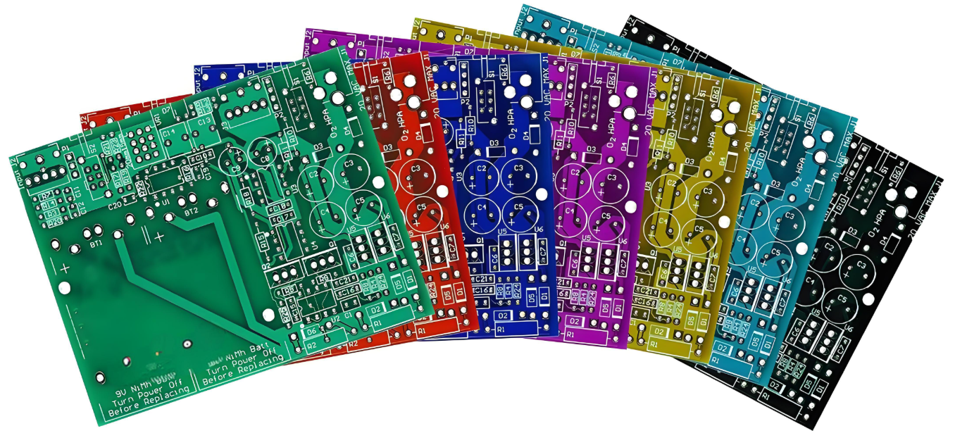
Purple circuit boards—also known as Purple PCBs—have become popular among makers, engineers, and even electronics brands that want to stand out. While the solder mask color doesn’t change how a PCB works, it does influence how it looks, feels, and even how it’s perceived.
In this blog, we’ll break down everything you need to know about Purple PCBs. You’ll learn where they shine, what benefits they offer, and when they’re worth the investment.
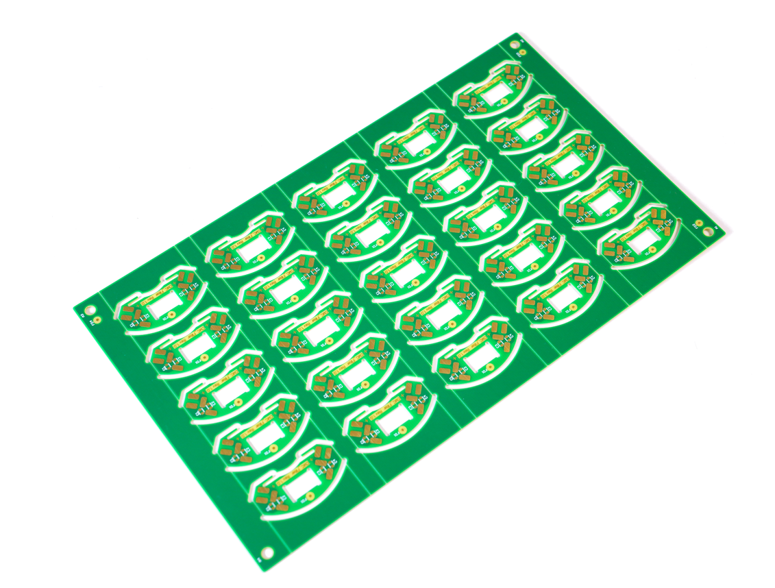
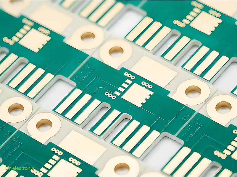
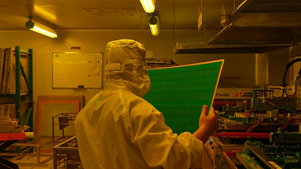
At EBest Circuit (Best Technology), we’ve been supporting product designers and OEMs with customized PCBs for years. From solder mask color to copper thickness and special surface finishes, we provide full manufacturing support. And yes—we proudly support purple solder mask PCBs.
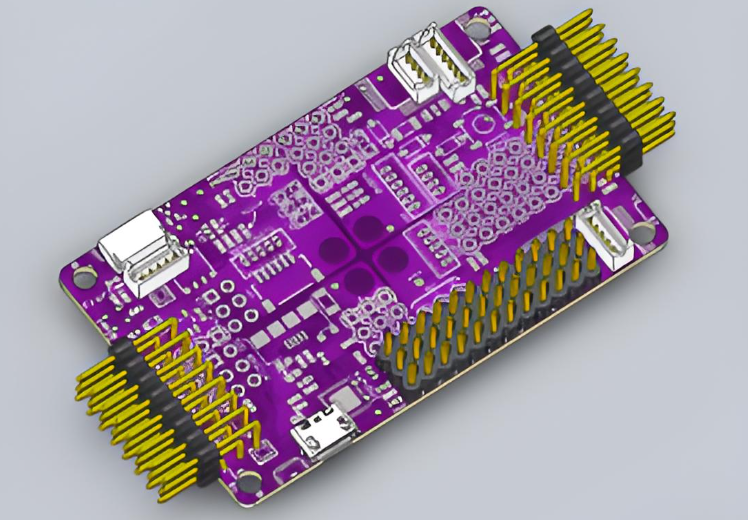
What is a Purple Circuit Board?
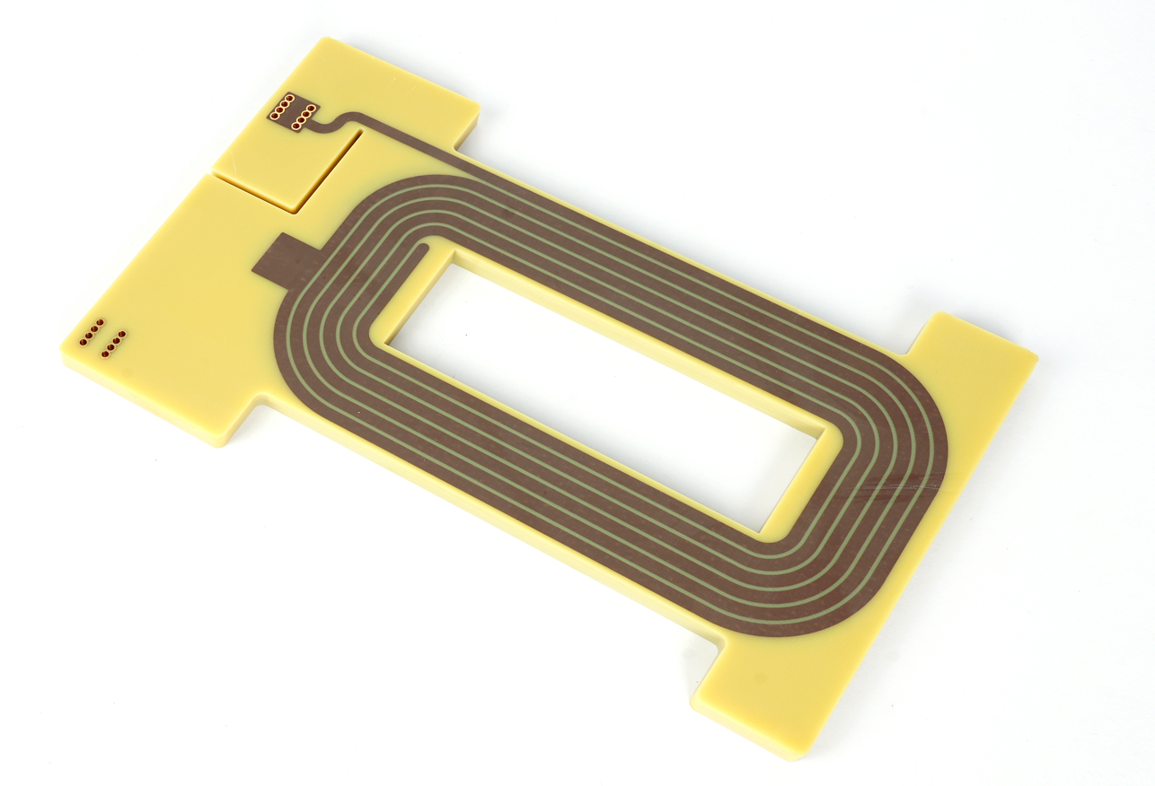
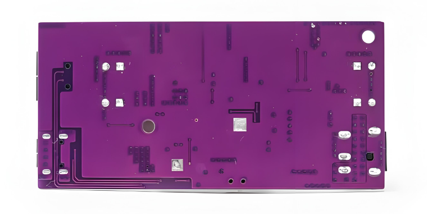
A purple circuit board is a printed circuit board that features a purple-colored solder mask. The solder mask is a thin protective layer applied over the copper traces of a PCB. Its job is to prevent oxidation, short circuits, and solder bridges during assembly.
While green is the most common color in PCB manufacturing, purple offers a unique visual twist. It’s not just a design choice—it’s a statement. Makers often associate purple PCBs with premium or small-batch electronics.
Some PCB manufacturers offer purple as a standard option. Others consider it a custom request. Either way, it doesn’t impact the electrical performance of the board. The difference is mostly visual and emotional.
Advantages of Purple PCB
Choosing a Purple PCB isn’t just about standing out—it can offer several practical and branding benefits too.
1. Unique Visual Identity
Purple PCBs are not commonly seen in mass-produced electronics. Using one helps your product stand out, especially if you’re building a niche device or showcasing your board.
2. Brand Recognition
Startups and makers often use purple solder masks as part of their brand identity. Think of it like choosing a unique color for your packaging—only this time, it’s part of the electronics.
3. Better Product Differentiation
If you’re producing multiple versions of the same board, using purple can help distinguish prototypes or special editions. You’ll never mix up versions during testing.
4. Enhanced Perceived Value
Because purple PCBs are less common, they give off a premium vibe. If your product has visible circuitry, purple adds to the appeal.
5. Maker Community Favorite
In the open-source and maker community, purple has almost become a symbol of small-batch craftsmanship. Platforms like OSH Park use purple as their signature color.
Purpose of Purple Circuit Board
The main purpose of a purple circuit board is to add visual distinction. In terms of function, it’s no different from any other PCB. But in terms of presentation, it stands out. Here’s where purple PCBs get used:
- Showcase prototypes at trade shows or demos
- Limited edition electronics with visible circuit boards
- Kickstarter campaigns where aesthetics add value
- Open-source hardware projects that are shared online
- Personal builds or portfolio projects
In all these cases, the purple color makes your design feel custom, creative, and intentional.
Does the Color of a Circuit Board Matter?
Functionally, no. A circuit board’s color doesn’t affect its electrical performance.
The solder mask color has no effect on signal transmission, current flow, or board durability. Whether you pick green, red, or purple, the functionality remains the same.
However, color does matter in other ways:
- Inspection Ease: Some colors, like green, offer better contrast for spotting solder bridges or defects.
- Heat Visibility: Black and dark boards retain heat, which may affect thermal visibility during rework.
- Aesthetic Value: If your PCB is visible to end users, color directly affects how it’s perceived.
So while purple won’t change how the board performs, it will change how it looks and how others interact with it.
What Are the Different Color Circuit Boards?
You can find PCBs in a variety of colors today. Here’s a look at the most common options and why you might choose them:
| Color | Why Choose It |
| Green | Industry standard, great contrast, cost-effective |
| Red | Easy to inspect, stands out from green, mid-cost |
| Blue | Aesthetically pleasing, often used in dev boards |
| Black | Sleek design, popular in high-end gadgets |
| White | Reflects light, good for LED boards |
| Yellow | Bright and easy to spot |
| Purple | Unique, stylish, excellent for branding |
Purple PCBs offer a perfect balance of visual uniqueness and readability, without being too flashy or difficult to inspect.
Which Color of Circuit Board is Better?
There’s no single “best” color—it depends on your project. But here’s how they generally compare:
- Best for Inspection: Green, Red
- Best for Consumer Products: Black, Blue
- Best for Lighting Applications: White
- Best for Branding and Style: Purple
If you care about cost, availability, and visual clarity, green is a solid default. If you care about product identity, purple is a strong contender. You can choose based on your end-use case, inspection needs, and visual goals.
When to Use Purple Circuit Board?
Consider using a Purple PCB if:
- You want to create a branded visual identity for your product.
- You’re making small batches where aesthetics matter.
- Your PCB is visible through a product’s casing.
- You need to visually differentiate between product versions.
- You’re working on a maker or educational project.
- You want to impress investors or early customers with a unique prototype.
If none of the above apply, and your board is hidden in an enclosure, you may not need purple. But if visibility, branding, or presentation are part of your plan, purple is a great choice.
Is Purple PCB More Expensive than Green Circuit Board?
Yes, purple PCBs usually cost more than green ones, but not by a large margin. The factors affect its cost are mainly:
- Material Availability: Green solder masks are stocked in bulk; purple is often a specialty item.
- Production Setup: Some fabricators treat purple as a custom order, which involves extra setup steps.
- Smaller Batch Runs: Purple PCBs are typically made in smaller quantities, which increases cost per unit.
That said, if you’re ordering a low to medium volume, the cost difference is generally affordable—especially considering the visual value. At EBest Circuit (Best Technology), we offer purple solder mask as an option without charging unreasonably high premiums. Ask us for a quote, and we’ll walk you through the pricing.
Methods for Producing Purple Solder Masks
Creating a purple solder mask on a printed circuit board can be achieved through two main techniques, each suited to different design and production needs:
1. Pigment-Mixed Solder Mask
In this method, purple pigments are directly blended into the liquid solder mask resin before it is applied to the board. This is especially effective with LED-curable solder masks, which allow for greater pigment flexibility compared to traditional UV-curable systems.
To ensure a rich and opaque purple finish, the mask layer may need to be slightly thicker. This additional thickness helps accommodate the pigment load and improves visual uniformity across the board surface.
2. Base Mask with Purple Legend Ink
This technique involves applying a base solder mask color, typically white, to the PCB. Purple legend ink is then printed over designated areas that require solder protection.
This approach offers vibrant purple color without significantly increasing mask thickness. It also enables the use of multiple colors on a single board, which is useful for custom designs or highlighting key areas. However, it demands precise registration during the legend printing process to maintain alignment and consistency.
Purple PCB Manufacturer – EBest Circuit (Best Technology)
At EBest Circuit (Best Technology), we are your reliable one-stop PCB manufacturer in China, ready to meet all your diverse circuit board needs—including custom Purple PCBs.
Our engineering, production, and quality teams bring years of experience across various industries. We understand that every sector has its own set of standards. Whether you’re in medical, automotive, or aerospace, we follow the most widely recognized industry practices to meet your exact requirements.
We manufacture all PCBs in compliance with IPC standards, including:
- IPC-A-600 for PCB fabrication
- IPC-A-610 for PCB assembly
By default, our products meet IPC Class 2 standards. If your application demands it, we also support Class 3 and Class 3A, which are common for high-reliability or mission-critical devices.
If you have any questions—whether it’s about pricing, MOQ, delivery times, certifications, quality standards, or engineering support—feel free to reach out at any time. Our team is here to help. We’re committed to becoming one of the best PCB manufacturers in China, focused on delivering the highest quality, competitive pricing, and dedicated service for every customer.
FAQs
1. Is purple solder mask just for looks?
Yes. Purple is a cosmetic choice. It does not change how the PCB works.
2. Can I use purple on high-frequency or HDI boards?
Absolutely. Purple solder masks are compatible with all types of PCBs, including multilayer, HDI, and RF boards.
3. Is purple solder mask more prone to defects?
No. As long as the process is controlled properly, purple performs just like other colors.
4. How can I get a purple PCB made?
Just mention the purple solder mask when you request a quote from us. We’ll confirm details and start the process.
5. Does EBest Circuit (Best Technology) offer other rare colors too?
Yes. Besides purple, we offer red, blue, yellow, black, white, and even custom Pantone shades.