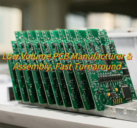
Why choose low volume PCB? Let’s explore meaning, benefits, applications, manufacturing and assembly processes, delivery time for low volume PCB.
Are you troubled with these problems?
- Waiting 48hours for a quote?
- Forced to order 10pcs when you need 2?
- Found silent tweaks in your Gerber files?
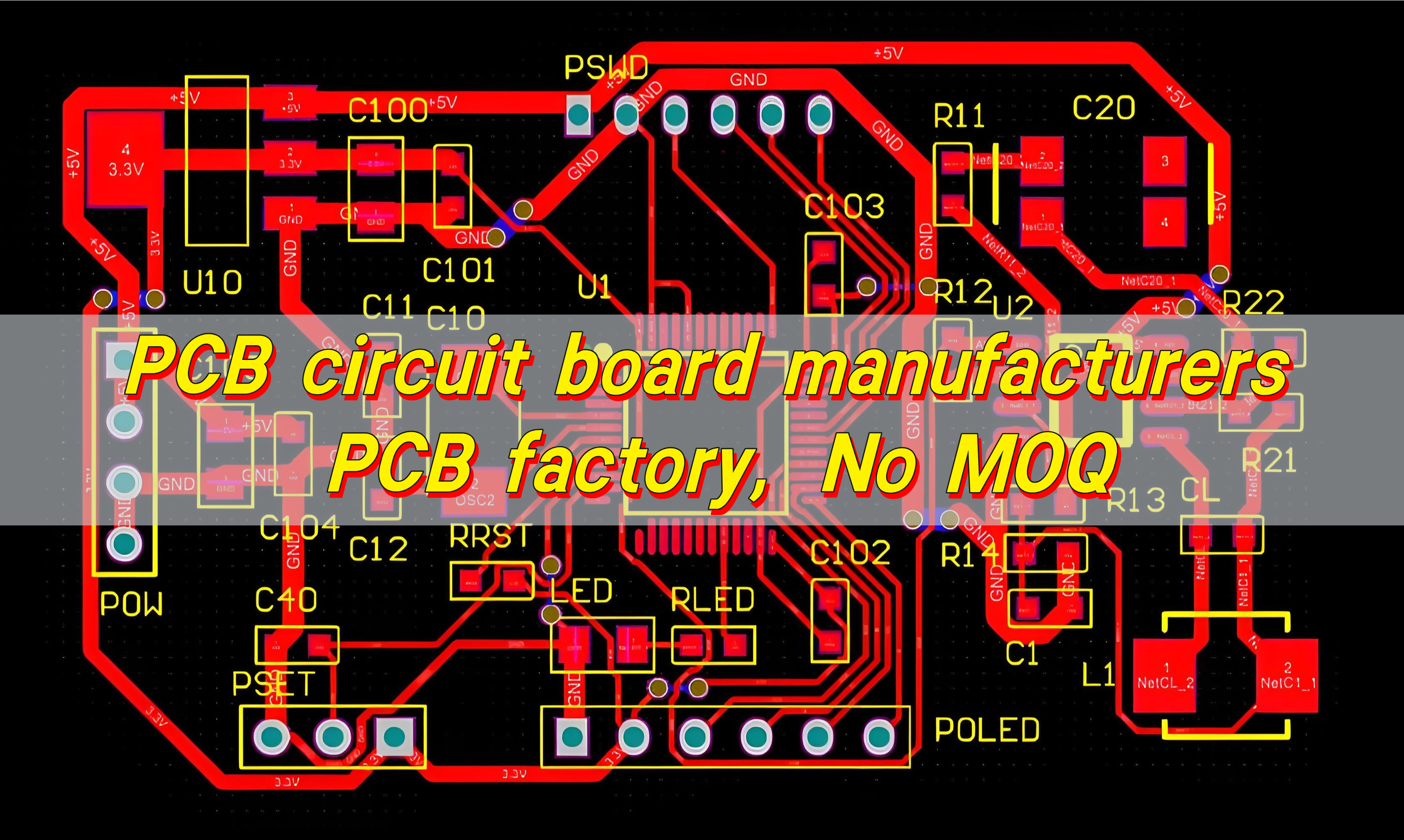
As a low volume PCB manufacturer, EBest Circuit (Best Technology) can provide you service and solution:
- Dedicated Project Ally – A single technical contact handles all needs 24/7, eliminating supplier runarounds.
- Order Just 1 Board – Pay only for materials used ($0 setup fees), with real-time cost breakdowns.
- Pre-Production DFM Analysis – Get actionable feedback within 12hrs. Your design intent stays uncompromised.
Welcome to contact us if you have any request for low volume PCB: sales@bestpcbs.com.
What Does Low Volume PCB Mean?
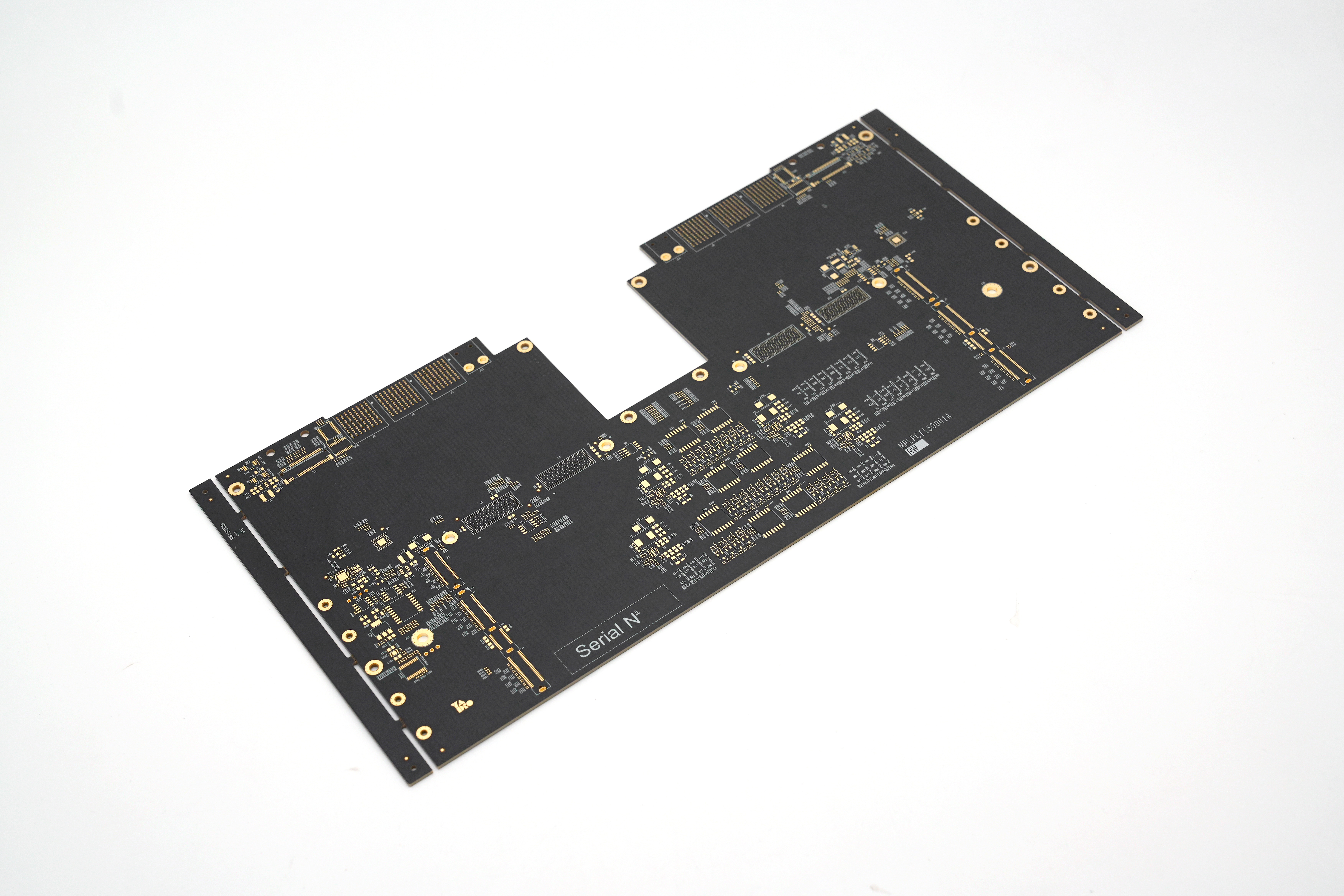
Low Volume PCB refers to a production model with single-order quantities typically ranging from 5 to 500 pieces, providing highly flexible manufacturing services for product R&D, prototype validation, and small-scale trial production. Unlike traditional mass production, it removes high mold fees and minimum order quantity restrictions, enabling rapid design iteration (e.g., design modifications within 48 hours), multi-process compatibility (e.g., high-frequency materials/HDI blind vias), and complex technical verification (e.g., ±5% impedance control).
Why Choose Low Volume PCBs?
Advantages of Low volume PCBs:
Lower upfront investment
- Avoid high tooling costs and material deposits.
- Ideal for limited R&D/startup budgets.
Faster design iteration
- Receive prototypes in 72 hours (vs. weeks for traditional manufacturing).
- Rapidly test and refine designs.
Flexibility for special requirements
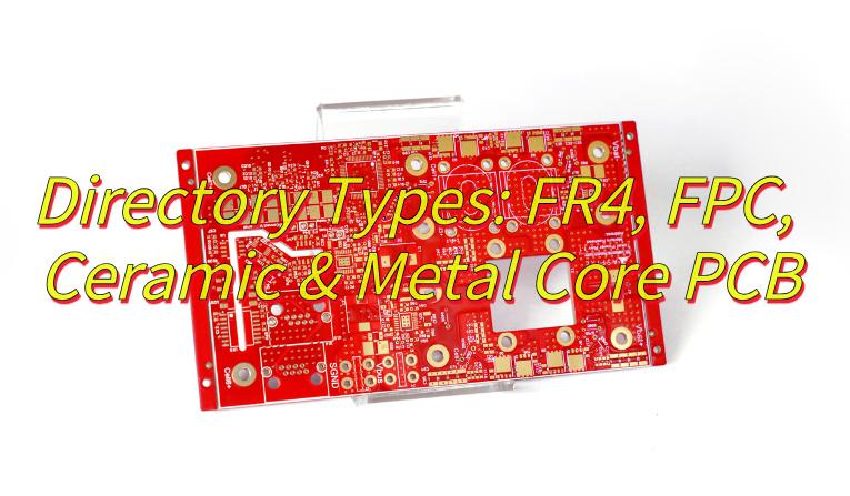
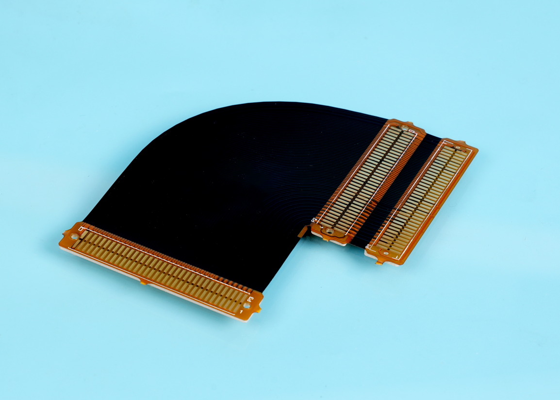
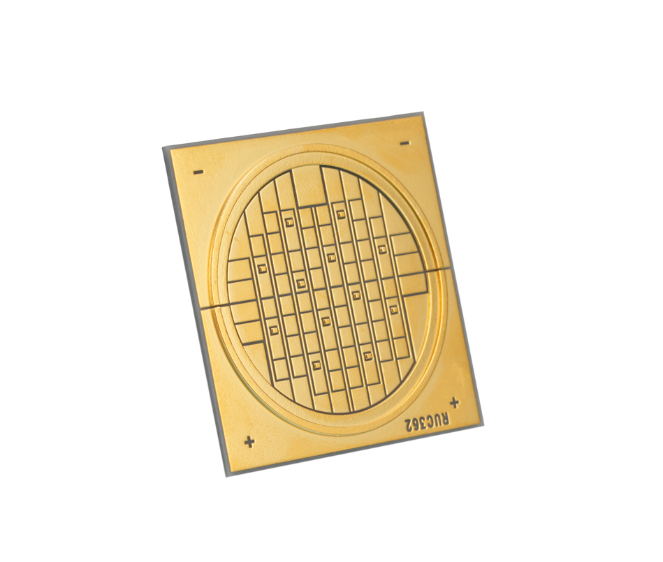
- Support niche materials (ceramic/flex PCBs).
- Accept customer-supplied components.
Enhanced quality control
- 100% manual inspection per board.
- Catch flaws before mass production.
Seamless market testing
- Launch pilot batches (100-500 units) for user validation.
- Customize labels/certifications per region.
When to Choose Low Volume PCB Board?
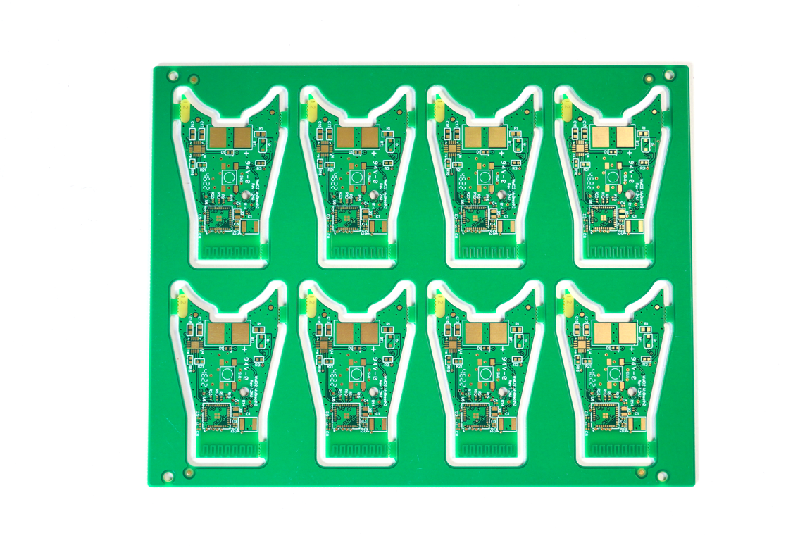
Applications of low volume PCB board:
- Smart Wearable Devices: Smart Watch, AR/VR Glasses.
- Medical Devices: Portable Monitor, High-Precision Surgical Instruments.
- Industrial Control Systems: PLC Controller, Industrial Robot Core Board.
- New Energy Vehicle BMS: Battery Management System.
- IoT Terminals: Smart Meters, Environmental Monitoring Nodes.
- Aerospace Special Circuit Boards: Satellite Control Modules, Radar Systems.
- Consumer Electronics: Robotic Vacuum Cleaners, Smart Door Locks.
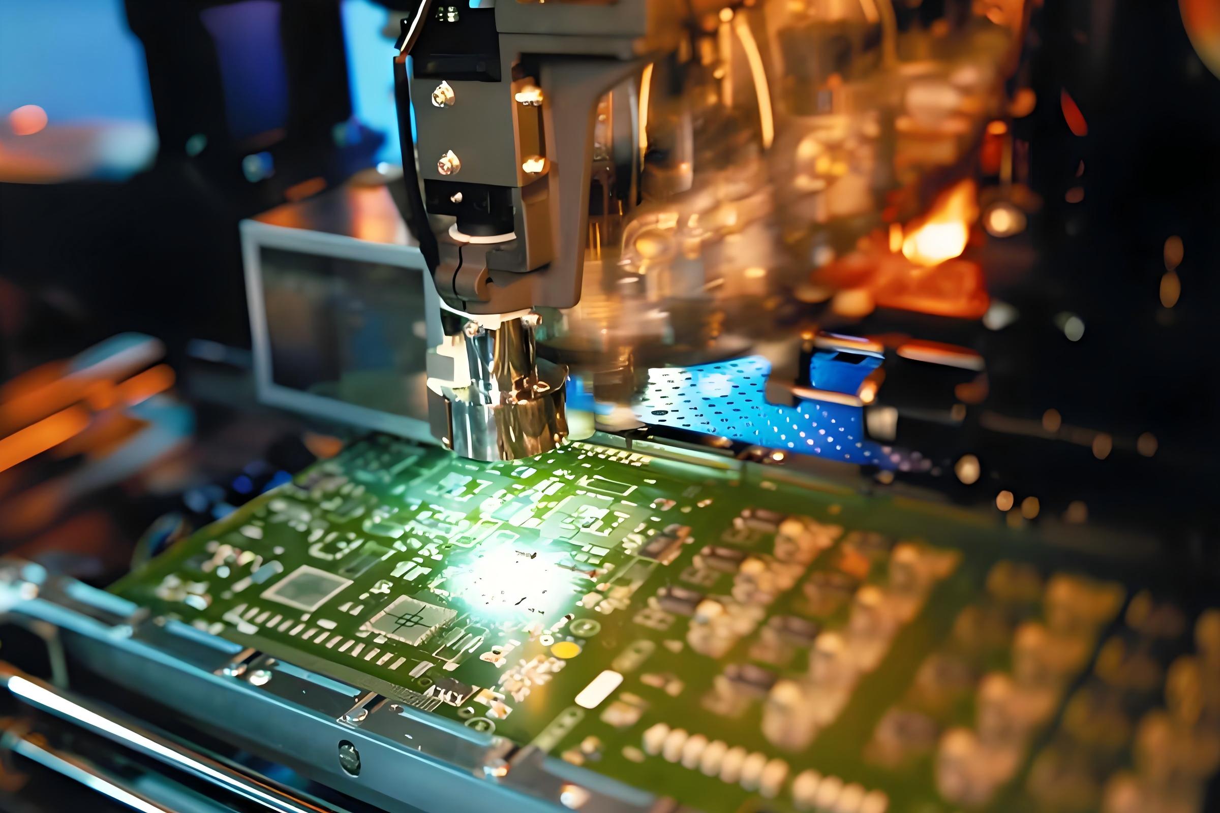
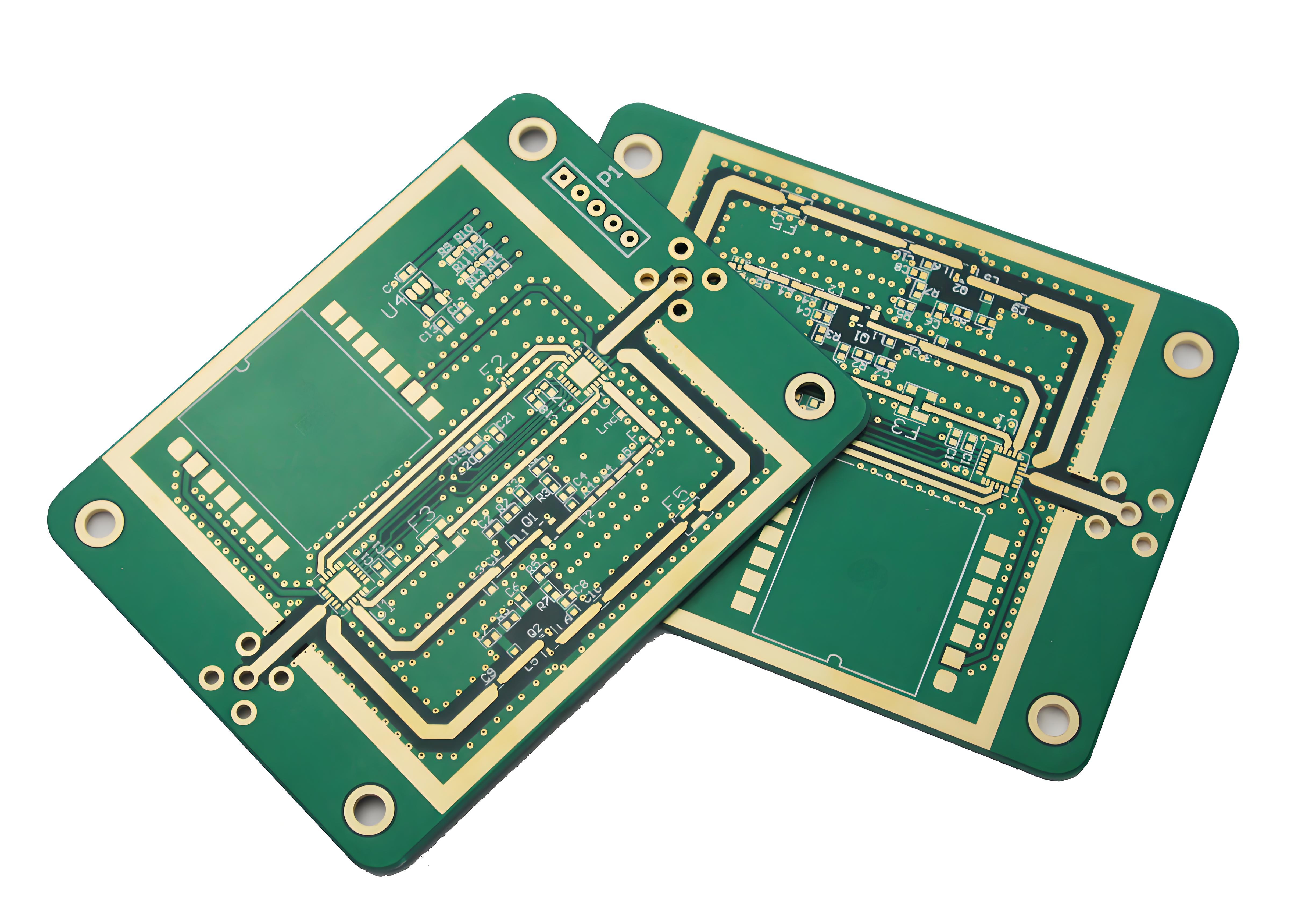
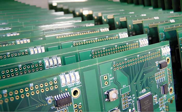
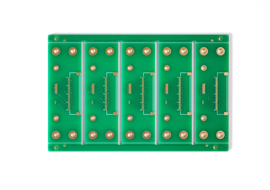
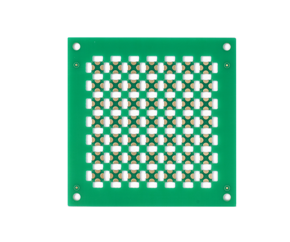
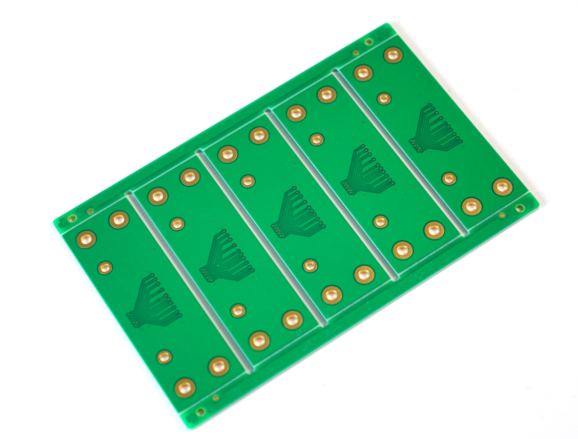
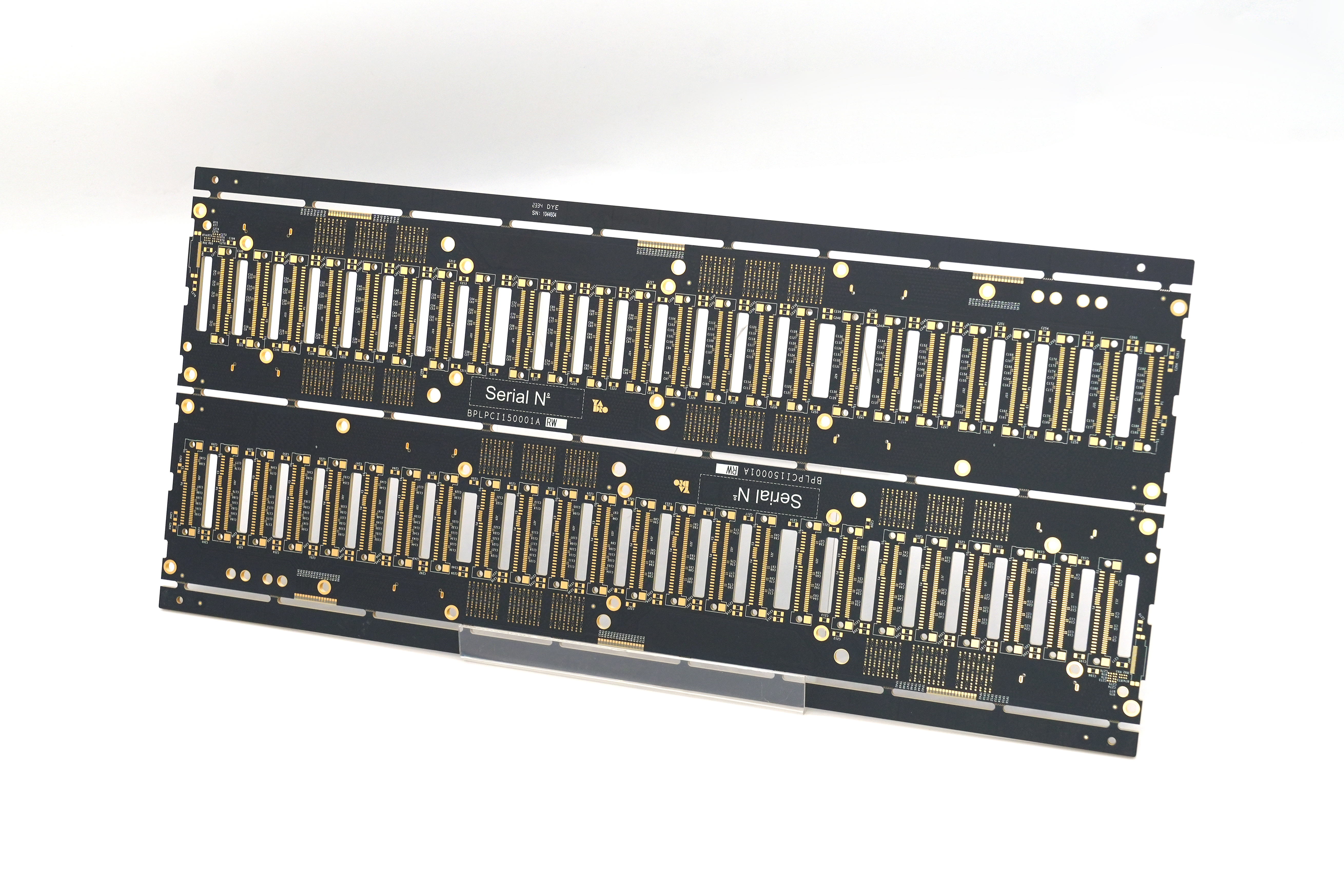
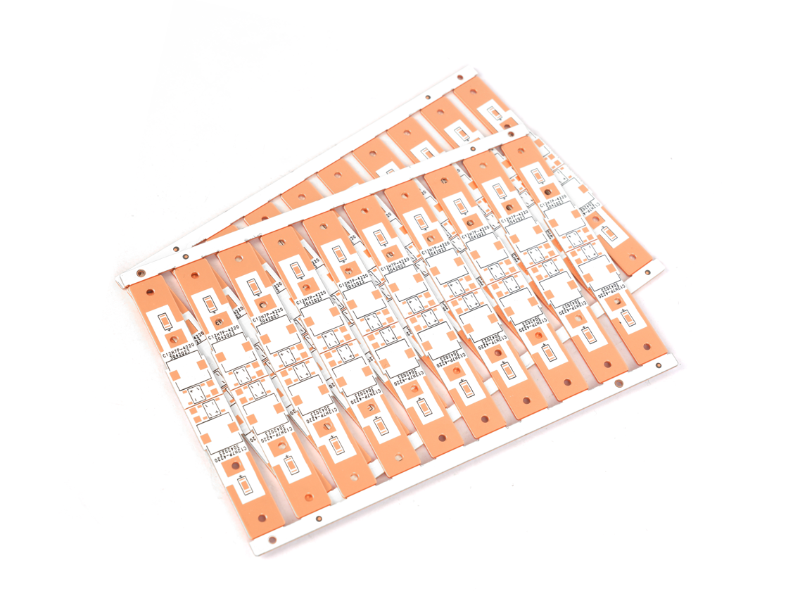
Low-Volume PCB Manufacturing Processes
1. Material Cutting: Large-size copper-clad laminates are cut to design dimensions, supporting small-batch multi-variety production and minimizing material waste.
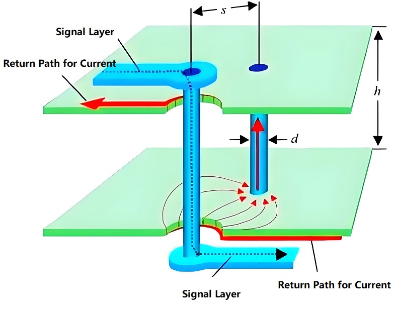
2. Drilling: CNC drilling machine creates through-holes/blind vias/buried vias with ±0.05mm hole position accuracy.
3. Hole Metallization: Chemical copper deposition + electroplating forms conductive layers for multi-layer board interlayer electrical interconnection.
4. Dry Film Lamination: Photosensitive dry film is applied to the board surface as a mask base for pattern transfer.
5. Pattern Exposure: UV exposure machine transfers Gerber file patterns to dry film, forming resist patterns.
6. Pattern Etching: Alkaline etching solution removes unprotected copper to form precise circuit patterns
Solder
7. Mask Printing: Liquid photosensitive solder mask ink is applied and developed to form a permanent protective layer.
8. Surface Finish: Immersion gold/OSP/ENIG and other processes enhance soldering reliability and corrosion resistance.
9. Profile Machining: CNC milling/laser cutting enables rapid shaping of irregular-shaped boards.
10. Electrical Testing: Flying probe/fixture testing completes 100% electrical performance verification, ensuring no shorts/opens.
11. Final Inspection: Manual visual inspection + AOI optical inspection double-verify appearance and dimensional compliance.
12. Packaging & Shipping: Anti-static vacuum packaging + anti-vibration cushioning materials, customized labels with batch/serial numbers, integrated logistics tracking system for full traceability

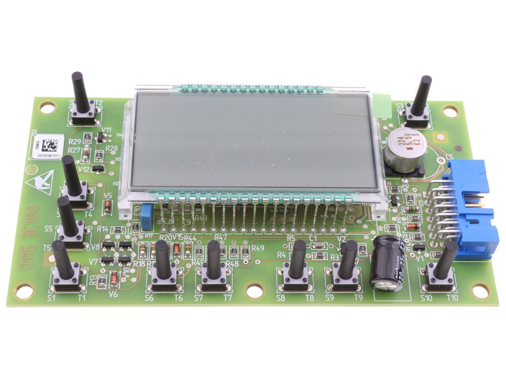
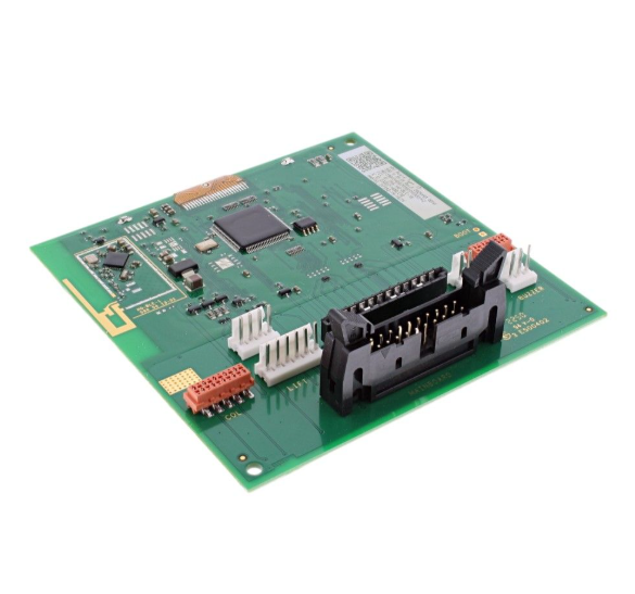
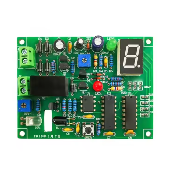
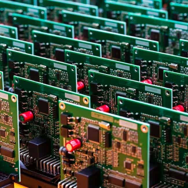
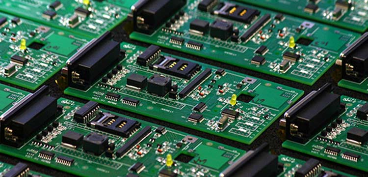
Low Volume PCB Assembly Processes
1. Component Preparation: Sorting and inspecting SMD/DIP components per BOM list, supporting small-batch multi-variety needs with rapid material switching capabilities.
2. Solder Paste Printing: High-precision stencil printing with ±0.02mm thickness control for uniform solder pad coverage.
3. SMD Placement: Modular pick-and-place machines enable high-speed precision mounting of micro-components (01005 chips, BGA packages).
4. Reflow Soldering: 10-zone nitrogen reflow oven achieves lead-free soldering with ±1°C temperature precision for reliable joints.
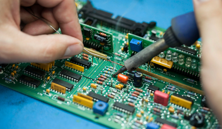
5. Through-Hole Assembly: Manual/automated insertion machines handle through-hole components, accommodating irregular shapes and precision placement.
6. Selective Soldering: Localized wave/selective soldering for through-hole parts minimizes thermal stress while ensuring consistent joint quality.
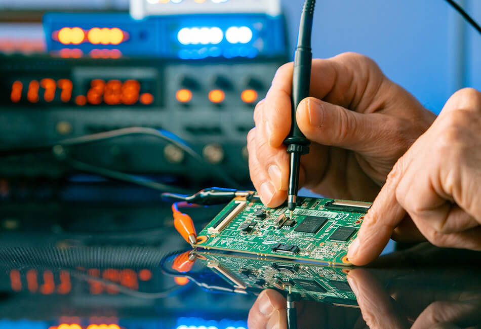
7. Functional Testing: ICT/FCT systems validate electrical performance, complemented by AOI/X-ray inspection for micro-defect detection.
8. Conformal Coating: Acrylic/silicone spray applied per requirements to enhance moisture/dust/corrosion resistance.
9. Packaging & Shipping: Custom anti-static packaging with cushioning materials, integrated logistics tracking for secure and traceable delivery.
Why Choose EBest Circuit (Best Technology) as Low Volume PCB Manufacturer?
Reasons why choose us as low volume PCB manufacturer:
- One-Stop Solution: Full-link service covering PCB design to assembly, eliminating the need for clients to coordinate with multiple suppliers. Reduces R&D cycle by over 30% and lowers cross-department communication costs.
- Free DFM Design Optimization: 19-year experienced engineering team provides Design for Manufacturing (DFM) analysis to identify design flaws early, minimize subsequent modification costs, improve first-board success rate by 40%, and avoid rework losses in mass production.
- 19 Years of Experience Accumulation: Focused on low-volume PCB production, serving over 2,000 clients. Rich process database enables rapid adaptation to complex process requirements, ensuring enhanced production efficiency and yield.
- Four-Layer Quality Control System: Incoming material inspection, in-process patrol inspection, 100% final product inspection, and reliability testing. Achieves full batch inspection with defect rate below 0.3%, significantly outperforming industry averages and ensuring product reliability.
- Dynamic Cost Optimization Solutions: Customized cost-reduction strategies based on client budgets, including material substitution, process adjustments, and batch pooling. Reduces costs by 15%-30% while maintaining quality, maximizing cost-effectiveness.
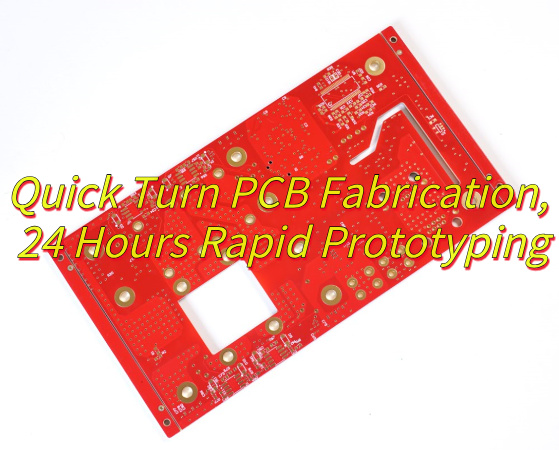
- 24-Hour Rapid Prototyping: 24-hour expedited prototyping for double-sided boards, 3-day delivery for 4-6 layer boards, 50% faster than conventional timelines. Accelerates design validation and market entry.
- Flexible Production Scheduling: Dedicated production lines support small-batch orders starting at 50 pieces. Intelligent scheduling system enables rapid line changes (under 2 hours), flexibly accommodating multi-version and multi-batch production needs.
- Professional Assembly Support: Comprehensive assembly services including SMT placement, DIP insertion, and conformal coating. Combined with precise soldering temperature curve control and solder joint inspection, ensures component assembly accuracy of ±0.025mm and stable electrical performance.
Our Low Volume PCB Lead Time
Lead time for 1-50 pieces
| Layers | Normal Service | Fastest Service |
| 1 | 7 Days | 24 H |
| 2 | 8 Days | 24 H |
| 4 | 10 Days | 48 H |
| 6 | 10 Days | 72 H |
| 8 | 12 Days | 72 H |
| ≥10 | TBD | TBD |
Lead time for 50-500 pieces
| Layers | Normal Service | Expedited Service |
| 1 | 4-6 Days | 2-3 Days |
| 2 | 5-8 Days | 2-3 Days |
| 4 | 8-12 Days | 3-5 Days |
| 6 | 8-12 Days | 4-6 Days |
| 8 | 12-16 Days | 6-8 Days |
| ≥10 | 18-20 Days | TBD |
How to Get a Quote for Low Volume PCB Project?
Essential Quote Submission Checklist for Low Volume PCB Projects
- Design Data: Complete Gerber files (274X, NC Drill) with layer-specific details (dimensions, copper thickness, via specs).
- BOM: Detailed component list with part numbers, manufacturers, quantities, and critical component flags.
- Technical Specs: PCB layer count, material type (e.g., FR4, high-Tg), surface finish (ENIG/HASL/OSP), impedance targets, and special processes (HDI, blind vias).
- Quantity & Timeline: Annual/batch volume and required delivery dates (prototypes to mass production).
- Quality Standards: IPC-A-600/A-610 compliance, reliability tests (thermal cycling, vibration), and certifications (RoHS, UL).
- Assembly Needs (If Applicable): SMT/DIP specs, solder paste type, test protocols (ICT/FCT), and coating requirements.
Welcome to contact us if you have any inquiry for low volume PCB design, manufacturing, assembly: sales@bestpcbs.com.