How to choose PCB manufacturing Brisbane? This blog is about benefits, types, quality requirement, factory list and selection guide for PCB manufacturing Brisbane.
Why Choose PCB Manufacturing Brisbane?
Advantages of PCB Manufacturing Brisbane:
- Local Rapid Response: Brisbane PCB manufacturers offer local technical support, enabling problem feedback and solutions to be completed within 24 hours, minimizing project delay risks.
- Strict Quality Control: Adopt ISO-certified manufacturing processes and AOI optical inspection technology to ensure stable electrical performance and a defect rate below 0.3% per batch, meeting international standards.
- Customized Cost Optimization: Provide tiered pricing for small and medium batch orders, leveraging local supply chain advantages to reduce shipping and tariff costs, saving 15%-20% in comprehensive expenses compared to overseas manufacturing.
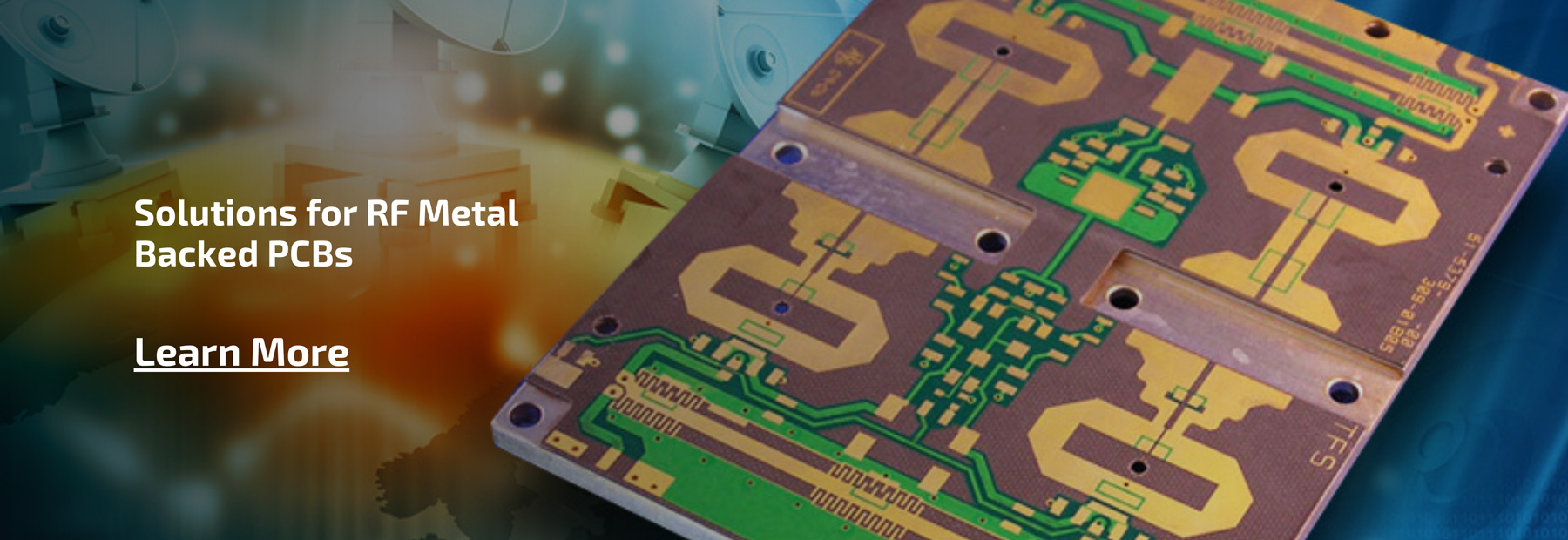
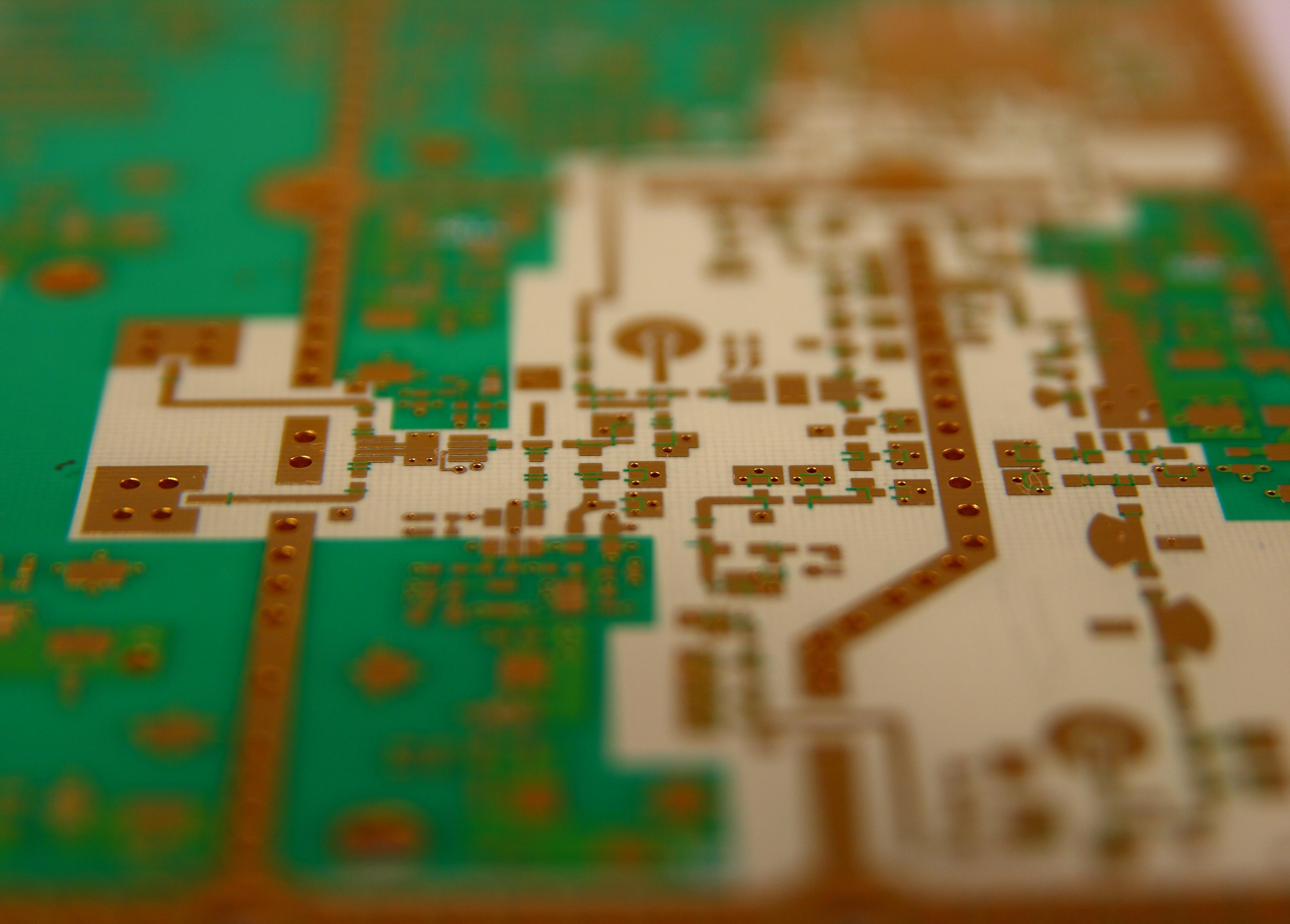
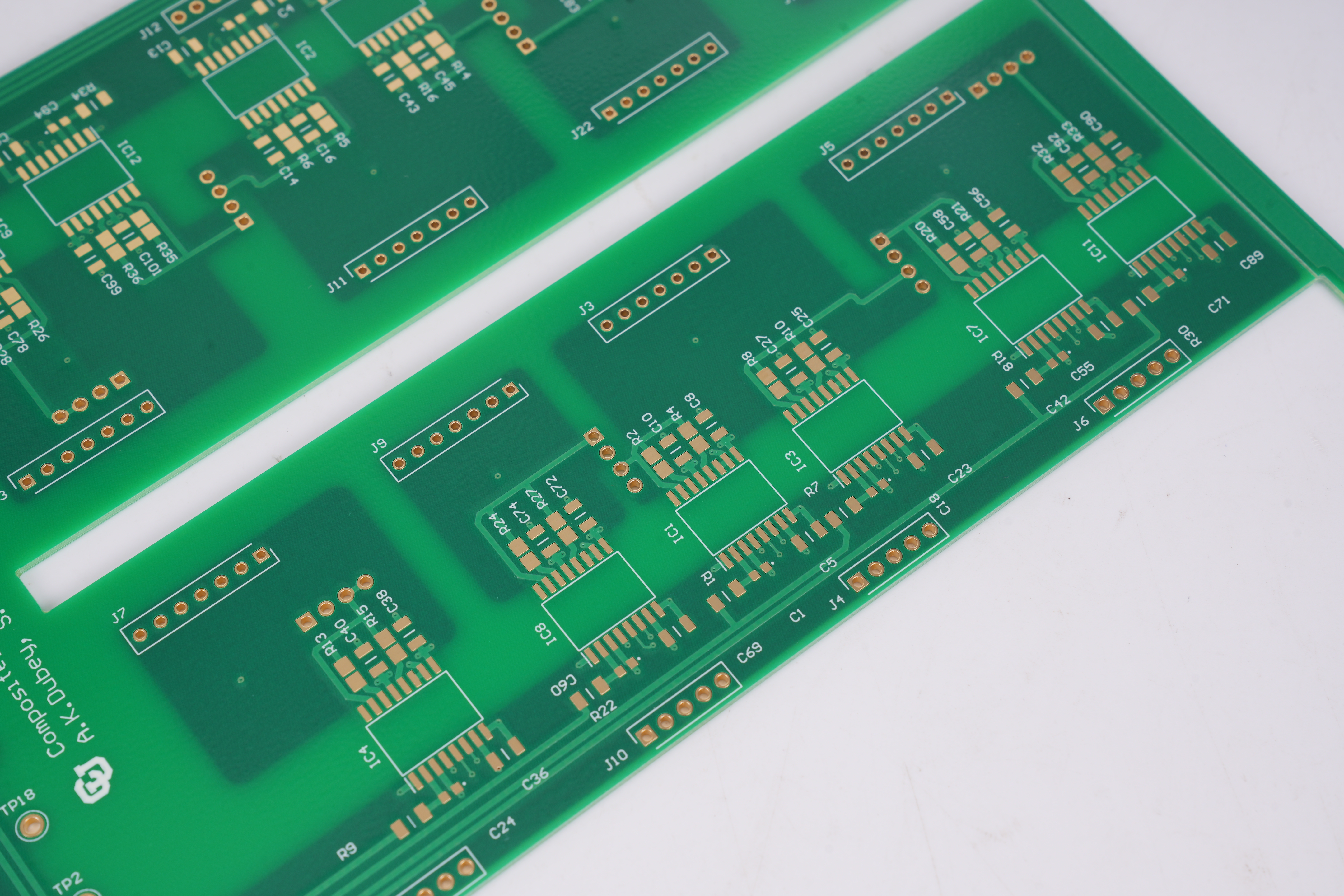
- Strong Technical Adaptability: Support processing of high-density interconnect (HDI), flexible circuits (FPC), and specialty substrates (such as high-frequency ceramics), meeting the needs of cutting-edge fields like 5G, medical, and automotive electronics.
- Environmental Compliance Guarantee: Utilize lead-free processes and recyclable materials throughout, complying with RoHS, REACH, and other environmental regulations to avoid compliance risks during product export.
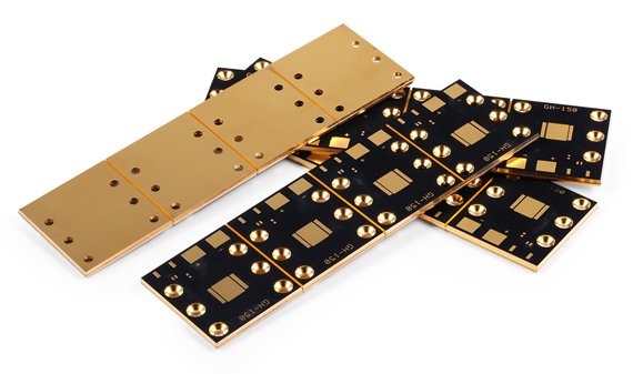
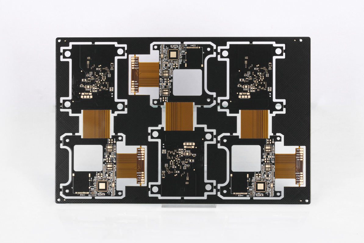
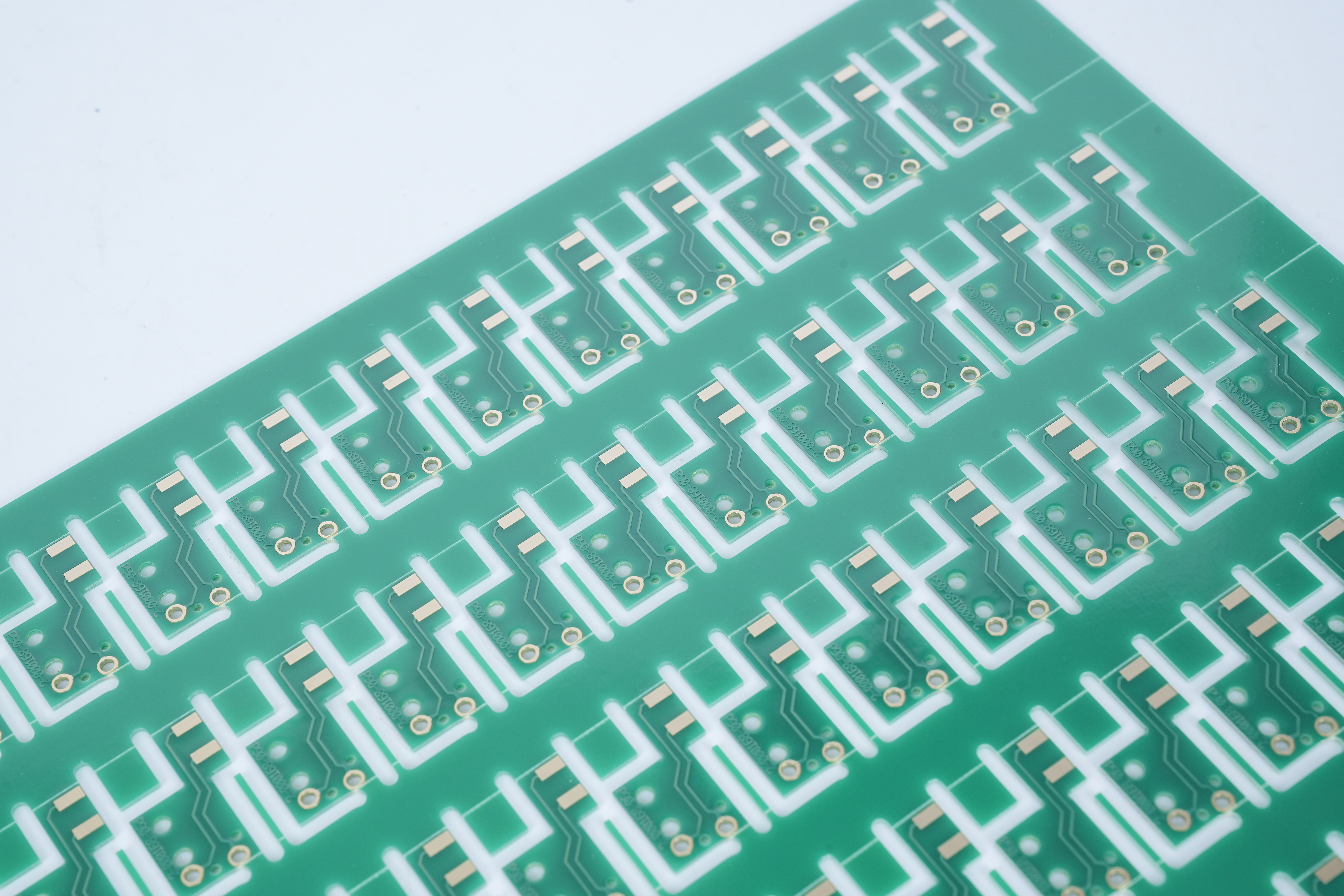
Types of PCB Manufacturing Brisbane
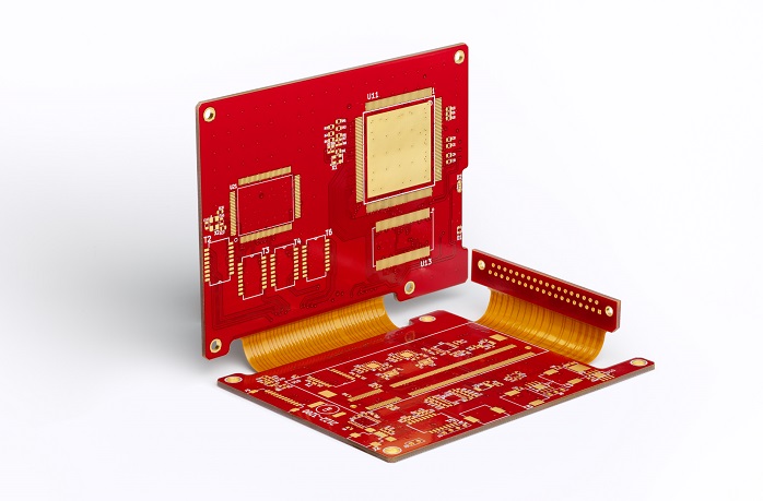
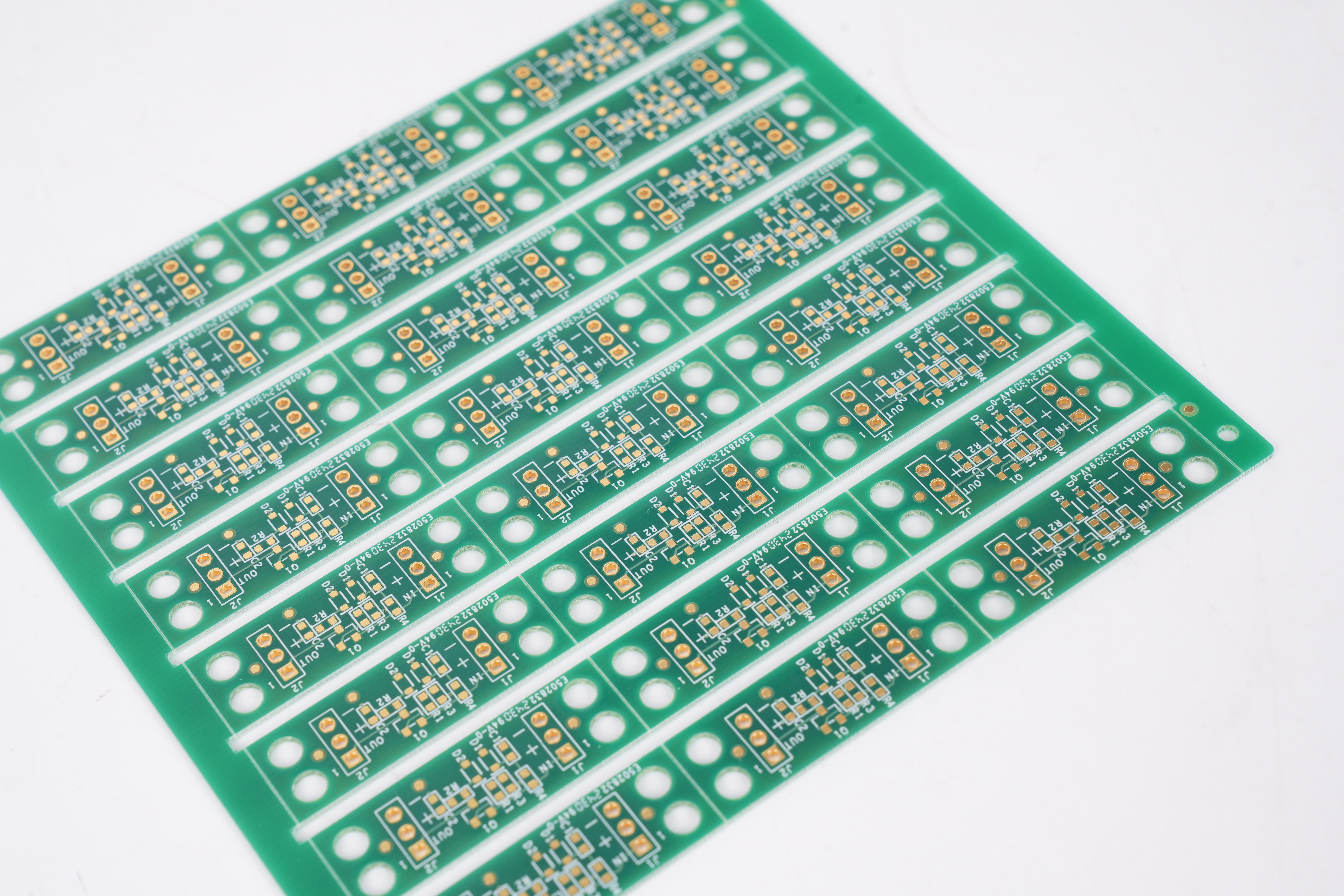
- Rigid PCB
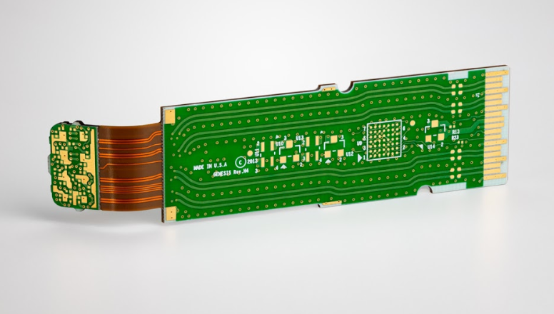
- Flexible PCB
- Rigid-Flex PCB
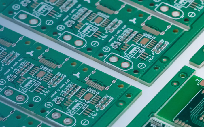
- Single-layer PCB
- Double-layer PCB
- Multi-layer PCB
- HDI PCB
- High-frequency PCB
- Metal-core PCB
- Heavy Copper PCB
- Ceramic PCB
- High TG PCB
- Halogen-free PCB
Quality Certifications for PCB Manufacturing Brisbane
- ISO 9001 Quality Management System Certification: Ensures that companies establish a standardized quality management system covering the entire process of product design, production, and testing, guaranteeing that products meet customer requirements and regulatory standards.
- ISO 14001 Environmental Management System Certification: Regulates waste disposal, energy consumption control, and the use of environmentally friendly materials in the production process, reducing pollution to soil, water, and air.
- SAA Certification: Focuses on electrical safety, requiring products to undergo overload, insulation, and grounding tests by Australian accredited laboratories (such as NATA), and to bear the SAA mark.
- RCM Certification: Integrates electrical safety and electromagnetic compatibility (EMC) requirements, covering electronic products (such as power adapters and LED lighting). It replaced A-Tick/C-Tick in 2016 and is the Australian market access mark.
- UL Certification: Verifies the electrical safety, material flame retardancy (such as UL 94 V-0 rating), and mechanical stability of PCBs, preventing safety hazards such as fires.
- RoHS: Restricts the use of six hazardous substances, including lead, mercury, and cadmium, in electronic products.
- REACH: Manages the entire lifecycle of chemicals, requiring companies to declare and restrict the content of substances of very high concern (SVHCs).
- IATF 16949: Automotive electronics PCB standard, strengthening specific requirements for the automotive industry (such as high reliability and traceability).
- ISO 13485: Medical device PCB standard, focusing on the safety, effectiveness, and quality management system of medical devices.
- AS9100D: Aerospace PCB standard, covering stringent requirements for materials, processes, and testing.
- IPC-A-600/6012: Defines PCB appearance, dimensions, layering, and performance specifications, ensuring compliance with electronic assembly acceptability standards.
- IPC-J-STD-001: Specifies welding process and material standards, ensuring the reliability of electrical connections.
Top PCB Factory in Brisbane List
| PCB Factory | Main Business | Advantages | Production Capability | Typical Lead Time |
| Brisbane Circuits | Prototype PCBs, small-batch FR4 PCBs, 2–6 layers | Stable communication, flexible prototype support, smooth DFM help | Line width/space 5/5 mil, BGA 0.4 mm, 2–6 layers | 3–7 days for prototypes |
| Queensland PCB Solutions | Multi-layer PCBs, industrial control PCBs, PCBA | Strong assembly team, neat workshop, fast test setup | 4–10 layers, mixed assembly, ICT & FCT | 7–10 days PCB, 10–14 days PCBA |
| Brisbane RF & Microwave Lab | RF PCB, high-frequency PCB, Rogers materials | Good impedance control, trained RF engineers | RO4003C, RO4350B, 6–8 layers, ±8% impedance | 7–12 days |
| SmartBuild Electronics Brisbane | HDI PCB, IoT module integration, turnkey services | Simple ordering flow, good revision tracking | Microvias 0.1 mm, HDI 1+N+1, stack-ups for compact devices | 8–12 days |
| TechEdge Manufacturing Brisbane | Medium-volume PCB mass production, PCBA | Stable line control, quality systems, RoHS compliance | 2–8 layers, SMT + THT, X-ray for BGAs | 10–18 days for batches |
| EBest Circuit (Best Technology) (China + Vietnam) | PCB + PCBA for global clients, RF PCB, HDI PCB, ceramic PCB | Professional engineering team, ISO9001/ISO13485/IATF16949/AS9100D, strong RF/HDI experience, MES traceability, competitive pricing, stable supply | 1–40 layers, HDI 1+N+1 / 2+N+2, 0.07 mm microvias, Rogers + ceramic materials, SMT line in China & Vietnam | 2–7 days prototypes, 10–15 days batches, 7–12 days global shipping to Brisbane |
How to Identify a Reliable PCB Factory in Brisbane?
Below Is An Identification Guide for PCB Factory in Brisbane:
1. Verify Certifications & Industry Standards Compliance
- ISO 9001/AS9100/IPC-A-610: Ensure factories hold ISO 9001 (quality management) and AS9100 (aerospace-grade) certifications. Brisbane’s Circuit Solutions Pty Ltd and Lintek Pty Ltd meet these standards, ensuring adherence to IPC-A-610 (bare PCB acceptability) for defect-free production.
- RoHS Compliance: Confirm lead-free manufacturing (e.g., Rush PCB Australia’s RoHS-certified processes) to align with global environmental regulations.
2. Audit Quality Control Processes
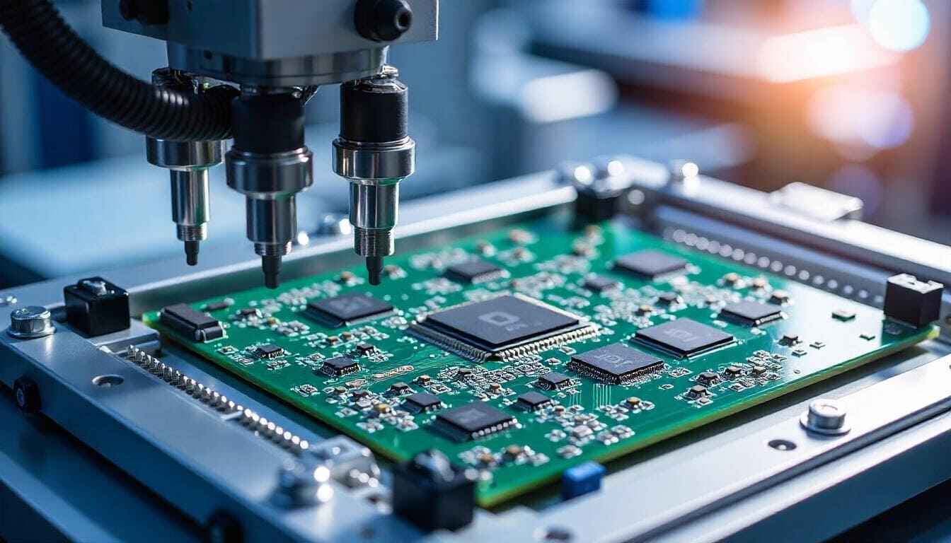
- Inspection Technologies: Prioritize factories using AOI (Automated Optical Inspection), Fly Probe Testing, and X-ray inspection (e.g., OurPCB Australia) for 100% solder joint integrity.
- AQL (Acceptable Quality Level): Demand statistical process control with strict defect limits (e.g., 0.1mm trace/space tolerances at COLETEK) to minimize rework risks.
3. Evaluate Manufacturing Capabilities
- Equipment & Materials: Look for advanced tools like LDI (Laser Direct Imaging) for precision traces (<0.1mm), multi-layer capabilities (up to 24 layers), and support for high-Tg/Rogers materials.
- Design for Manufacturability (DFM): Factories offering free DFM checks (e.g., Gold Coast Electronics) reduce prototyping costs by flagging design flaws early.
4. Assess Turnaround Times & Flexibility
- Prototyping Speed: Optimize for factories with 24-48 hour prototype delivery for rapid iteration. Standard production should align with your timeline (12–14 days for volume orders).
- Scalability: Confirm high-volume capacity (e.g., B.E.C. Manufacturing’s SMT lines) without compromising quality.
5. Review Customer Testimonials & Case Studies
- Trust Signals: Seek client reviews highlighting technical support responsiveness (e.g., Taylormade Electronics’ “prompt communication” with Cameron) and defect-free performance in demanding applications (e.g., mining equipment PCBs lasting 3+ years).
- Case Studies: Analyze projects like Multistore Industries’ 3D handle prototype (completed in 1 week by COLETEK) to gauge problem-solving agility.
6. Check Environmental & Sustainability Practices
- Waste Reduction: Prioritize factories with recycling programs (e.g., Lintek Pty Ltd’s patented High Vacuum Deposition process minimizes material waste) and energy-efficient production (e.g., Rush PCB Australia’s carbon footprint reduction).
7. Evaluate Technical Support & Transparency
- Real-Time Communication: Factories offering online portals for order tracking (e.g., Circuit Solutions Pty Ltd) or direct engineering consultations (e.g., COLETEK’s robotics expertise) reduce project delays.
- Transparent Pricing: Avoid hidden fees by selecting suppliers with upfront quotes and bulk discount eligibility (e.g., Gold Coast Electronics’ “no hidden fees” policy).
8. Assess Warranty & After-Sales Support
- Warranty Terms: Confirm clear warranty periods (e.g., 1–2 years for defect coverage) and responsive after-sales service. Factories like QualiEco Circuits are renowned for on-time delivery and post-production support.

How to Evaluate the Manufacturing Capability of PCB Factory in Brisbane?
Evaluation Methods About Manufacturing Capability of PCB Factory in Brisbane:
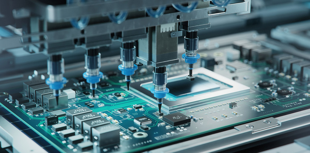
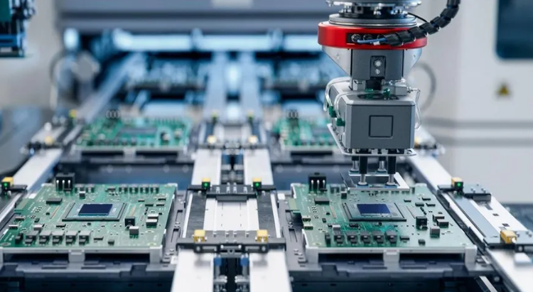
1. Core Equipment & Technical Capabilities
- Precision Process Capabilities: High-density routing (line width/spacing below 50μm), production of 20+ layer multilayer boards, specialized processes (HDI blind/buried vias, rigid-flex PCBs).
- R&D Innovation & Capabilities: R&D investment ≥10% revenue, patent portfolio, e.g., 5G high-frequency PCBs, AI chip substrates, DFM analysis capabilities.
2. Quality Control & Inspection Systems
- Full-Process Quality Management: ISO 9001 certification, raw material inspection (e.g., copper clad laminate, solder), AOI/X-ray inspection, flying probe testing, ICT.
- Critical Process Control: SPC for process monitoring, signal integrity simulation for final validation.
3. Material Management & Supply Chain Synergy
- Inventory & Logistics Efficiency: ERP system integration, inventory turnover rate, material shelf-life monitoring, anti-mixing mechanisms.
- Supply Chain Resilience: Supplier partnership stability, rapid response to urgent orders, flexible production capabilities.
4. Environmental Compliance & Sustainable Development
- Regulatory Adherence: RoHS 2.0, REACH, lead-free solder compliance, VOC emission control, segregated wastewater treatment.
- Green Manufacturing: Halogen-free substrates, low-VOC inks, laser soldering, energy-efficient processes.
5. Engineering Support & Service Responsiveness
- Design Collaboration: DFM feedback, impedance control (90±10Ω), thermal management solutions.
- After-Sales Traceability: Batch traceability system, rapid issue localization, NDA compliance.
How to Evaluate the Lead Time of PCB Factory in Brisbane?
Evaluation Methods About Lead Time of PCB Factory in Brisbane:
1. Pre-Production Readiness
- Design Validation Time: Assess how quickly the factory reviews and validates Gerber files, ensuring DFM (Design for Manufacturing) feedback is provided within 24-48 hours. Rapid prototyping capabilities (e.g., 2-layer boards in 3-5 days) signal efficiency.
- Material Sourcing: Confirm availability of core materials (FR4, Rogers) and specialty substrates. Short lead times depend on local/offshore supplier networks—local suppliers reduce logistics delays.
2. Production Process Efficiency
- Layer Stacking & Imaging: Evaluate automation levels in imaging, etching, and drilling. Factories with automated lines reduce manual errors and speed up processes (e.g., 4-layer boards in 5-7 days).
- Throughput Capacity: Inquire about daily/weekly output capacity. Factories with flexible shifts or parallel production lines accommodate urgent orders without compromising quality.
3. Post-Production Handling
- Quality Assurance (QA): Check QA protocols, AOI, flying probe, and electrical testing. Streamlined QA processes (24-48 hours) prevent delays.
- Packaging & Logistics: Review packaging standards (ESD-safe) and shipping partnerships. Brisbane-based factories offer local delivery (1-3 days) or international shipping (5-10 days via air freight).
4. Communication & Transparency
- Order Tracking Systems: Prioritize factories with real-time order portals or dedicated account managers for updates. Clear communication prevents misalignment on deadlines.
- Historical Performance: Request case studies or client testimonials highlighting on-time delivery rates. Consistency in meeting deadlines builds trust.
5. Customization & Scalability
- Small-Batch vs. Volume Orders: Understand how lead times scale with order size. Small batches (5-100 units) may take 5-7 days; volumes (1,000+ units) require 10-15 days.
- Rush Order Policies: Confirm availability of expedited services (24-hour turnaround for prototypes) and associated costs.

Frequently Asked Questions of PCB Manufacturing Brisbane
Q1: What is the typical turnaround time for PCB manufacturing in Brisbane?
A1: Prototype orders typically take 3–7 working days, small production batches 7–12 days, and complex designs (e.g., HDI/RF) 10–15 days. For urgent needs, some engineers pair local factories with global suppliers offering 2–7 day prototypes and fast shipping to Brisbane.
Q2: Do Brisbane PCB manufacturers support high-frequency/RF materials like Rogers?
A2: Availability varies; some labs process RO4003C/RO4350B, but options may be limited. Buyers often choose suppliers with full Rogers ranges (e.g., RO3003, RO5880) and pre-production DFM support for impedance tables and stack-up advice.
Q3: Are PCB assembly services (PCBA) available locally?
A3: Yes, several Brisbane companies offer SMT/THT assembly with BGA support and optical inspection. However, turnkey solutions (component sourcing, X-ray for BGAs, mixed-volume assembly) are often provided by suppliers with integrated PCB+PCBA+testing flows and MES tracking.
Q4: How to verify a factory’s capability for design tolerances?
A4: Check minimum trace/space (typically 4/4–5/5 mil), drill sizes, microvia capacity, impedance control (±10% common), and material/stack-up libraries. For HDI/fine-pitch/RF designs, request a DFM review to identify risks early.
Q5: Is Brisbane PCB manufacturing cost-effective for prototypes?
A5: Local prototype costs are higher due to labor/facility expenses, but early prototypes are often built locally for convenience. Later stages may shift overseas. Suppliers with low MOQ, competitive pricing, and DDP shipping to Australia help balance cost and predictability.