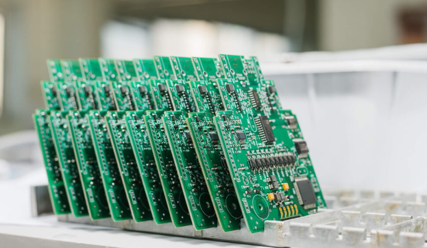
When you search for a professional, reliable, and certified PCB manufacturer in Cambodia, you need a partner that delivers consistent quality, on‑time delivery, full regulatory compliance, and end‑to‑end manufacturing support. Established in 2006, EBest Circuit (Best Technology) is a trusted PCB manufacturer in Cambodia with over 20 years of experience serving global buyers in automotive, medical, aerospace, industrial, consumer electronics, and communications markets. We specialize in custom PCB manufacturing, rapid prototyping, mass production, and turnkey PCB assembly, helping engineering, procurement, and production teams reduce risks, accelerate product launches, and stabilize supply chains.
Why Choose EBest as Your Trusted PCB Manufacturer in Cambodia?
When you partner with EBest, you gain more than a supplier, you get a dedicated manufacturing partner focused on your success. We prioritize your lead times, quality, compliance, and total project efficiency.
- On-time delivery guaranteed: Expedited orders ship in 24 hours; mass production strictly follows committed schedules to keep your project on track.
- Stable, repeatable quality: Full-process inspection and automated production minimize defects and ensure consistency in every batch.
- Complete global certifications: IATF 16949, ISO 9001, ISO 13485, AS9100D, REACH, RoHS, UL, fully compliant for automotive, medical, aerospace, and industrial markets.
- Customization & free support: Custom PCB design & manufacturing with free DFM analysis to optimize your design, lower failure rates, and avoid production delays.
- Flexible MOQ & service: Low minimum order quantity for prototypes; personalized support for small-batch R&D and large-scale mass production.
- Full component & assembly support: One-stop service eliminates coordination hassle and shortens your overall supply cycle.
Our Full-Service PCB Solutions as a Leading PCB Manufacturer in Cambodia
As a premier PCB manufacturer in Cambodia, EBest provides end-to-end support from design to final delivery.
- PCB Design: Professional engineering support for schematic review, layout optimization, impedance control, high‑speed design, and manufacturability improvement.
- PCB Prototype: Rapid small‑batch prototyping to verify design performance, form, fit, and function before mass production. Ideal for R&D, testing, and product validation.
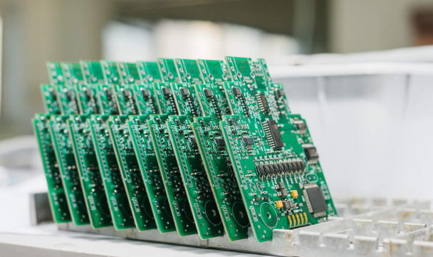
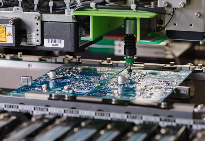
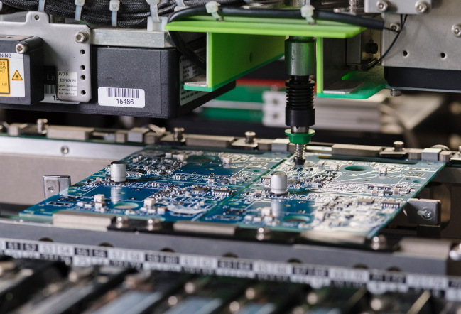
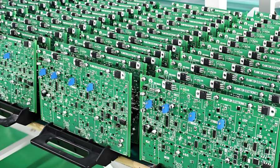
- Mass Production: Stable high‑volume manufacturing with automated production lines, strict process control, and consistent quality for large‑scale market deployment.
- Component Sourcing: Global reliable component supply chain with 100% genuine parts, full traceability, and alternative component support to avoid supply shortages.
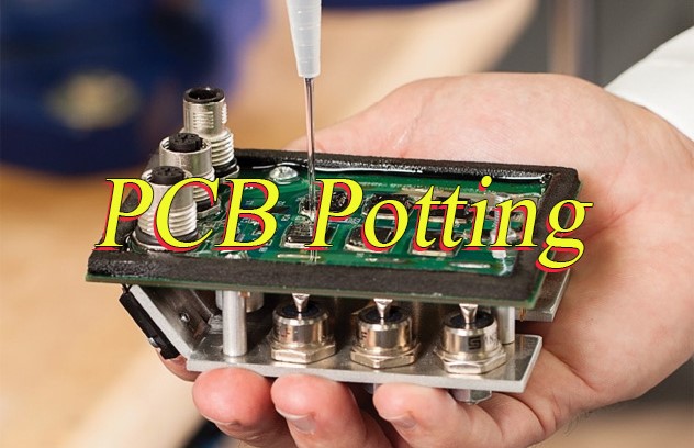
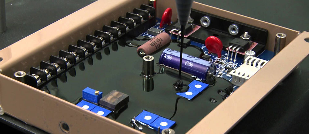
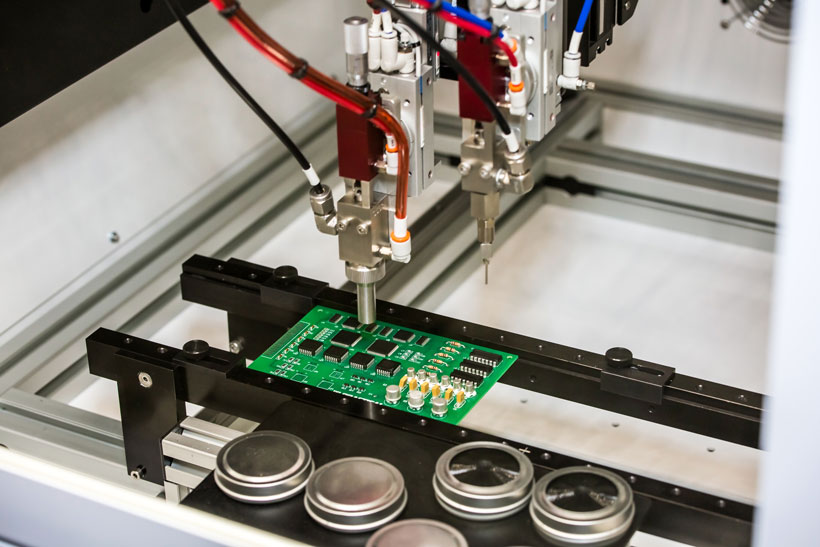
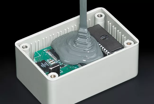
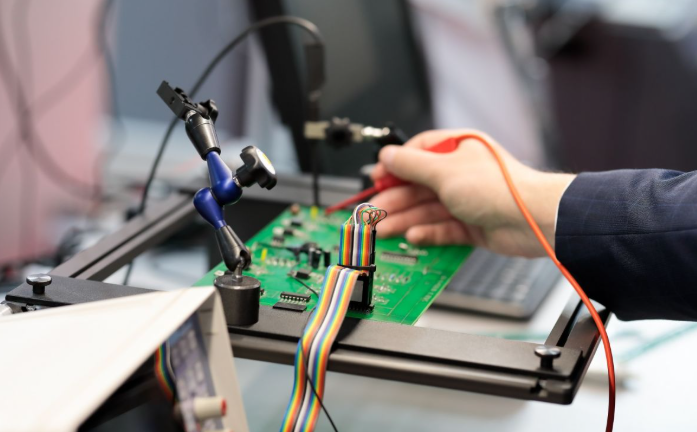
- PCB Assembly: Complete turnkey PCBA services including SMT, DIP, mixed assembly, potting, conformal coating, and functional testing for finished electronic products.
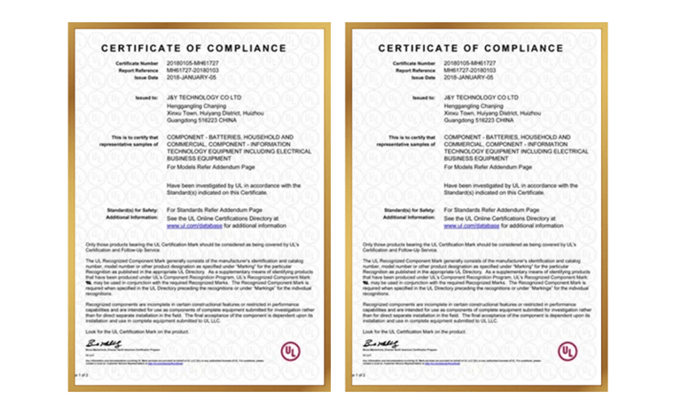
Our Authoritative Quality Certifications for Cambodia PCB Manufacturing Orders
Certifications are not just badges, they are your guarantee of compliance, safety, and reliability. EBest holds industry-leading certifications:
- IATF 16949 – Automotive Electronics Quality Management System
- ISO 9001:2015 – International Quality Management System
- ISO 13485:2016 – Medical Device Quality Management System
- AS9100D – Aerospace Quality Management System
- REACH – EU Chemical Substance Compliance
- RoHS – Hazardous Substance Restriction Compliance
- UL – Safety Certification for Global Market Access
These certifications let you enter global markets with confidence and meet strict customer audit requirements.
PCB Manufacturing Capacity & Advanced Process Capabilities
| Parameter | Detailed Specification |
| Monthly Production Capacity | 260,000 ft² (28,900 m²) |
| Unique Board Types | 1,000+ different board versions |
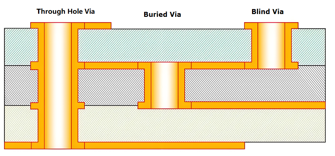
| Layer Count | 1–30 layers |
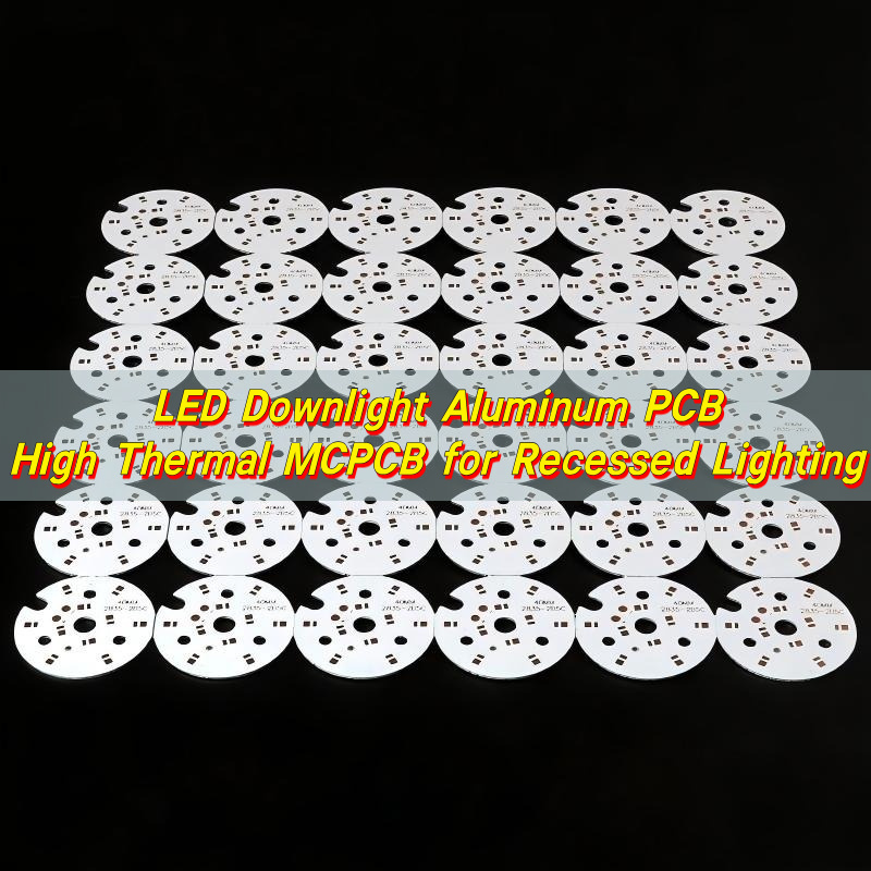
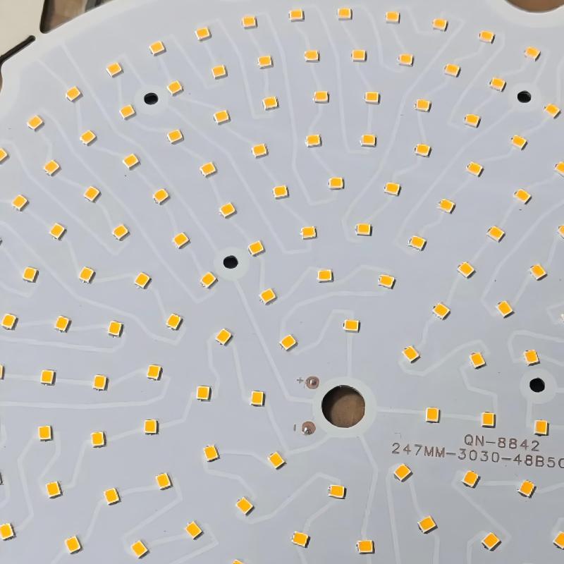
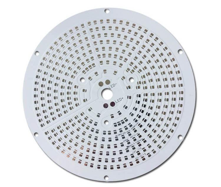
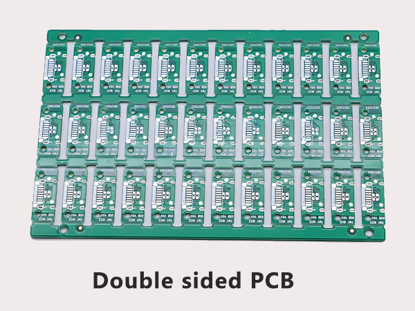
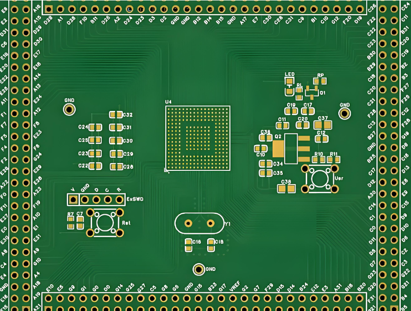
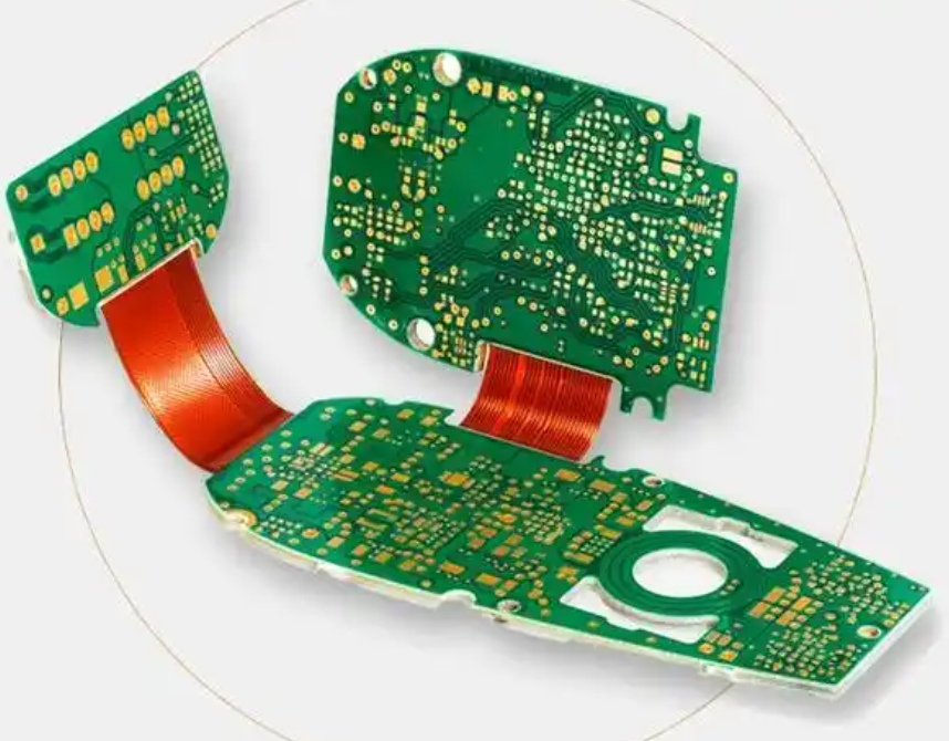
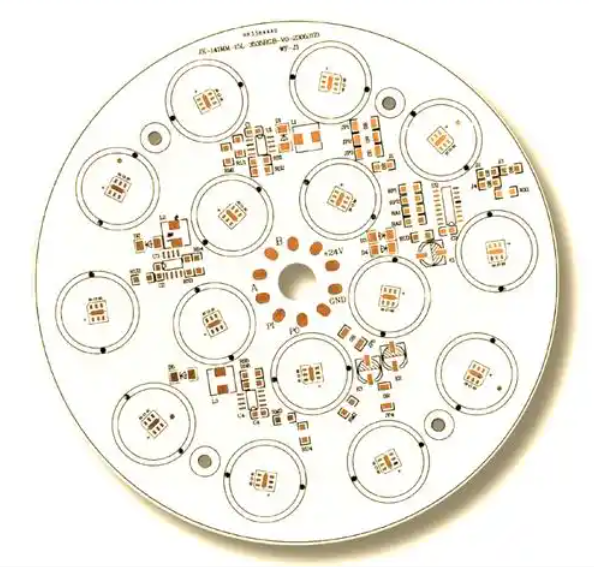
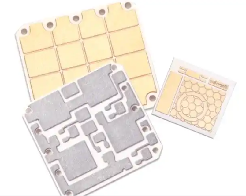
| Base Materials | FR4, Metal Core (MCPCB), Ceramic, Flex, Rigid‑Flex, High Frequency, High TG |
| Minimum Track Width / Space | 3 mil (0.075 mm) |
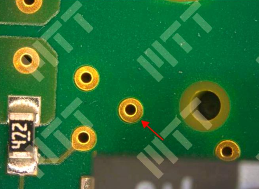
| Minimum Drill Hole Size | 0.15 mm |
| Surface Finishes | HASL, Lead‑Free HASL, ENIG, Immersion Silver, Immersion Tin, OSP |
| Board Thickness Range | 0.2 mm – 6.0 mm |
| Copper Weight | 0.5 oz – 6 oz (Heavy Copper supported) |
| Prototype Lead Time | 24 hours – 5 days |
| Mass Production Lead Time | 7 – 15 days |
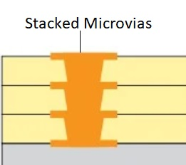
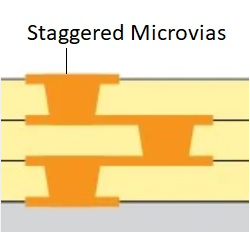
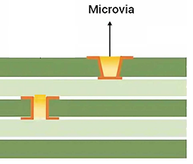
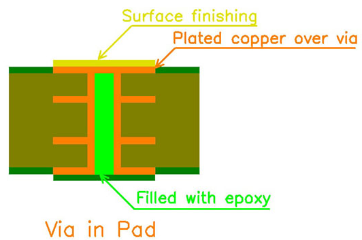
| Special Capabilities | HDI, High‑TG, Impedance Control, High Speed, Heavy Copper, Ultra‑Thin, Busbar, IC Substrate, RF Microwave |
Which Industries in Cambodia Has EBest Served?
EBest provides professional custom PCB and PCB assembly solutions for high‑growth industries that demand strict quality, reliability, and compliance. We focus on four core high‑demand sectors:
Automotive Electronics PCB Solutions
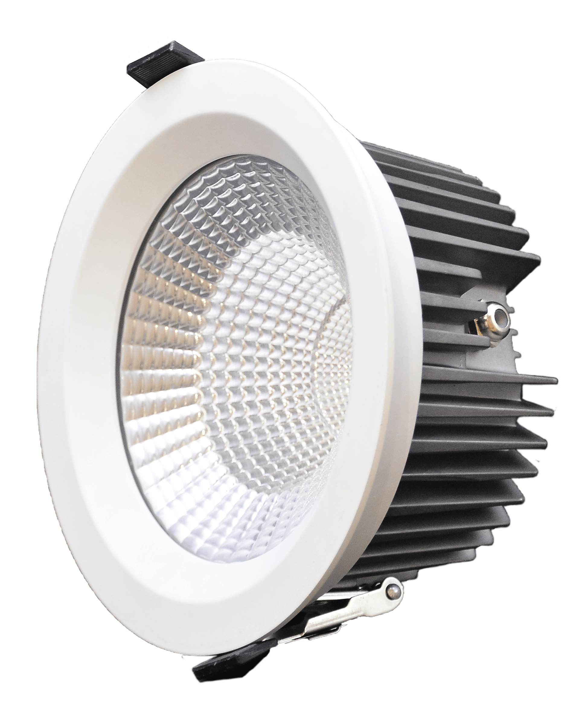
- Applications: Automotive lighting, engine sensors, body control modules, battery management systems (BMS), in‑vehicle infotainment.
- Key Products: Metal Core PCBs, heavy copper PCBs, high‑TG PCBs.
- Advantages: High temperature resistance, vibration resistance, long‑term stability, IATF 16949 certified.
Industrial Control & Automation PCB Solutions
- Applications: PLC controllers, servo drives, industrial sensors, robotics, automation equipment.
- Key Products: Multilayer PCBs, heavy copper PCBs, impedance control PCBs, high‑speed PCBs.
- Advantages: 24/7 stable operation, strong anti‑interference, high reliability for harsh industrial environments.
Medical Electronics PCB Solutions
- Applications: Diagnostic equipment, patient monitors, therapeutic devices, portable medical instruments.
- Key Products: ISO 13485 certified PCBs, ultra‑thin PCBs, HDI PCBs.
- Advantages: High reliability, full material traceability, strict cleanliness, medical regulatory compliance.
Consumer Electronics PCB Solutions
- Applications: Smartphones, wearables, tablets, smart home devices, portable electronics.
- Key Products: HDI PCBs, ultra‑thin PCBs, rigid‑flex PCBs.
- Advantages: High‑density layout, compact size, lightweight, fast prototyping for rapid product development.
How EBest Solves Your Most Critical PCB Sourcing Challenges?
Many engineering and procurement teams face consistent challenges when working with a PCB manufacturer in Cambodia, including delayed deliveries, unstable quality, insufficient certifications, weak technical support, unexpected production failures, and high redesign costs. EBest eliminates these pain points with structured, reliable solutions:
- We deliver predictable, guaranteed lead times so your project stays on schedule.
- Our full inspection system reduces failure rates and minimizes after‑sales issues.
- Complete international certifications ensure full regulatory compliance.
- Free DFM analysis identifies design risks early and lowers total production cost.
- 20+ years of manufacturing experience enables us to handle complex, high‑precision boards.
- Customized manufacturing supports your unique industry, application, and performance needs.
- Integrated one‑stop service reduces supply chain complexity and coordination risk.
When you partner with EBest, you gain long‑term stability, efficiency, and complete peace of mind for every project.
Top 10 PCB Manufacturers in Cambodia in 2026
| Company Name | Certifications | Main Products & Services | Process Capability | Lead Time |
| EBest Circuit | ISO 9001, ISO 13485, IATF 16949, AS9100D, RoHS, UL | FR4, HDI, MCPCB, Ceramic, Flex/Rigid-Flex; Prototype & Mass Production; Full PCB Assembly | 1–30 layers, 0.15 mm min hole, heavy copper, high frequency, impedance control, RF | Prototype: 24h–5d; Mass: 7–15d |
| Cambodian PCB Tech | ISO 9001, RoHS | Single/double-sided, multilayer FR4 PCB; small-batch SMT assembly | 1–8 layers, standard DFM support | Prototype: 5–7d; Mass: 12–20d |
| Mekong PCB Manufacturing | ISO 9001 | Standard rigid PCBs, quick prototypes, basic assembly | 1–6 layers, standard materials | Prototype: 4–6d; Mass: 10–18d |
| SEA Circuit Solutions | ISO 9001, RoHS | Multilayer PCB, LED MCPCB, industrial control boards | 1–12 layers, metal core supported | Prototype: 5–7d; Mass: 12–20d |
| Angkor PCB Assembly | ISO 9001 | PCB fabrication, low-volume assembly, component sourcing | 1–8 layers, basic SMT | Prototype: 5–8d; Mass: 14–22d |
| Phnom Penh PCB Factory | RoHS | Single/double-sided PCB, consumer electronics | 1–4 layers, standard finish | Prototype: 4–6d; Mass: 10–18d |
| Indochina PCB Co., Ltd. | ISO 9001 | Multilayer PCB, prototype service, quick turnaround | 1–10 layers, standard DFM | Prototype: 4–7d; Mass: 12–20d |
| Royal PCB Manufacturing | ISO 9001, RoHS | FR4 PCB, MCPCB for lighting | 1–8 layers, thermal management | Prototype: 5–7d; Mass: 12–20d |
| Golden PCB Cambodia | RoHS | Basic rigid PCB, consumer electronics, small batch | 1–4 layers, standard materials | Prototype: 5–8d; Mass: 14–22d |
| Advance PCB Tech | ISO 9001 | High-TG PCB, heavy copper, industrial & automotive | 1–12 layers, high temperature resistant | Prototype: 5–7d; Mass: 12–20d |
How to Select a Reliable PCB Manufacturer in Cambodia?
Choosing a reliable PCB manufacturer in Cambodia is critical for product quality and supply chain security. Use these professional, practical criteria to evaluate partners:
- Verify complete, valid, and industry‑matched certifications (ISO 9001, IATF 16949, ISO 13485, AS9100D, UL, RoHS).
- Confirm real process capabilities, including layer count, minimum hole size, impedance control, HDI, high frequency, and heavy copper.
- Evaluate actual on‑time delivery performance, not just advertised lead time.
- Check professional technical support, especially free DFM analysis and custom design capabilities.
- Review full quality control systems and testing procedures.
- Assess production scale, equipment level, and ability to support both prototypes and mass production.
- Confirm one‑stop service capability to reduce supply chain complexity.
EBest meets and exceeds all these standards, making us the most trusted choice for global buyers.
How Fast Can I Get PCB Prototypes & Mass Production in Cambodia?
Lead time directly affects your R&D progress and market launch. As a leading PCB manufacturer in Cambodia, EBest maintains industry‑leading turnaround while upholding strict quality standards.
- Standard PCB Prototype: 3–5 days.
- Expedited Emergency Prototype: 24 hours.
- Standard Multilayer Mass Production: 7–15 days.
- Complex HDI / High‑Frequency / Rigid‑Flex: 10–20 days.
We balance speed, quality, and reliability to support your most aggressive project schedules.
FAQs About PCB Manufacturer in Cambodia
Q1: Do you provide free DFM analysis for PCB designs?
A1: Yes, EBest offers free DFM reports to optimize your design, avoid production risks, improve yield, and reduce manufacturing costs.
Q2: Can you support fully custom PCB manufacturing?
A2: Yes, we provide full custom PCB solutions including layer count, base material, surface finish, impedance control, HDI, high frequency, heavy copper, and rigid‑flex designs.
Q3: What international certifications do you hold?
A3: We hold IATF 16949, ISO 9001:2015, ISO 13485:2016, AS9100D, REACH, RoHS, and UL certifications.
Q4: What is your minimum order quantity (MOQ) for prototypes?
A4: We support low MOQ for prototype projects to accommodate R&D, testing, and startup development.
Q5: How fast is your expedited PCB prototype service?
A5: Our emergency expedited service supports shipping within 24 hours for urgent and critical projects.
Q6: Do you offer full turnkey PCB assembly (PCBA) services?
A6: Yes, we provide one‑stop PCB assembly including component sourcing, SMT, DIP, mixed assembly, conformal coating, and functional testing.
Q7: Can you produce high‑frequency, HDI, and heavy copper PCBs?
A7: Yes, we specialize in advanced PCB types including high‑frequency, HDI, heavy copper, rigid‑flex, high‑TG, and impedance‑controlled boards.
Q8: Is full material traceability available for medical and automotive projects?
A8: Yes, full material traceability is standard for medical, automotive, aerospace, and other high‑reliability applications.