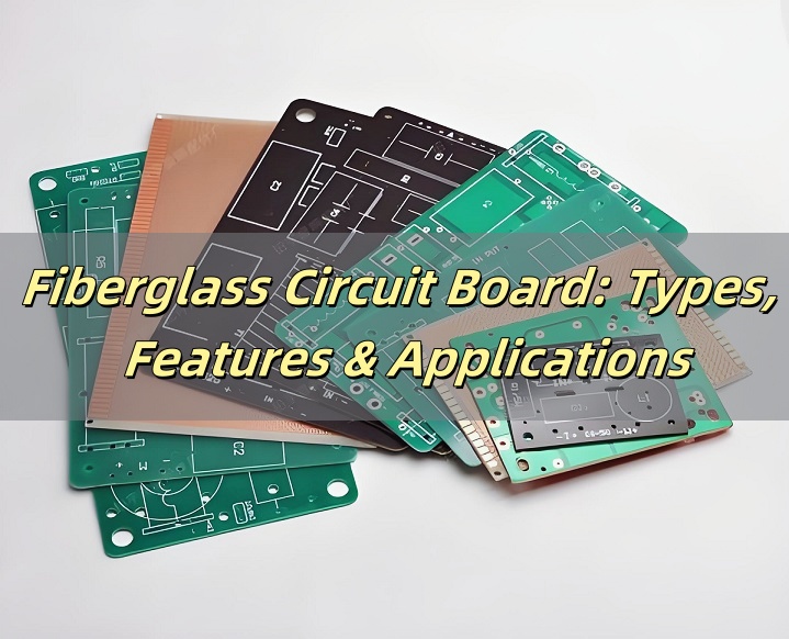
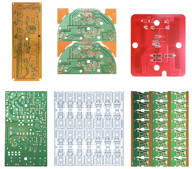
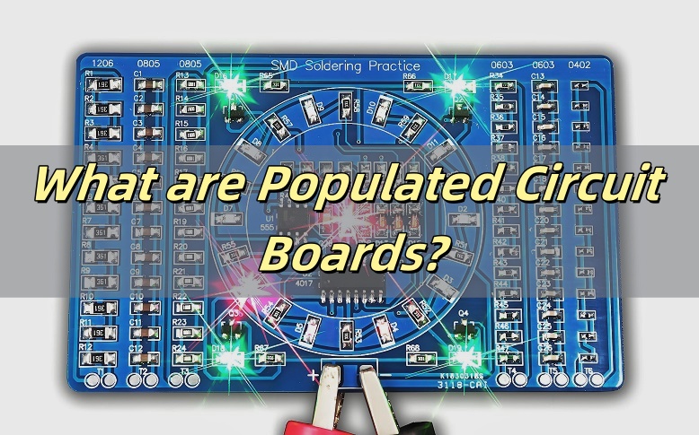
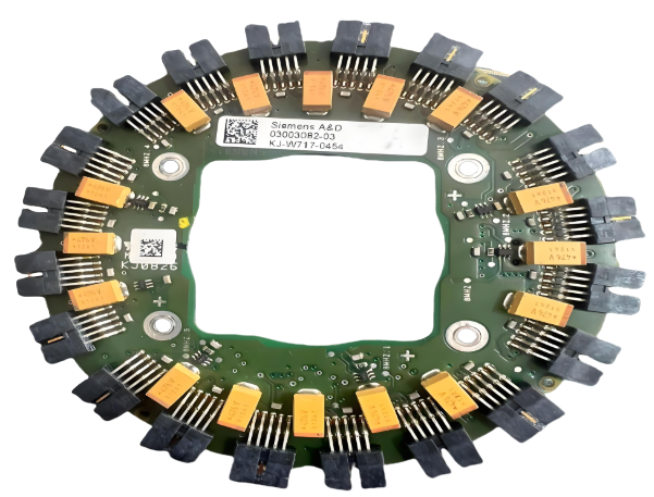
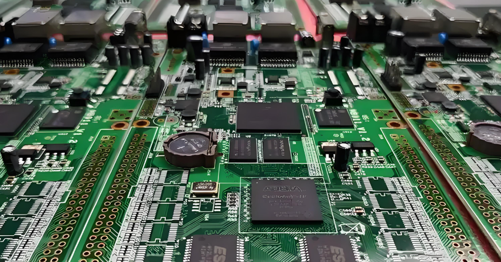
In the electronics world, one term you’ll often hear is populated circuit boards. These are circuit boards that have all the needed electronic parts added to them, such as chips, resistors, capacitors, and connectors. Populated PCBs are the heart of almost every electronic device we use today—from smartphones and TVs to medical tools and industrial machines.
At EBest Circuit (Best Technology), we specialize in populated PCB assembly services for clients across the globe. With over 18 years of experience, we are a leading PCB assembly manufacturer based in China and Vietnam. We provide turnkey PCB assembly, SMT assembly, and through-hole component soldering. Whether you need low-volume prototypes or mass production, our team ensures every PCB with components is built to the highest quality standards. This blog will help you better understand what populated PCBs are, how they’re made, and why choosing the right manufacturer like EBest Circuit (Best Technology) matters.
What Is a Populated Circuit Board?
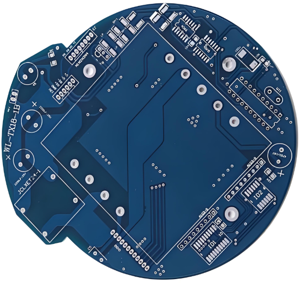
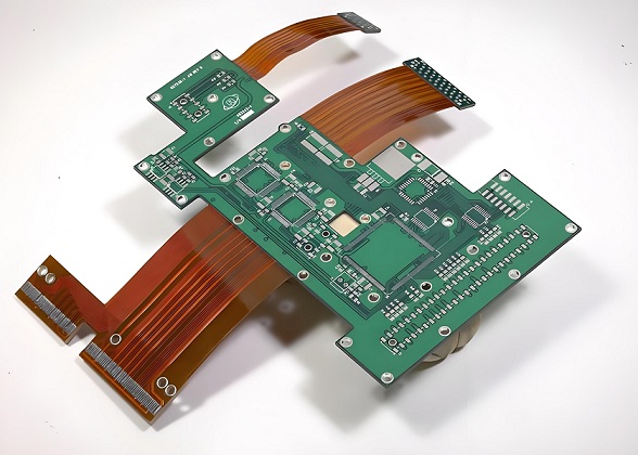
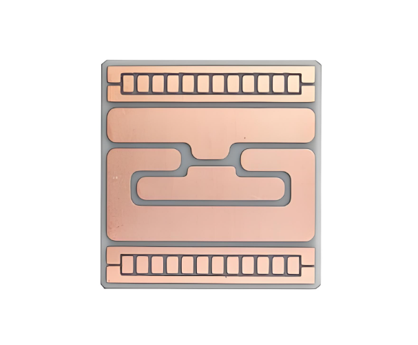
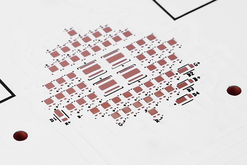
A populated circuit board means a PCB that already has all its electronic parts placed and soldered onto it. These parts are selected based on the board’s design and function. The term “populated” means that the bare board is now filled with parts and ready to perform tasks in a larger system.
Before population, the board is just a base with copper traces—it’s called a bare PCB or blank PCB. After adding components like ICs, capacitors, and connectors, it becomes a populated PCB, also called PCBA (assembled PCB). This fully assembled board can now be installed in devices like computers, smart watches, control panels, and more.
What Does Populate Mean in Electronics?
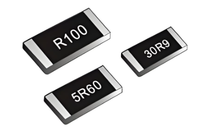
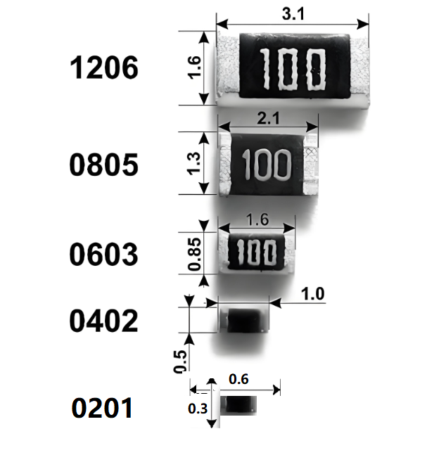
In the electronics industry, the word “populate” means to place/mount parts onto a PCB. These parts include both surface mount devices (SMDs) like leds, resistors, capacitors, chips and through-hole components like connectors. The process of placing and soldering these components is called PCB population or PCB assembly.
There are two main methods:
- SMT (Surface Mount Technology): Parts are placed on the surface of the board and soldered using reflow ovens.
- THT (Through-Hole Technology): Leads of components go through holes and are soldered on the other side.
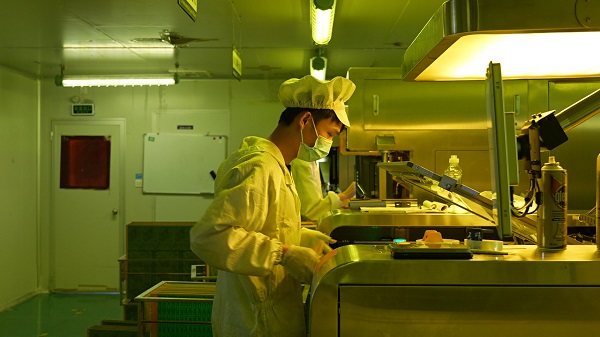
PCB population can be done manually in small runs or by automated machines for larger batches. At EBest Circuit (Best Technology), we have 10+ automated pick and place machine to improve the whole populated efficiency.
What Is the Difference Between a Bare PCB and a Populated PCB?
| Feature | Bare PCB | Populated PCB |
| Component Status | No components | Fully assembled with components |
| Functionality | Not functional | Fully functional |
| Manufacturing Stage | Early stage | Final assembly |
| Application | Not used directly in devices | Installed in end-use products |
A bare PCB is like the foundation base of network. It contains copper tracks and pads that show where components will go. But it can’t do anything on its own. A populated circuit board is the completed product, which can be directly integrated into your electronic devices and function by power on.
How Are Circuit Boards Populated?
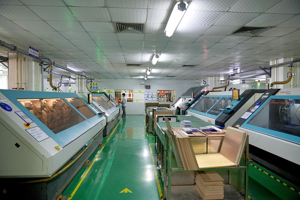
The PCB population process is PCB assembly process, it includes several precise steps. At EBest Circuit (Best Technology), we use advanced pick and place machines and IPC-certified processes to ensure every board meets your specs.
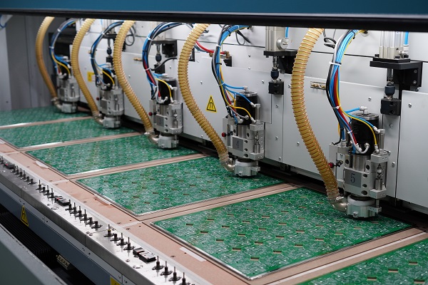
1. Solder Paste Printing
The PCB population process started on solder paste printing. A stencil is used to apply solder paste onto the pads of the PCB evenly and then inspect by SPI machine. This paste will later hold the surface mount components in place during reflow soldering.
2. Component Placement
Pick-and-place machines accurately place each SMD component on the paste-covered pads. This step must be done quickly and precisely, so an experienced and full-skilled operator is necessary.
3. Reflow Soldering
The board passes through a reflow oven. The solder paste melts and solidifies, bonding each part to the board. SMT assembly is now complete.
4. Through-Hole Assembly (if needed)
Larger parts like connectors, transformers, or buttons may need through-hole soldering, done either manually or using wave soldering.
5. Inspection and Testing
We inspect the populated circuit boards using AOI (Automated Optical Inspection), X-ray inspection, and functional testing to ensure quality.
6. Cleaning and Packing
Residue from soldering is cleaned, and the boards are packaged to prevent damage during shipping.
At EBest Circuit (Best Technology), each step is handled by skilled engineers and operators to ensure a smooth populated PCB assembly process.
4 Tips for a Successful PCB Population Process
1. Start With a DFM-Checked Design
Design for Manufacturability (DFM) is the first checkpoint. Before you send your PCB files to a manufacturer, check if the board can be assembled easily and correctly. Or choose a PCB manufacturer who provide DFM or DFA service.
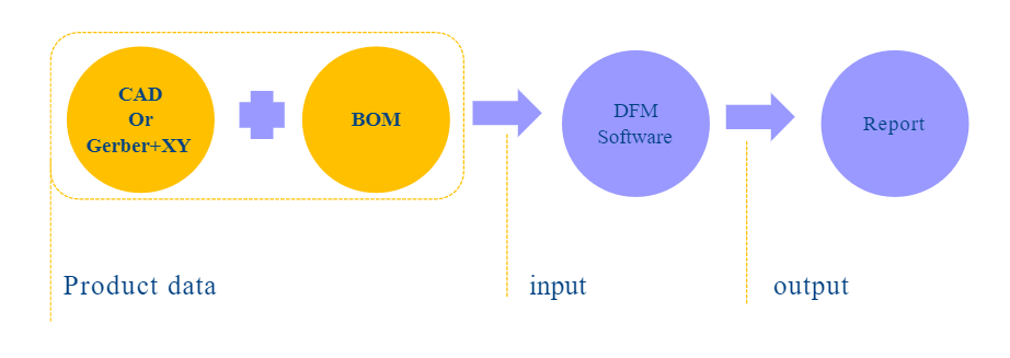
2. Use a Clear and Updated BOM
The Bill of Materials (BOM) should list every component—clearly and accurately. Include part numbers, descriptions, footprints, and preferred brands. A clear BOM can save much time during the assembly process.
3. Consider Thermal Profiles for Reflow
For SMT assembly, different components may require different heat levels during reflow soldering. Make sure to plan a proper thermal profile so that the solder melts without damaging parts. This is especially important for BGA and QFN packages.
4. Work With an Experienced Manufacturer
Choose a partner like EBest Circuit (Best Technology) that offers end-to-end PCB services. Experience means fewer errors, smoother communication, and faster lead times. We’ve been handling populated PCB assembly since 2006, delivering consistent quality and reliability.
Factors That Affect Populated Circuit Boards Price
When estimating the cost of a populated PCB, many buyers think it’s just about part prices and labor. But there are many hidden and visible factors that influence the final price of PCB assembly. As an 18+ years experienced PCBA manufacturer, let me explain what affects the cost:
1. Board Complexity and Size
The more layers your PCB has, the more it costs to manufacture and assemble. Also, large boards use more material and take more time to populate. HDI boards or boards with fine-pitch components also increase cost.
2. Type and Quantity of Components
Boards with hundreds of parts will naturally cost more to assemble than simple ones. Expensive components like processors or specialized sensors also add to the cost.
3. Assembly Technology Used
SMT assembly is faster and cheaper for high volumes. But if your board includes many through-hole components, it may require manual soldering or wave soldering, which takes more time and labor.
4. Sourcing Strategy
You can either supply your own components (consigned assembly) or let the manufacturer handle it (turnkey assembly). While turnkey PCB assembly is convenient, the cost will include sourcing, logistics, and possible part markups.
5. Testing Requirements
Some applications require basic functional testing, while others need ICT (In-Circuit Testing) or burn-in tests. These tests improve product quality but also add to the price of the populated PCB.
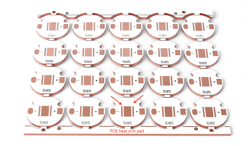
6. Packaging and Handling
If your board includes sensitive parts like BGAs or LEDs or irregular components, which need to customize package, this may add extra cost slightly.
7. Order Volume and Lead Time
Larger orders usually come with volume discounts. However, rush orders or quick-turn PCB assemblies may cost more due to overtime labor, expedited shipping, and quick part sourcing.
8. Quality Standards
If your board needs to meet IPC Class 3, the price may be higher. Certified lines have tighter controls and may use higher-quality materials. At EBest Circuit (Best Technology), IPC class 2 is the default standard, customers should point out if they want to follow class 3.
9. NRE (Non-Recurring Engineering) Fee
Don’t doubt, the NRE fee is a one-time setup cost charged at the start of a new project. It covers things like:
- Tooling for solder stencils
- First-article inspection
- Programming of pick-and-place machines
This cost isn’t charged again for repeat orders, but it’s important to include it in your project quote. At EBest Circuit (Best Technology), we keep NRE fees transparent and as low as possible—especially for long-term clients or volume repeat orders.
What Is the HS Code for Populated PCBs?
When shipping populated PCBs internationally, you’ll need to use a proper HS Code. The commonly used code for populated circuit boards is: 853400
This code is used for printed circuit card assemblies (PCAs) and fully assembled electronic boards. Depending on the country, sub-codes may apply based on the board’s use (e.g., medical vs. telecom). For smooth customs clearance, always consult your freight agent or your local logistic company like FedEx, DHL or UPS.
What Are the Applications of Populated Circuit Boards?
- Consumer Electronics: Smartphones, laptops, smart speakers, and gaming consoles.
- Medical Devices: Monitoring systems, diagnostic machines, and handheld tools.
- Automotive Systems: Car control units, infotainment panels, and ADAS systems.
- Industrial Automation: PLCs, motor controllers, sensors, and robotics.
- Aerospace and Defense: Flight control, radar systems, and communication tools.
- Telecommunication: Routers, base stations, and 5G network boards.
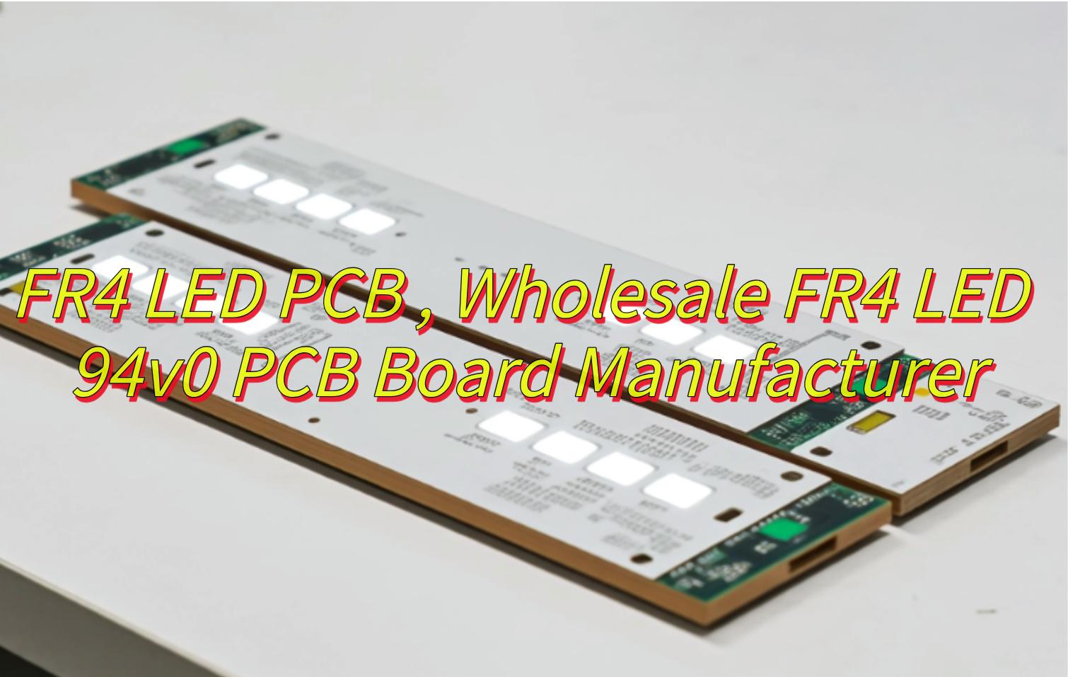
- LED Lighting Systems: Driver boards, dimmers, and smart lighting controls.
- No matter the industry, a reliable PCB assembly manufacturer is crucial for success.
Why Choose EBest Circuit (Best Technology) for Your Populated Circuit Boards?
At EBest Circuit (Best Technology), we’ve been helping companies worldwide since 2006 with high-quality PCB assembly services. Here’s why our clients choose us:
✅ One-Stop Service: From bare PCBs to full turnkey PCB assembly.
✅ Rich Experience: Over 18 years serving over 1200+ clients.
✅ High-Precision Equipment: SMT lines, AOI, X-ray, ICT, and functional testing.
✅ Custom Solutions: We build prototypes and mass production, both fast and cost-effective.
✅ Global Delivery: We ship populated PCBs to over 60 countries.
✅ Certifications: ISO9001, ISO13485, RoHS, and IPC-A-610 standards.
Our team works closely with you to understand your project goals, timelines, and quality expectations. Whether you need a populated PCB prototype or high-volume orders, EBest Circuit (Best Technology) delivers with speed, accuracy, and care.
FAQs
1. Can I reuse components from a populated PCB?
Yes, with care. Desoldering is possible, but components may degrade with heat exposure. It’s viable for prototyping but not for production.
2. What’s the typical lead time for manufacturing?
Depending on complexity, anywhere from 3 days for prototypes to several weeks for complex assemblies.
3. Can I provide my own components for PCB population?
Yes, of course. This is called consigned assembly. If you already have the components, you can send them to your PCB assembler. At EBest Circuit (Best Technology), we support both consigned and turnkey services, giving you full flexibility.
4. What files are needed to start PCB population?
To start your PCB population project, you’ll need to provide:
- Gerber files
- Bill of Materials (BOM)
- Pick-and-place file (Centroid)
- Assembly drawing or 3D file (optional but helpful)
If you’re not sure how to prepare these files, EBest Circuit (Best Technology)’s engineering team can guide you through the process.
5. How do you ensure the quality of populated circuit boards?
At EBest Circuit (Best Technology), quality is our top priority. We use:
- AOI (Automated Optical Inspection)
- X-ray inspection for BGAs and multilayers
- In-circuit testing (ICT)
- Functional testing based on your requirements
Every populated PCB is checked before shipment to make sure it works perfectly in your product.