Daughter board is a term you might hear often when dealing with modular or expandable electronics. Whether you’re working on an industrial control system or building a custom computing platform, daughter boards play an essential role in modern circuit design. They provide a flexible way to add functions without reworking the main PCB. In this blog, we’ll explain what a daughter board is, how it compares to a motherboard, where it’s used, and how you can design or source one with support from EBest Circuit (Best Technology).
What Is a Daughter Board?
A daughter board is a secondary printed circuit board (PCB) that connects to a larger mainboard or motherboard to expand the system’s functions. Think of it as an add-on card or module. It doesn’t work alone but works in combination with a central PCB. It often contains components such as integrated circuits, connectors, sensors, or specialized chips.
These boards are commonly used when the system needs modular features, like upgrading ports, adding wireless capabilities, or supporting additional I/O. For example, in a test system, you might use one daughter board for analog inputs and another for digital outputs.
What Is Another Name for a Daughter Board?
Daughter boards are known by different names depending on their role or industry. Some common synonyms include:
- Daughter card
- Mezzanine board
- Add-on board
- Expansion board
- Piggyback board
All these terms describe the same core idea—a smaller board that connects to and works with a larger one.
Types of Daughter Boards
Daughter boards come in many forms, each built to serve a particular function. They help expand the capabilities of the mainboard while keeping the system modular and easier to maintain. Here are the most common types used in computing, electronics, and industrial applications:
1. RAM DIMMs (Dual Inline Memory Modules)
RAM DIMMs are one of the most recognized daughter boards used in computers. These modules plug directly into designated memory slots on the motherboard. Their job is to increase a system’s memory capacity, allowing it to handle more data and run applications smoothly.
In modern computing, larger RAM is essential for multitasking, video editing, gaming, and server operations. DIMMs come in different sizes and speeds—such as DDR4 and DDR5—and are easily replaceable. Without them, most systems would be stuck with limited onboard memory, which slows down performance.
2. Storage Expansion Boards
Storage expansion boards provide extra connections for drives like HDDs (Hard Disk Drives) or SSDs (Solid-State Drives). These daughter boards offer additional interfaces such as SATA, NVMe, U.2, or M.2 that might not be available on the motherboard.
Some advanced boards also include built-in RAID support, which protects data by mirroring or distributing it across multiple drives. These are especially useful in servers, data centers, and high-performance computing where fast and reliable storage is a top priority.
3. Graphics Cards (GPUs)
Graphics cards are powerful daughter boards that handle video output and image rendering. They connect through slots like PCIe and often come with their own processors, memory, and cooling systems. This makes them ideal for graphic-intensive applications such as gaming, animation, 3D rendering, and AI computations.
A dedicated GPU offloads tasks from the CPU, significantly improving performance in systems that need to display complex visuals. While some basic systems use integrated graphics, most high-performance setups depend on discrete GPU daughter boards.
4. Network Interface Cards (NICs)
Network Interface Cards are daughter boards that enable wired or wireless network connectivity. While many modern motherboards come with built-in Ethernet or Wi-Fi, NICs are still widely used for upgrading to higher-speed interfaces (such as 10GbE) or adding more ports.
These boards are commonly found in servers, workstations, and gaming systems. In industrial applications, NICs may support fiber optics, PoE (Power over Ethernet), or advanced features like VLAN tagging and network booting.
5. Audio Processing Boards
Audio daughter boards process sound input and output. Unlike basic onboard audio systems, these specialized boards use high-quality digital-to-analog converters (DACs), pre-amplifiers, and noise filters to deliver clearer, richer audio.
They are widely used in music production, live broadcasting, home theater setups, and gaming rigs. Some also support surround sound formats and professional studio interfaces. If audio quality is critical to your application, a dedicated audio processing board is a valuable upgrade.
6. Display Interface Boards
Display interface boards handle video signal conversion and output for external screens. These daughter boards may include HDMI, VGA, DVI, DisplayPort, or LVDS connectors. In embedded systems, you may also find boards designed to interface directly with LCD or OLED panels.
They are commonly used in digital signage, kiosks, medical imaging devices, and control panels where display requirements vary. By offloading display functions to a daughter board, designers can support multiple screen types without changing the mainboard.
7. Power Regulation Boards
Power regulation boards manage how power is distributed and controlled in an electronic system. They often perform tasks such as voltage step-down/up, current limiting, charging, or power sequencing. These daughter boards are important in devices that require multiple voltage rails or battery management.
In portable devices, these boards ensure efficient use of power while protecting sensitive circuits. In larger systems, they may provide isolation between different zones or convert AC to DC. By moving these functions off the mainboard, designers save space and improve thermal performance.
8. Customization Boards
Customization boards, also known as breakout boards or feature boards, are developed for specific functions that aren’t supported by standard modules. These may include:
- Touchscreens and user interface buttons
- Sensor modules for temperature, humidity, gas, or motion
- GPS, GSM, or LoRa communication modules
- Data acquisition boards for test systems
Engineers often design these boards for quick testing, prototyping, or low-volume applications where flexibility is key. They offer a fast and affordable way to add new features without redesigning the whole system.
What Is the Function of a Daughter Board?
The primary function of a daughter board is to provide additional features or functionality to a mainboard. Here are some specific functions it can serve:
- Add new sensors or interfaces
- Upgrade or replace audio/video output
- Provide motion or location tracking
- Manage specific voltage domains
- Extend computing power with co-processors
- Act as a debugging or testing interface
Instead of placing all features on one large board, designers break them up into smaller, modular boards. This approach saves space, simplifies design updates, and reduces cost for future upgrades.
What Is the Difference Between a Motherboard and a Daughterboard?
The motherboard is the main printed circuit board (PCB) in a device. It acts as the central hub that connects all critical components—such as the CPU, memory, storage, power supply, and input/output interfaces. It handles communication between all subsystems and manages the overall operation of the device.
In contrast, a daughterboard is a secondary PCB that connects to the motherboard to add or enhance a specific function. It cannot work independently. Instead, it extends the capabilities of the mainboard by providing extra features like sound processing, network connectivity, graphics acceleration, or additional input/output ports. Here’s a simple comparison:
| Feature | Motherboard | Daughter Board |
| Role | Core system board | Add-on module |
| Size | Larger | Smaller |
| Function | Main processor and system logic | Extended features |
| Upgrade | Rarely replaced | Easily replaced or upgraded |
| Examples | PC mainboard, controller board | Audio module, sensor board, NIC |
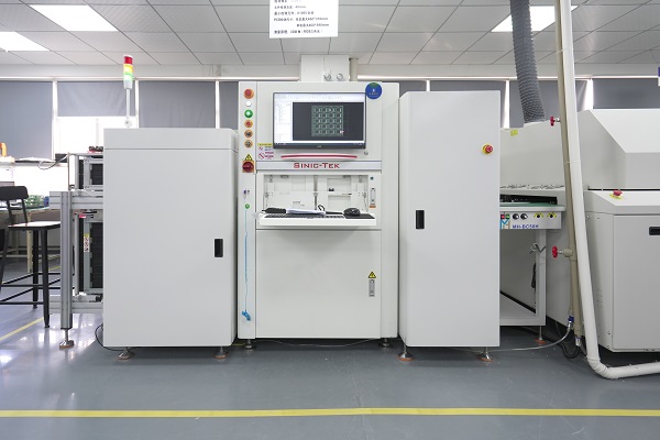
At EBest Circuit (Best Technology), we support both motherboard and daughterboard PCB fabrication. Our team can help you plan, prototype, and produce modular solutions with optimal connector design, layout suggestions, and fast production turnaround.
Daughter Board Price
The cost of a daughter board depends on its design, complexity, and production quantity. Here’s a general pricing guide:
- Basic I/O boards (2-layer, few components): $5–$15 each in volume.
- Sensor modules or wireless boards: $15–$40 depending on components.
- Multilayer signal boards (4–6 layers): $50–$100+ per board.
- Prototyping runs (low volume): Higher due to tooling, setup, and test costs.
Factors that affect price:
- Board size and layer count
- Type of connectors
- Components used (standard vs. custom)
- Surface finish and solder mask
- Quantity ordered
If you’re looking for a cost-effective daughter board PCB, EBest Circuit (Best Technology) can offer you accurate quotes with options to fit your budget.
What Is a Daughter Board Used For?
Daughter boards are used across different industries where customization or modularity is a priority:
1. Industrial automation like sensors, control relays, and communicate with programmable logic controllers (PLCs).
2. Bluetooth or Wi-Fi modules in speakers, smart appliances, and gadgets are often built as daughter boards.
3. Automotive’s ECUs to handle GPS, entertainment, camera feeds, or battery management.
4. In medical devices like portable monitors or scanners, daughter boards add ECG, pulse oximetry, or USB functionality.
5. Aerospace and military, used in systems where functions are split across ruggedized modules for reliability and repair.
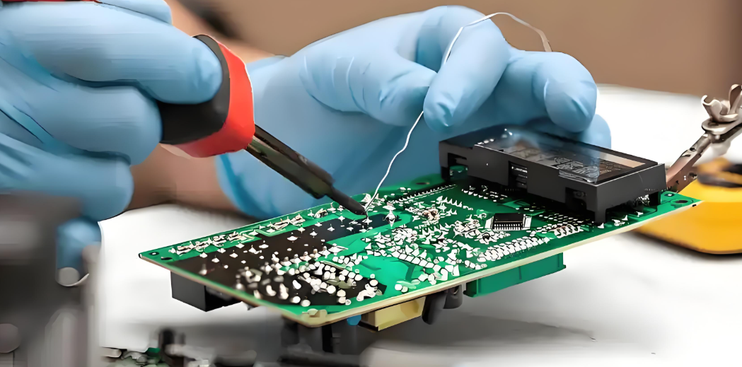
How to Install a Daughter Board?
Installing a daughter board is usually simple, but care is required. Follow these steps:
1. Turn off the system power and discharge static from your body by touching a grounded metal surface.
2. Check the orientation of the daughter board. Make sure the connector lines up properly.
3. Press the board gently into the socket or header on the motherboard. Do not force it.
4. Secure it with screws or stand-offs if needed.
5. Turn on the power and check the function through your interface or software.
Use the correct tools and avoid touching exposed pins. Improper installation could cause short circuits or connector damage.
Daughter Board Design Tips
Designing a daughter board may seem straightforward, but it requires careful planning to ensure it connects well with the motherboard, functions reliably, and remains easy to manufacture. Whether you’re building a sensor module, a power board, or a display interface, good design practices can help you avoid problems later in production and testing. Here are some essential design tips to keep in mind:
1. Choose the Right Connector
The connection between the daughter board and motherboard is the most critical part of your design. You’ll need to pick the correct board-to-board connector or interface based on your application.
Consider:
- Pin count
- Current rating
- Pitch and alignment
- Mounting method
Use high-quality connectors that are easy to assemble and can tolerate vibration or movement if your system is in a harsh environment.
2. Plan for Mechanical Fit and Mounting
Your daughter board should physically fit into the product enclosure or case. Make sure to:
Define the exact outline dimensions and height of the board.
- Avoid component collisions between the daughter board and nearby parts.
- Use stand-offs, screws, or plastic clips to secure the board and reduce strain on the connectors.
- Align connectors precisely to prevent stress or misalignment during insertion.
A good 3D model of your enclosure and PCB assembly helps catch these issues early.
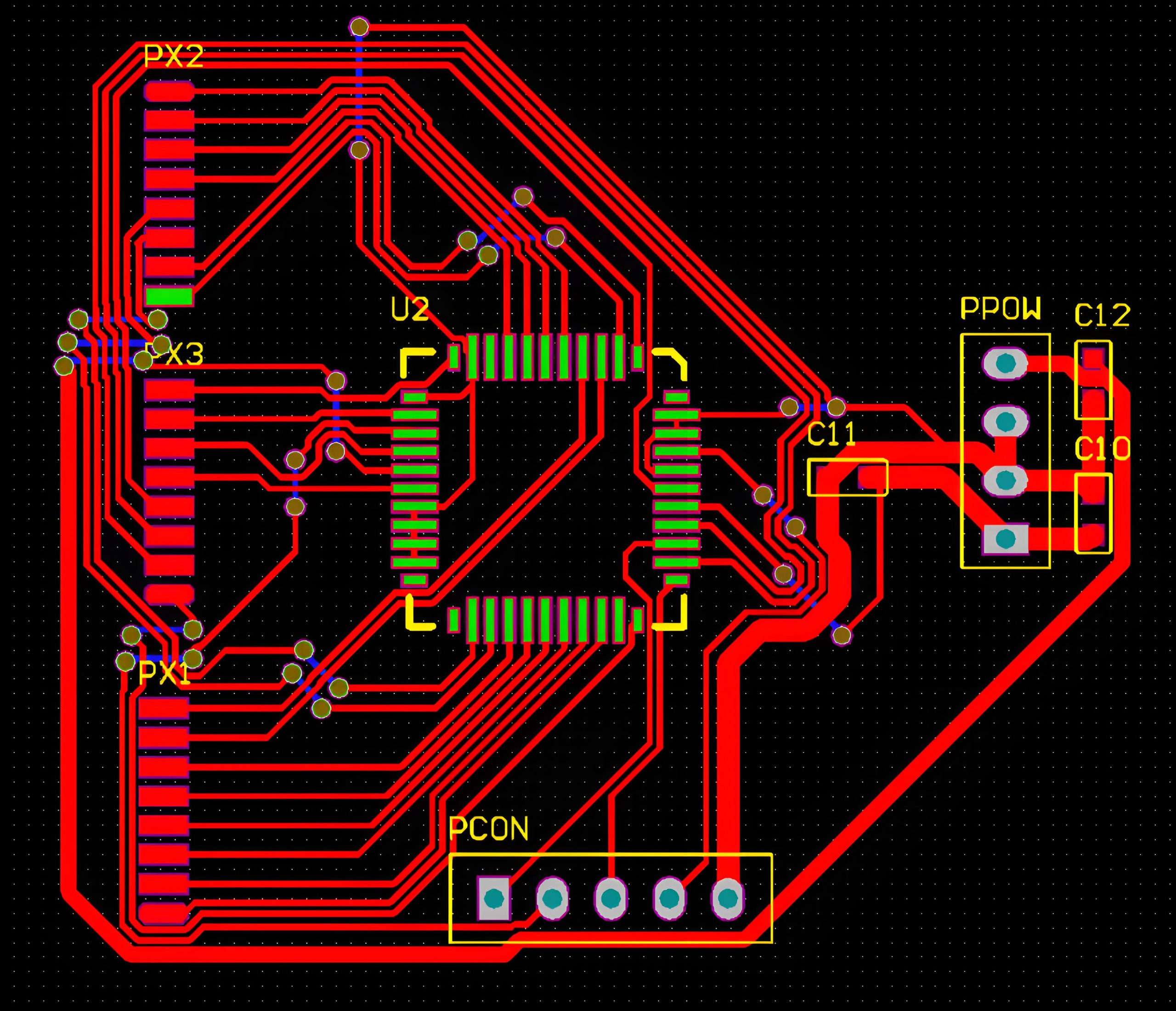
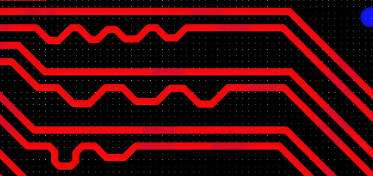
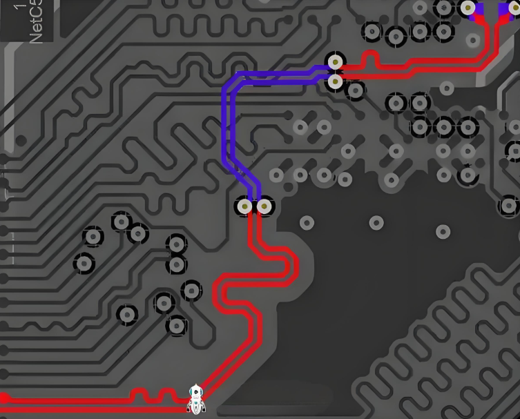
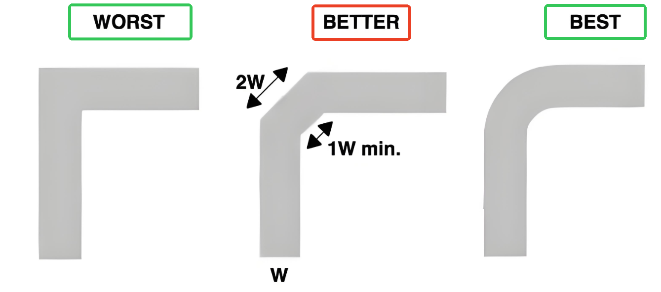
3. Optimize Signal Routing
Careful trace routing ensures signal integrity, especially for high-speed interfaces. Some tips include:
- Short and direct traces between the connector and active components.
- Controlled impedance routing for high-speed or differential signals (USB, HDMI, LVDS, etc.).
- Keep analog and digital signals separated to reduce interference.
- Route ground and power planes to provide a stable return path.
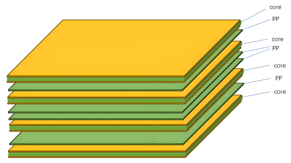
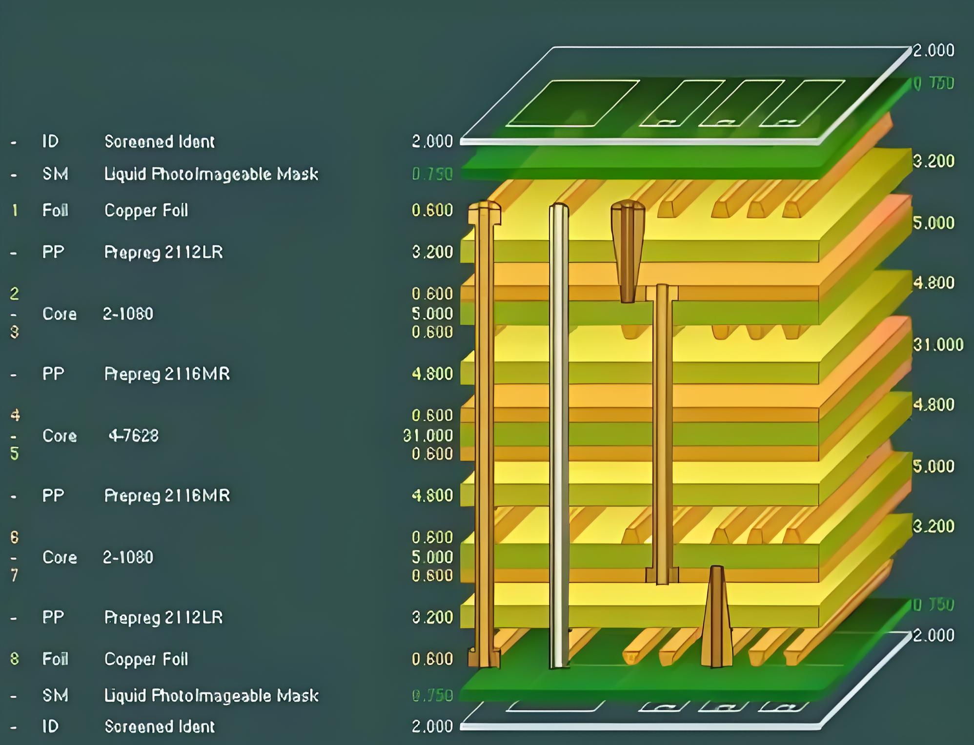
For multi-layer daughter boards, a 4-layer stackup (signal–ground–power–signal) is a good starting point for balanced routing.
4. Manage Power Distribution Carefully
The daughter board may receive power from the motherboard or have its own power input. In either case, power management is crucial:
- Use fuses or protection diodes to prevent reverse polarity and short circuits.
- Include decoupling capacitors near every IC to filter noise.
- Ensure power and ground lines are thick enough to carry the required current.
- If different voltage levels are used (e.g., 5V and 3.3V), use voltage regulators or level shifters.
Clear power planning prevents issues like overheating, unstable voltage, or damage to connected boards.
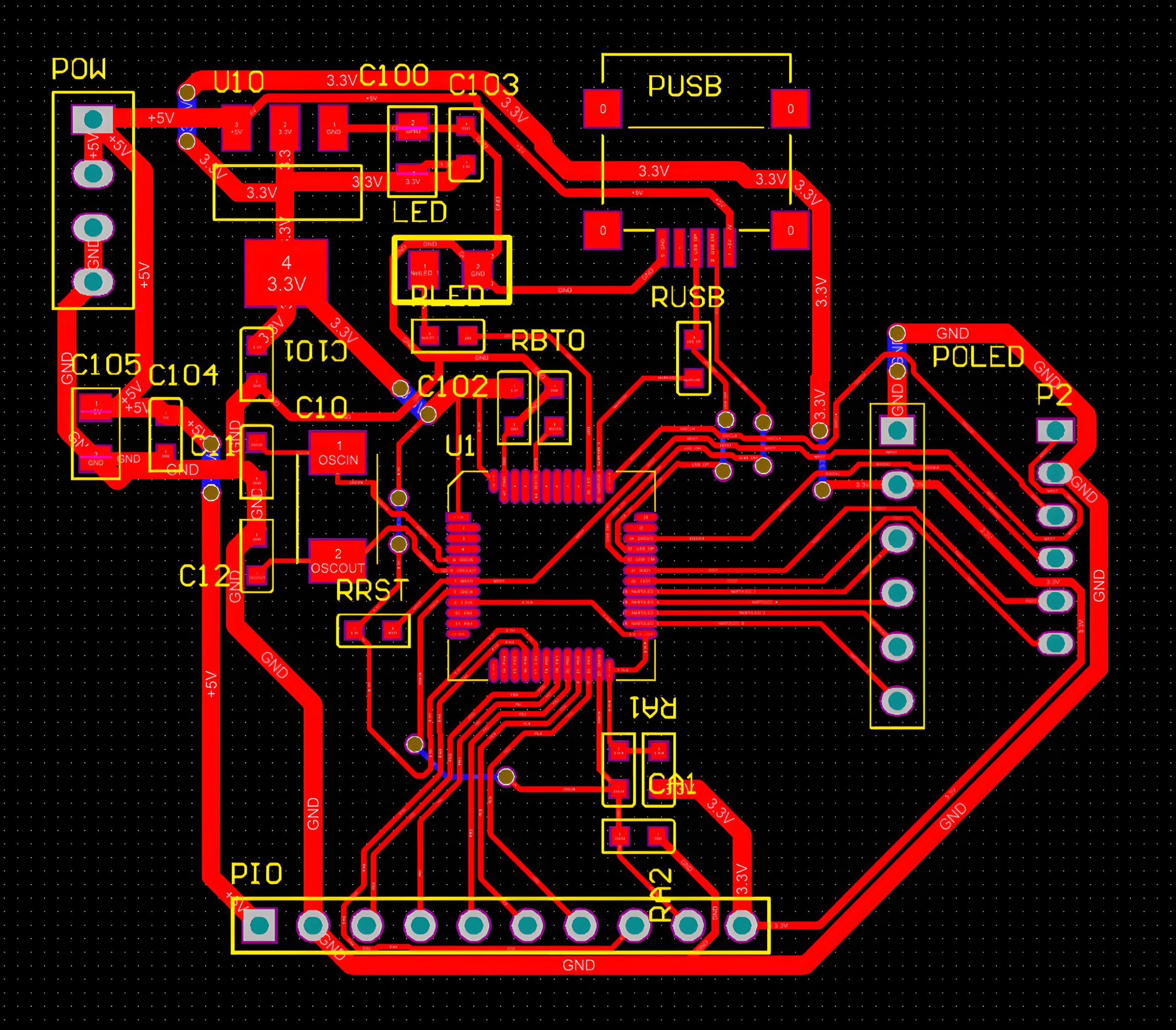
5. Label Everything Clearly
Proper labeling helps with assembly, testing, and future troubleshooting. Best practices include:
- Silkscreen component names and pin labels near connectors.
- Use clear reference designators (e.g., U1, C3, J1).
- Add a board version number and date code for tracking.
- Include a polarity mark on capacitors, LEDs, and connectors.
If space allows, consider printing your company logo or board name for easy identification.
6. Add Test Points and Debug Options
Testing is easier when you plan for it. Add the following features:
- Test points for important power rails, ground, and signals.
- Jumpers or configuration switches if the board supports multiple modes.
- Debug headers for I2C, UART, or SPI if microcontrollers are involved.
These additions slightly increase cost but save hours during development and field servicing.
7. Use Standardized Interfaces Where Possible
If your daughter board will be reused or shared across multiple projects, stick to standard connectors and pinouts. Some popular standards include:
- Raspberry Pi GPIO
- Arduino headers
- PCIe, USB, or M.2 interfaces
- Flat Flex Cable (FFC) connectors
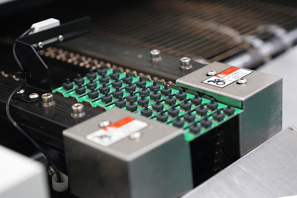
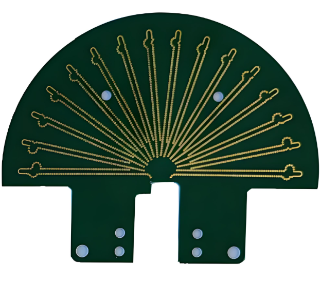
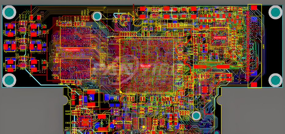
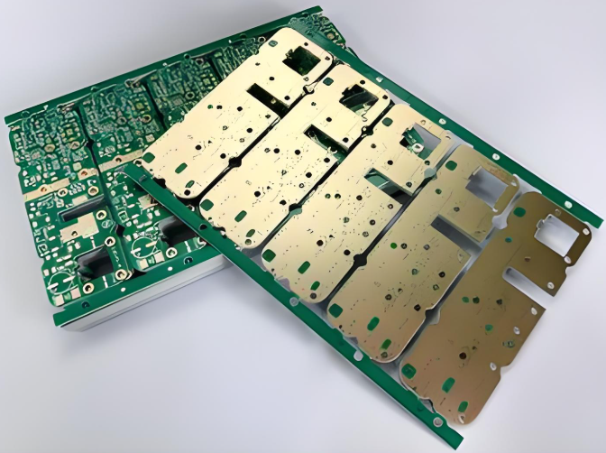
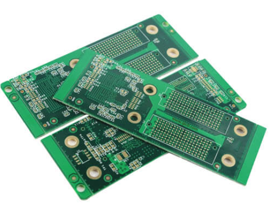
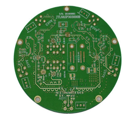
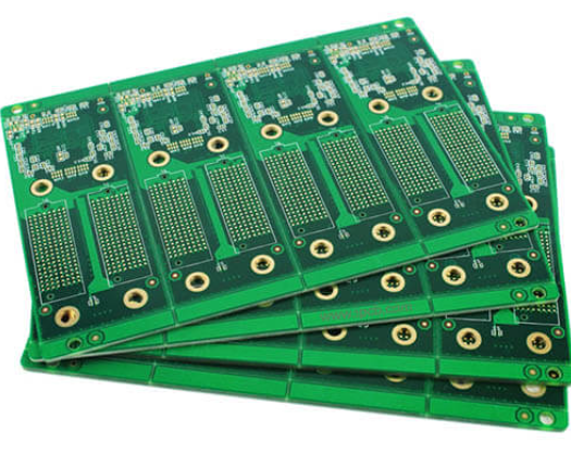
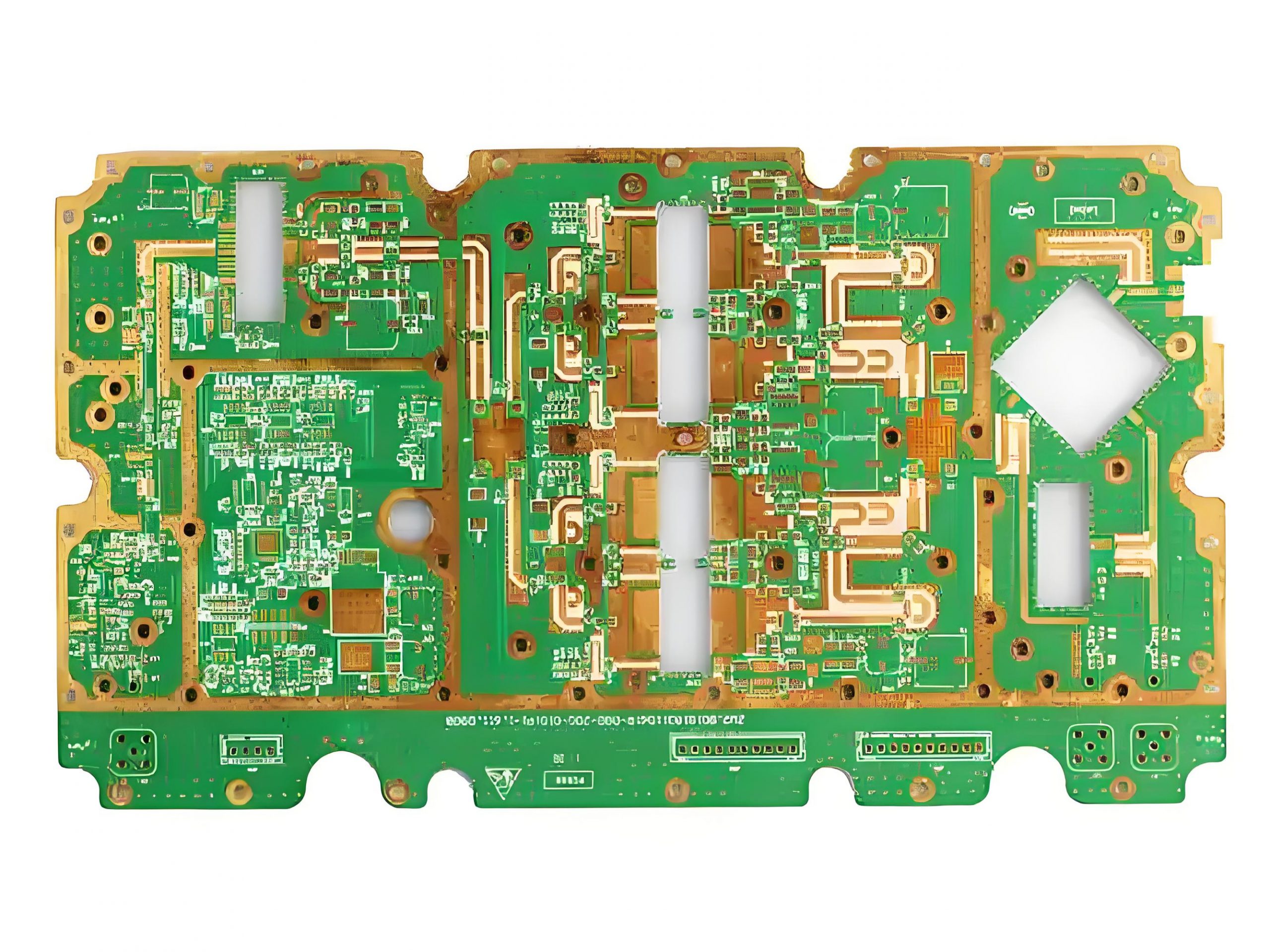
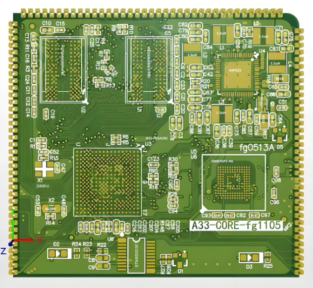
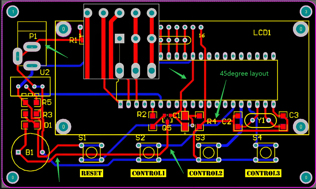
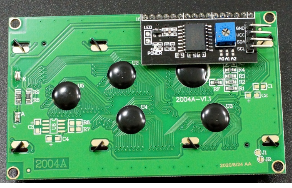
Standardization improves compatibility, reduces the chance of pin mismatch, and simplifies replacement in the future. Below is a typical daughter board picture and its internal parts:
8. Document Everything
Lastly, create full documentation before production. This should include:
- Schematic diagram
- Bill of materials (BOM)
- Gerber files and drill files
- Assembly drawings and 3D models
- Test procedure, if applicable
Proper documentation ensures that your manufacturer and QA team can assemble and verify the board without confusion.
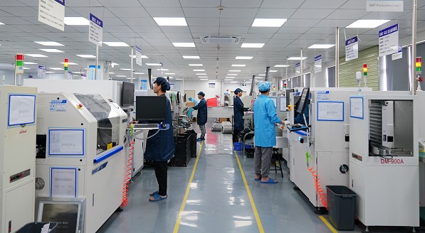
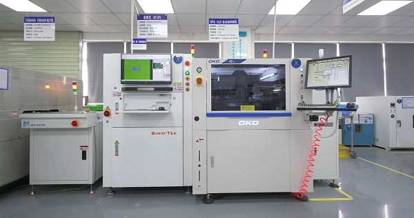
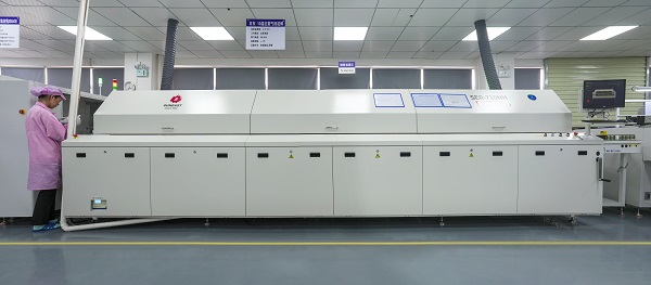
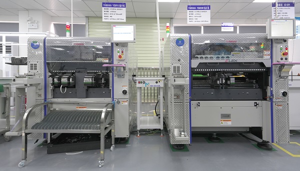
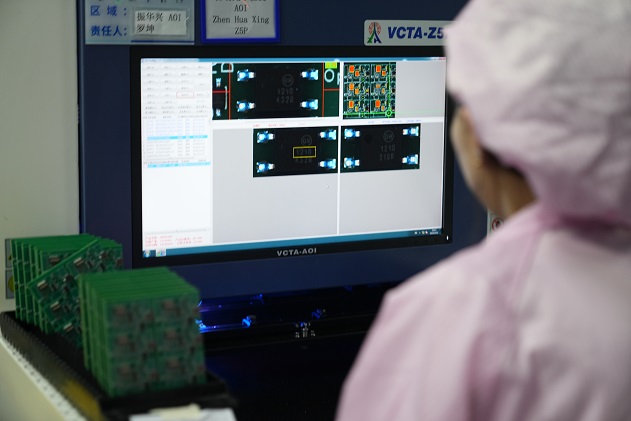
How EBest Circuit (Best Technology) Helps You?
When you’re developing daughter board PCBs, you want a manufacturing partner who understands your needs. EBest Circuit (Best Technology) brings reliability, fast lead times, and engineering support to every order. We provide professional design reviews for daughter board projects. Our engineers can help verify your connector choices, check your layout for manufacturability, and guide you in selecting cost-effective materials. We also offer PCB prototyping and small-batch PCB production so you can test your design before full rollout. Here’s how we help:
- One-stop PCB services: From layout to fabrication and assembly.
- Design guidance: Connector selection, board outline, and thermal layout advice.
- Full component traceability during production.
- Fast prototyping and volume production: Short delivery times with stable quality.
- Competitive pricing: Transparent quotes with no hidden fees.
With rich experience in daughter board manufacturing, we support applications in medical, automotive, industrial, and more.
If you’re planning your next daughter board PCB project, feel free to contact us for expert advice and a free quote.
FAQs
1. Can I reuse daughter boards across different systems?
If the interface and power requirements match, you can often reuse them. That’s one of the big advantages of modular boards.
2. What connectors are best for daughter boards?
Common choices include board-to-board headers, card-edge connectors, and mezzanine sockets. The choice depends on current rating and mechanical space.
3. Can I order a prototype of my daughter board before full production?
Yes. EBest Circuit (Best Technology) offers quick-turn prototyping for testing and validation.
4. Do daughter boards need firmware?
Only if they contain microcontrollers or programmable components. Otherwise, they act as hardware extensions.
5. Is it possible to add a daughter board later after initial product release?
Yes. That’s the beauty of modular design—it allows upgrades or extensions without redesigning the main system.