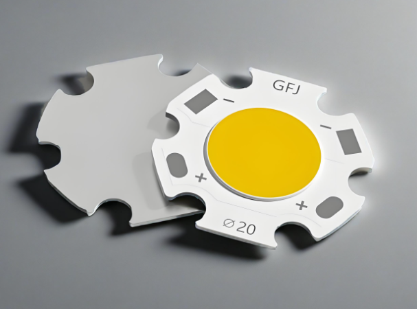
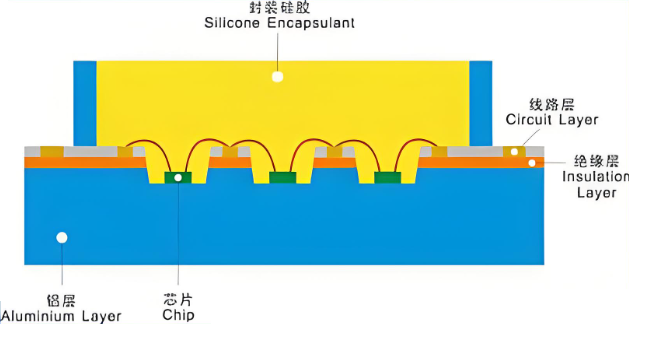
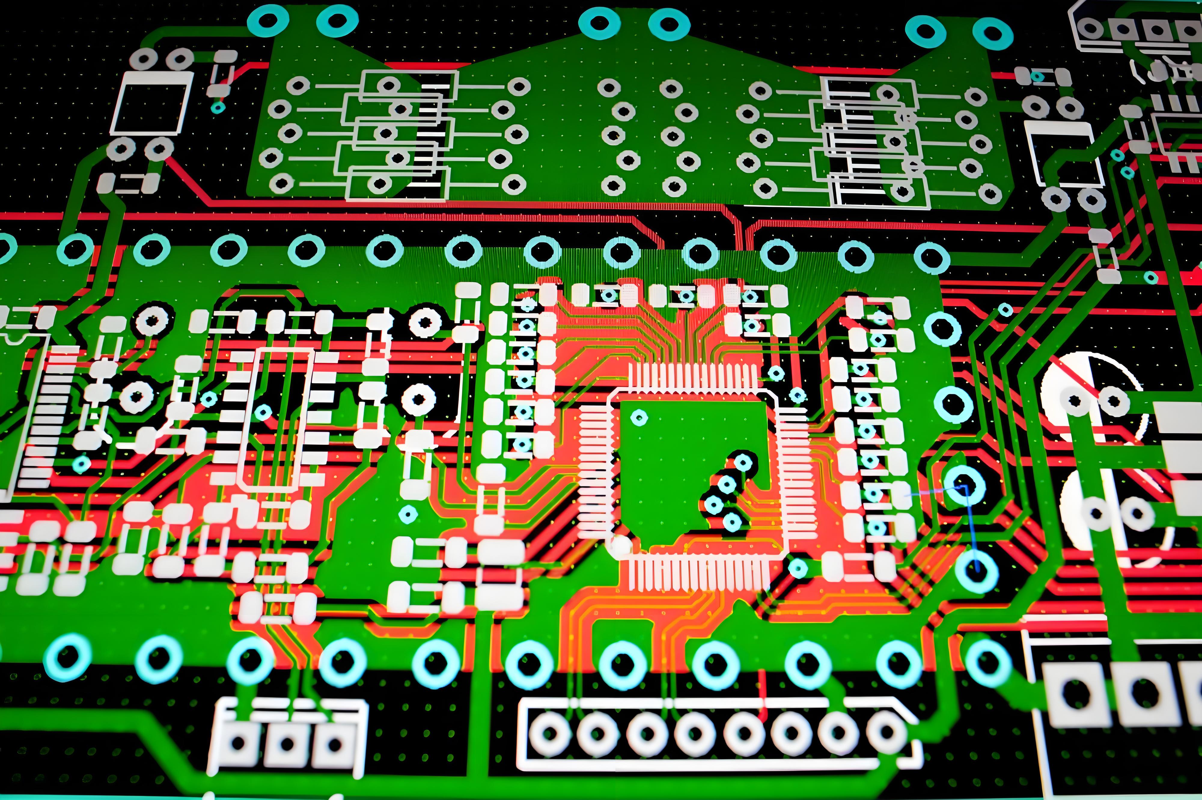
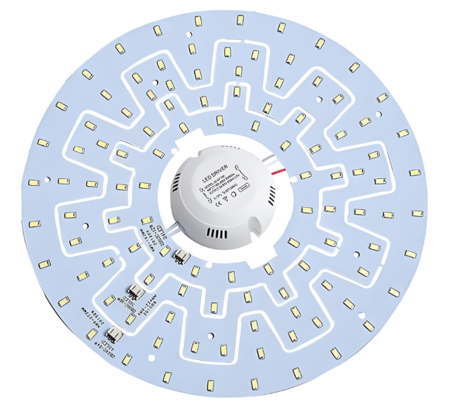
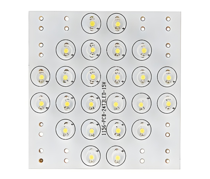
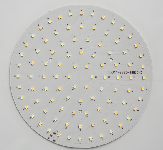
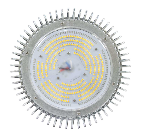
Heat is the invisible enemy of modern electronics. As devices shrink and power densities soar, efficient thermal management becomes non-negotiable. Metal-clad printed circuit boards (MCPCBs), using aluminum or copper bases, are workhorses for heat dissipation in applications like high-power LEDs, motor drives, and power supplies. Yet, a critical but often overlooked factor lurks within their layered structure: the thickness of the dielectric adhesive layer bonding the circuit to the metal base. This seemingly thin film holds immense power over your thermal performance. Let’s dissect why.
The Core Problem: The Adhesive Layer is a Thermal Bottleneck
The fundamental reason adhesive thickness matters boils down to physics: Thermal Resistance. Heat generated by components (like LEDs or MOSFETs) must travel through the adhesive layer to reach the highly conductive metal base (substrate), which then spreads and dissipates it into the environment (via heatsinks, convection, etc.).
Adhesive materials, even thermally conductive ones (often called Thermal Interface Materials – TIMs), possess thermal conductivity (measured in W/mK) orders of magnitude lower than the copper traces or the aluminum/copper base. For example:
- Aluminum: ~200 W/mK
- Copper: ~390 W/mK
- Typical Thermally Conductive Adhesive: 1.0 – 4.0 W/mK (though some advanced formulations reach 8-10+ W/mK)
This adhesive layer is inherently the highest thermal resistance point in the primary heat path from the component junction to the ultimate heat sink.
How Thickness Amplifies the Thermal Bottleneck?
The thermal resistance (R_th) of the adhesive layer itself is governed by a simple, yet critical formula:
R_th_adhesive = L / (k * A)
Where:
- R_th_adhesive = Thermal Resistance of the adhesive layer (°C/W or K/W)
- L = Thickness of the adhesive layer (meters)
- k = Thermal Conductivity of the adhesive material (W/mK)
- A = Cross-sectional area for heat flow (square meters)
This equation reveals the devastating impact of thickness:
- Direct Proportionality (R_th ∝ L): Thermal resistance increases linearly with adhesive thickness. Double the thickness, double the thermal resistance. This is the most significant and direct effect. Thicker adhesive creates a longer path for heat to travel through a poorly conducting material, significantly hindering flow.
- Consequence: Higher component operating temperatures (Tj), reduced efficiency, accelerated aging (lumen depreciation in LEDs, shorter lifespan), and potential reliability failures.
- Exacerbating Low Conductivity (R_th ∝ 1/k): While k is a material property, the impact of a low k is magnified as thickness increases. A poor adhesive (k = 1.0 W/mK) at 100μm thickness creates much higher resistance than a good adhesive (k = 3.0 W/mK) at the same thickness. Making the layer thicker worsens the penalty for using a low-conductivity material. Optimizing both k and L is crucial.
- Increased Interface Resistance: Heat doesn’t flow perfectly across material boundaries. Microscopic imperfections (roughness, voids, poor wetting) at the interfaces between the component/circuit and the adhesive, and between the adhesive and the metal base, create additional “contact resistance.” While primarily dependent on surface quality and pressure, a thicker layer can sometimes make it harder to achieve optimal intimate contact at both interfaces simultaneously, potentially increasing the effective total interface resistance.
- Extended Heat Path: Thickness literally increases the distance heat energy must travel via conduction through the resistive adhesive material before reaching the highly conductive metal substrate. This longer path inherently slows down heat transfer.
Optimizing for Superior Thermal Performance
Achieving the best possible thermal performance requires a holistic approach targeting adhesive thickness, material properties, and manufacturing quality:
- Minimize Thickness (L): This is priority #1.
- Process Control: Implement rigorous process controls during lamination (pressure, temperature, vacuum) to achieve consistent, ultra-thin bond lines. Advanced techniques like controlled-flow adhesives and precise pressure profiling are key.
- Material Selection: Choose adhesives specifically formulated for thin application while maintaining dielectric strength and reliability. Some resin systems (e.g., certain epoxies) inherently allow for thinner layers than others.
- Target Range: Strive for adhesive layers in the range of 50μm to 100μm (2-4 mils) where possible, balancing thermal performance with manufacturability and dielectric requirements. Going below 50μm requires exceptional process control.
- Maximize Thermal Conductivity (k):
- Filler Technology: Thermally conductive adhesives rely on ceramic fillers (Al₂O₃, AlN, BN, SiO₂) within a polymer resin. Higher filler loading increases k but impacts viscosity and processability. Seek formulations with optimal filler type, size distribution, and loading for maximum k.
- Advanced Fillers: Consider adhesives using higher-performance (though often more expensive) fillers like Aluminum Nitride (AlN) or Boron Nitride (BN) which offer significantly higher intrinsic conductivity than standard Alumina (Al₂O₃).
- Verified Data: Demand certified k values measured using standardized methods (e.g., ASTM D5470), not just vendor claims.
- Optimize Interface Quality:
- Surface Preparation: Ensure excellent cleanliness and appropriate surface roughness/treatment on both the circuit side (usually copper) and the metal base side prior to lamination to promote optimal wetting and adhesion.
- Void Elimination: Minimize air bubbles/voids trapped within the adhesive or at interfaces. Use vacuum lamination processes and adhesives with good flow characteristics.
- Uniformity: Achieve highly uniform adhesive thickness distribution across the entire board area. Localized thick spots are significant thermal bottlenecks.
- Holistic Design & Material Synergy:
- Component Placement: Place high-heat-dissipation components directly over areas of the metal base with the best thermal connection (minimal vias/cutouts underneath).
- Copper Weight: Use thicker copper layers (e.g., 2oz, 3oz) on the circuit layer to spread heat laterally before it enters the adhesive, reducing the effective thermal gradient across the adhesive.
- Metal Base Choice: For extreme applications, consider copper bases (higher k than aluminum) to further reduce the substrate’s spreading resistance once heat finally reaches it.
The Designer’s Checklist for Thermal Success:
- Specify Adhesive Thickness: Don’t leave it as an afterthought. Define a maximum allowable thickness requirement in your MCPCB specs (e.g., “Adhesive Layer: ≤ 75μm”).
- Demand Certified k Value: Require adhesive suppliers or PCB manufacturers to provide reliable thermal conductivity data.
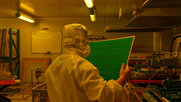
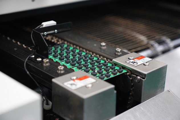
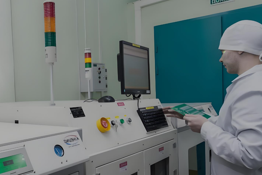
- Prioritize Process Capability: Choose a PCB manufacturer with proven expertise and tight process controls for thin, uniform, void-free adhesive layers. Ask about their lamination process, quality control measures (e.g., ultrasonic scanning for voids), and typical thickness consistency.
- Consider Total Thermal Resistance (R_th(j-a)): Ultimately, evaluate the entire thermal path from component junction to ambient. While minimizing adhesive R_th is critical, also ensure efficient heat sinking beyond the PCB.
Conclusion: Thin is In (for Thermal Performance)
In the high-stakes game of thermal management within metal-clad PCBs, the thickness of the dielectric adhesive layer is not a minor detail; it’s a primary performance dictator. Its inherently low thermal conductivity means that even small increases in thickness dramatically raise thermal resistance, directly leading to hotter components and compromised reliability.
By understanding the physics (R_th = L / (k * A)), focusing relentlessly on minimizing thickness through advanced materials and precise manufacturing, maximizing thermal conductivity, and ensuring perfect interfaces, engineers can unlock the full heat-spreading potential of their metal substrates. Ignoring the adhesive layer’s thickness is a surefire way to let thermal problems silently undermine your product’s performance and lifespan. Prioritize thinness, prioritize thermal conductivity, prioritize quality – your components will thank you with cooler operation and longer life.