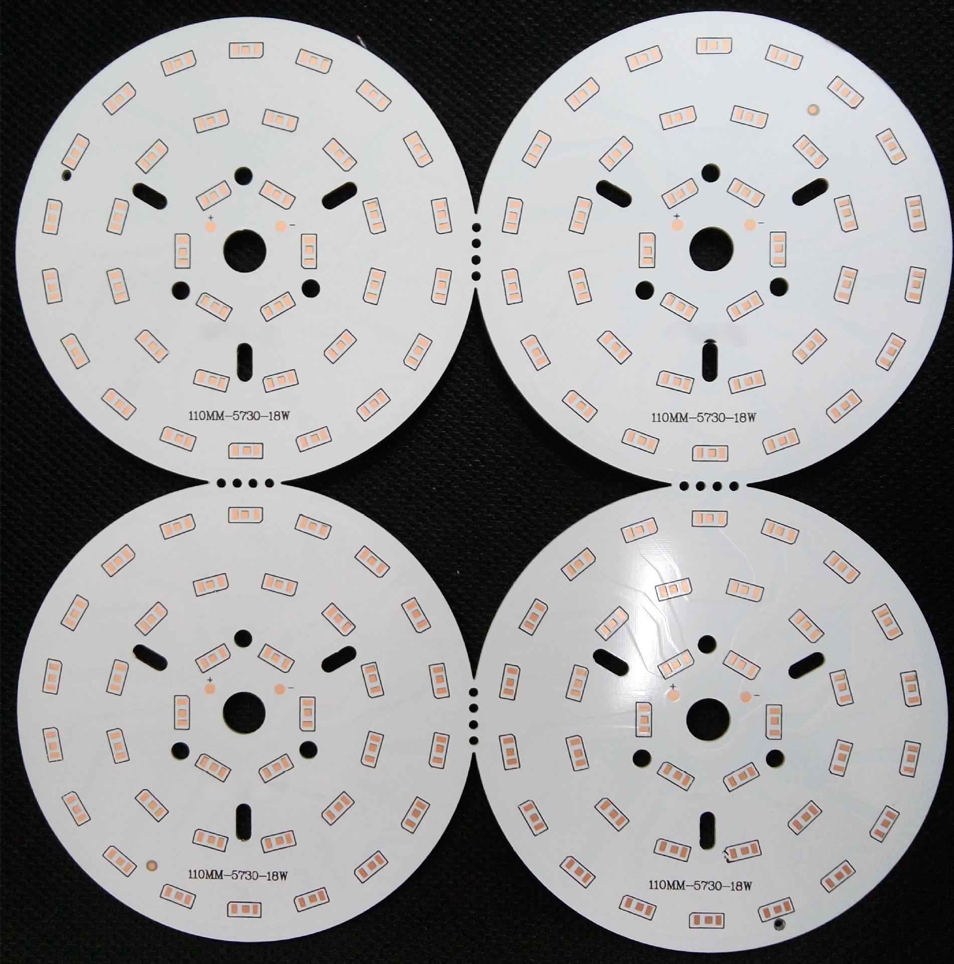
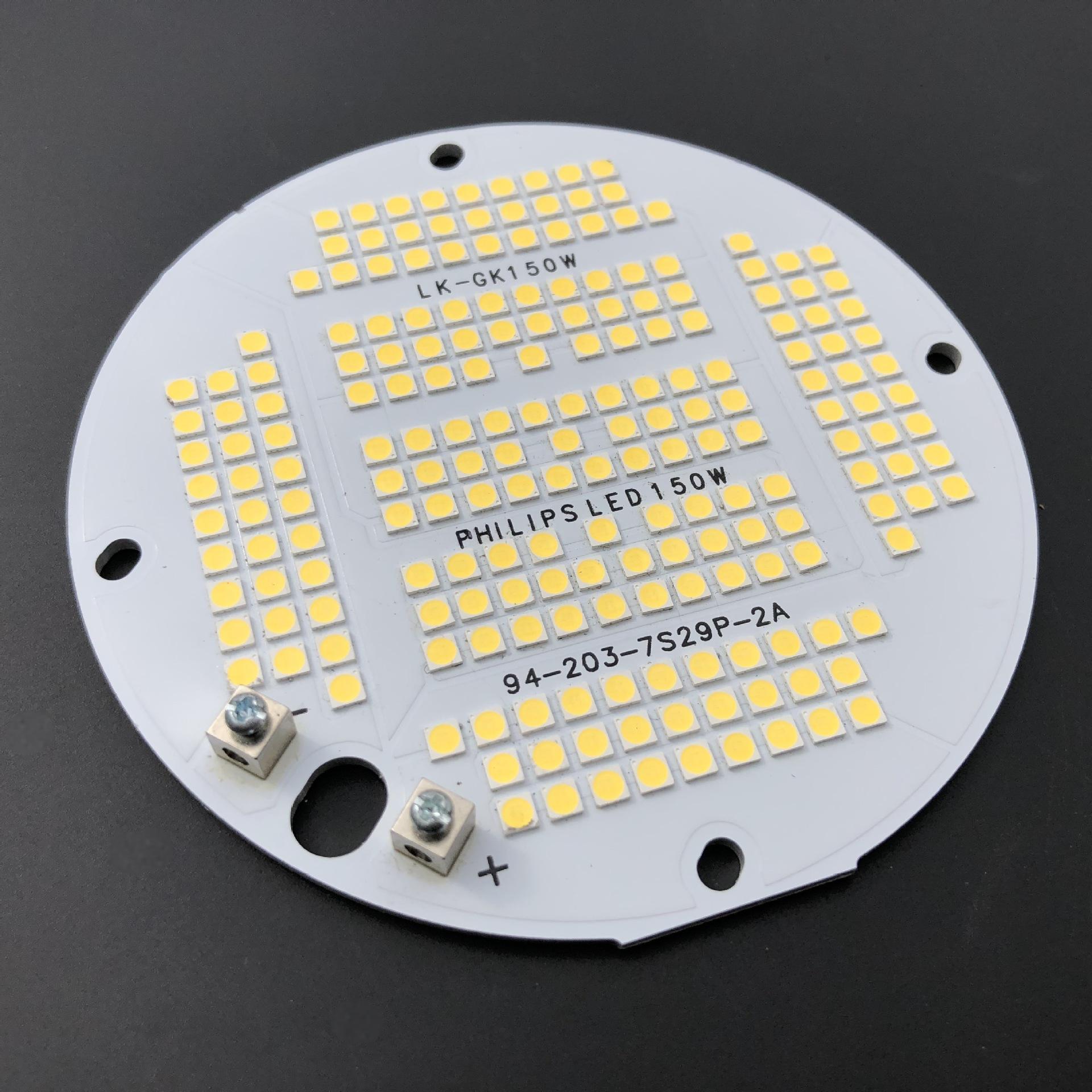
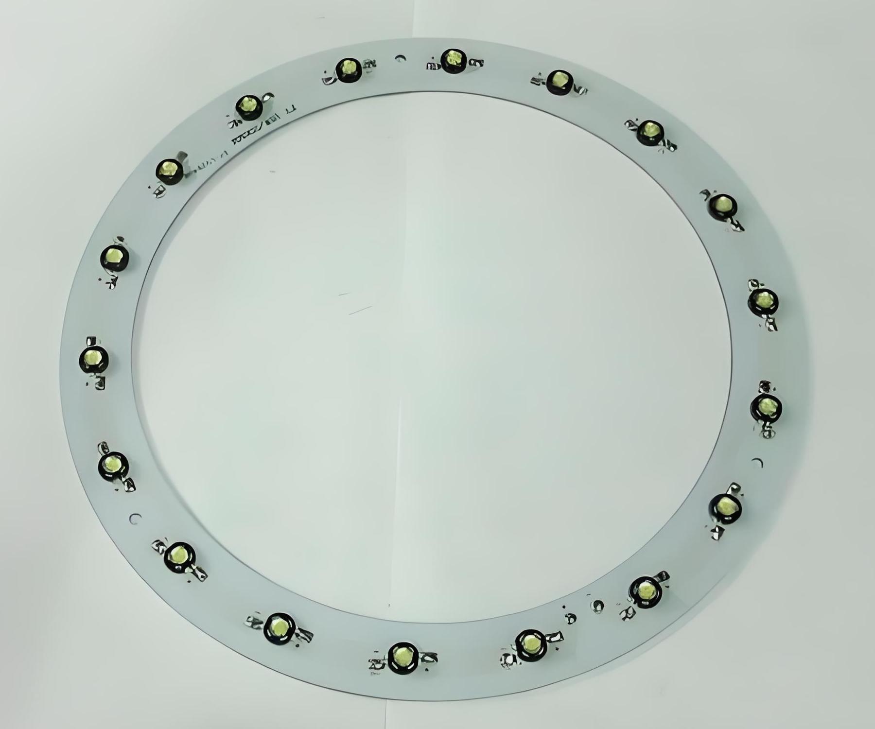
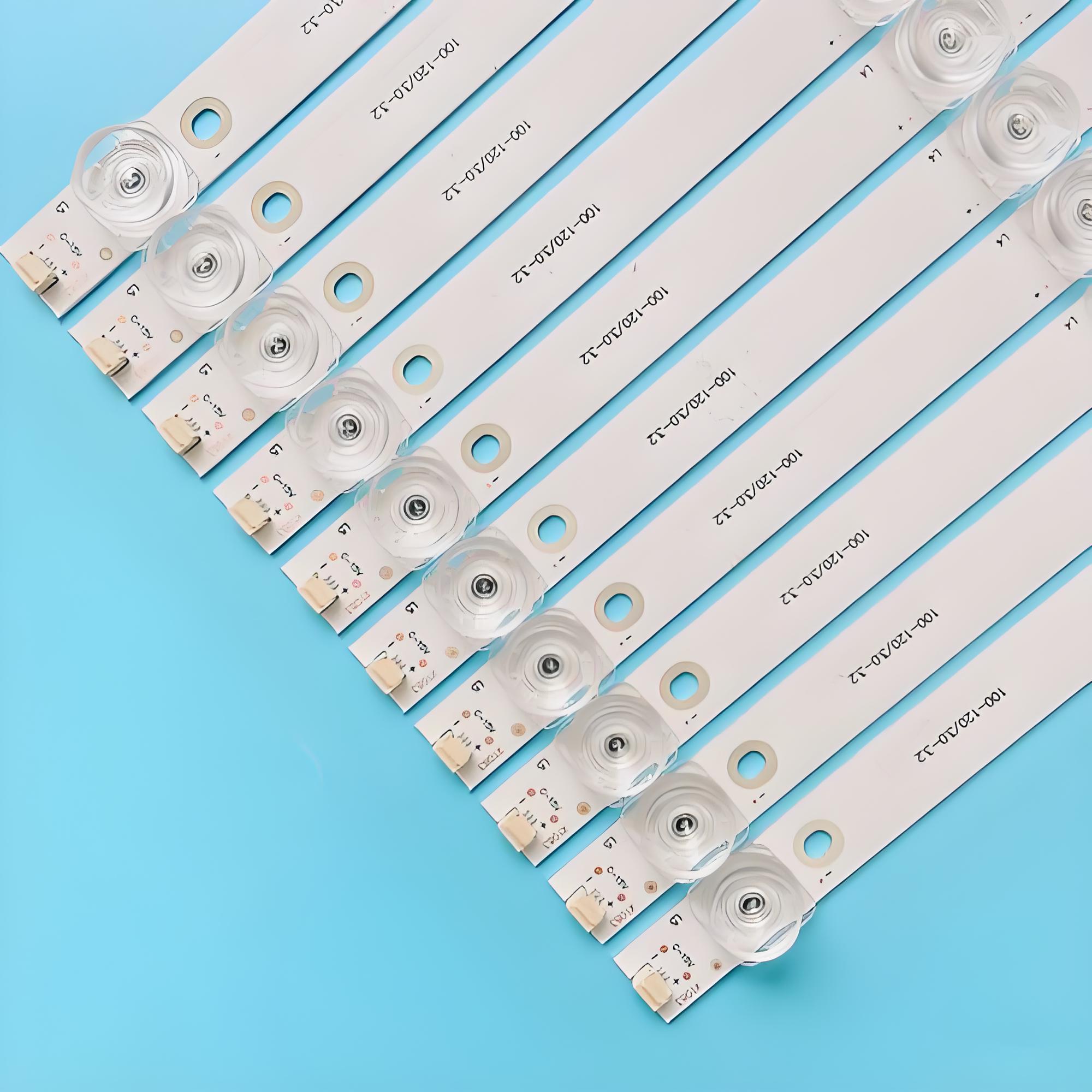
An MCPCB LED strip is an LED light strip built on a Metal Core PCB instead of a regular fiberglass board. The metal base, usually aluminum, helps pull heat away from the LEDs. This keeps them cooler, brighter, and longer-lasting.
What is MCPCB LED?
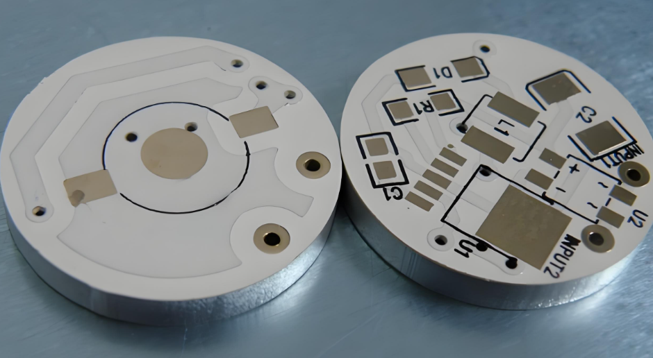
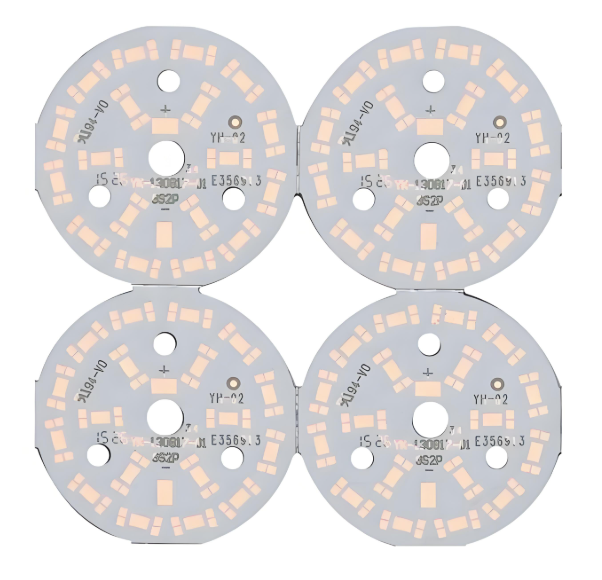
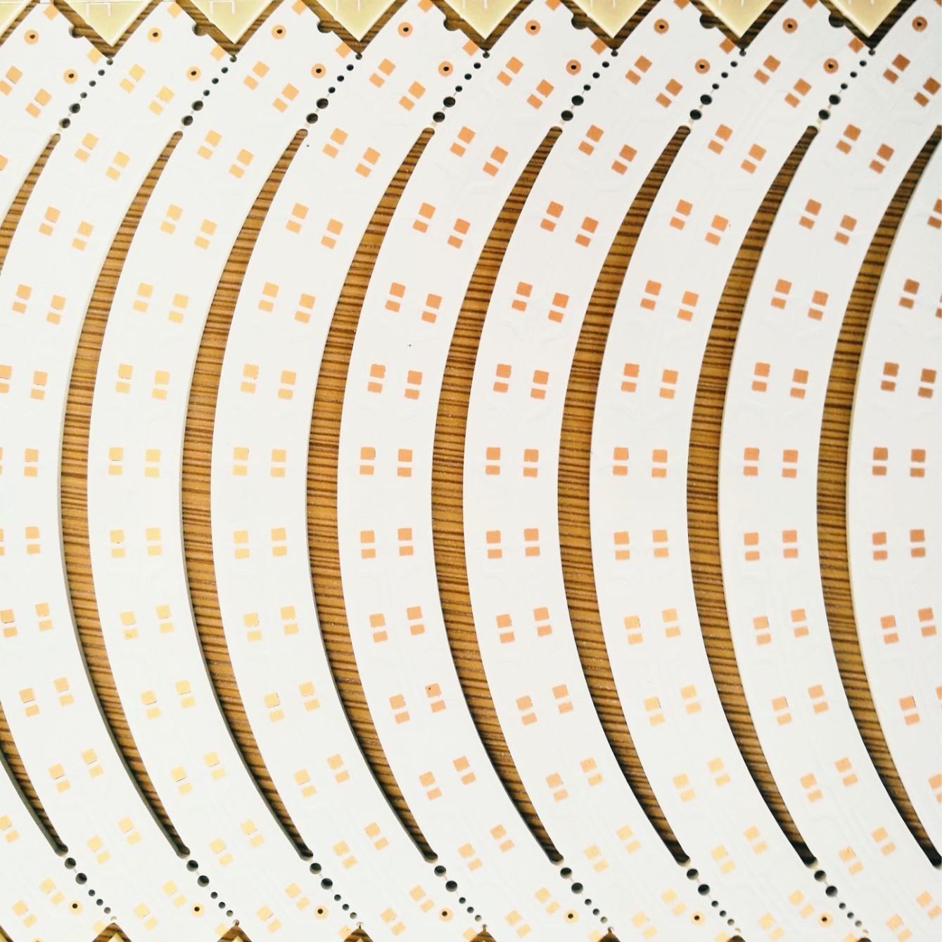
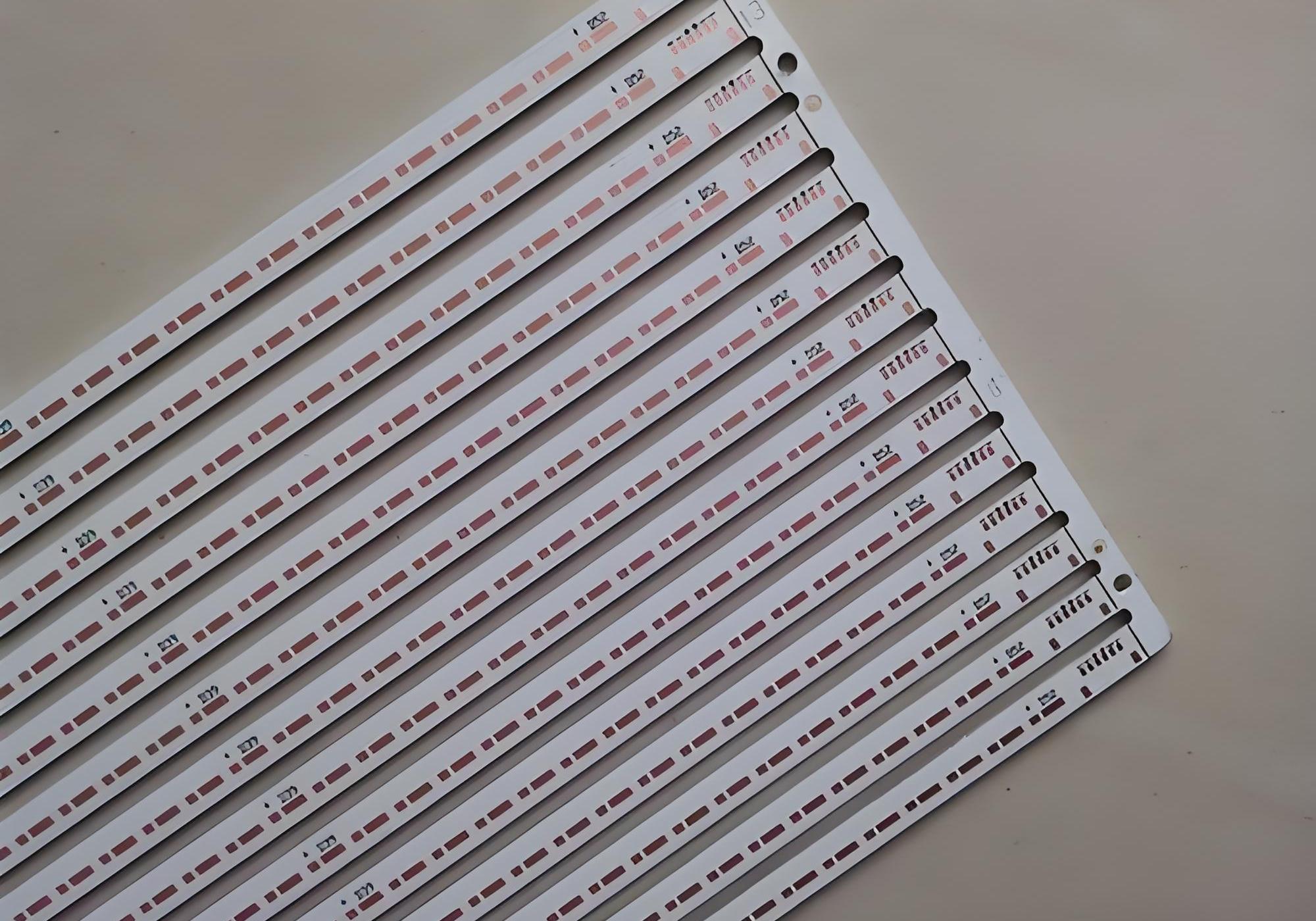
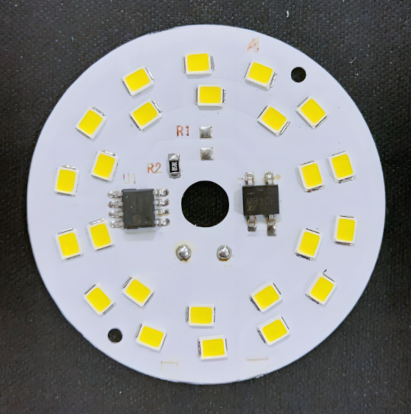
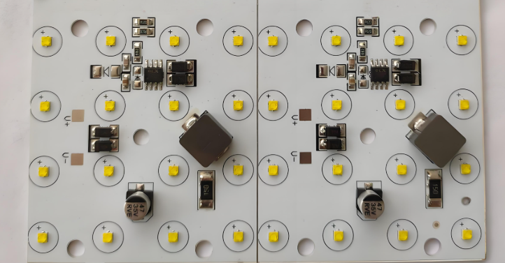
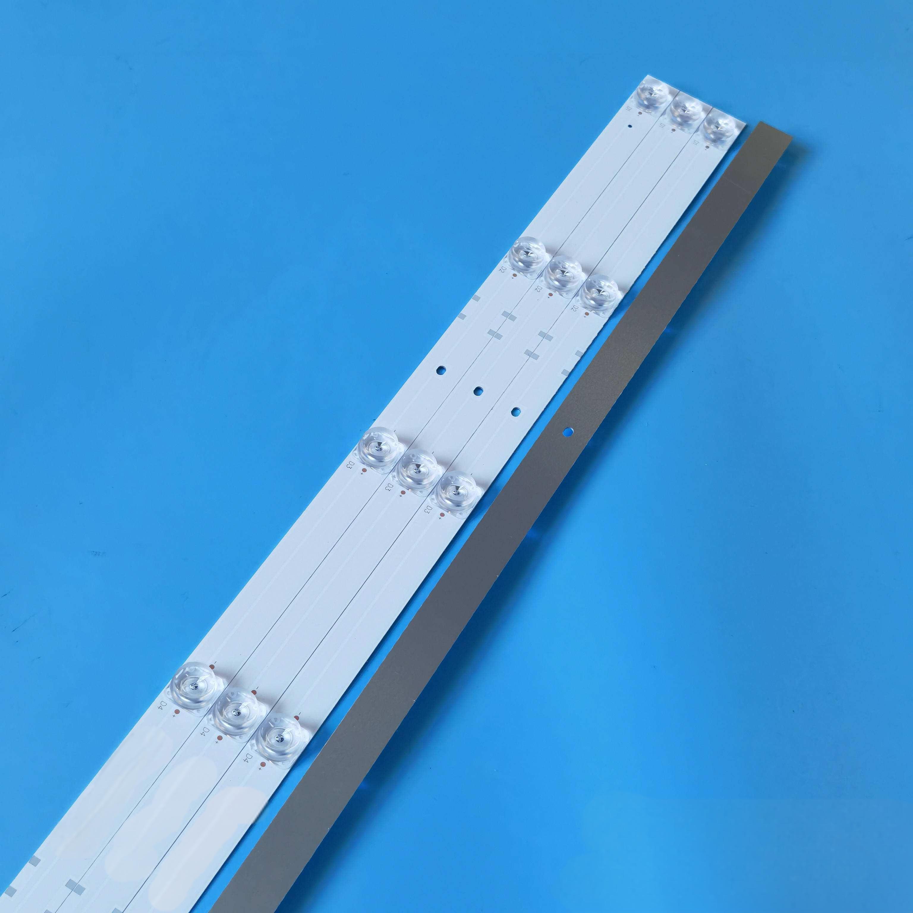
An MCPCB LED strip is a flexible or rigid lighting circuit that uses Metal Core Printed Circuit Boards (MCPCB) instead of traditional fiberglass boards. These boards are made with a metal base—often aluminum—layered with a dielectric material and topped with copper circuitry.
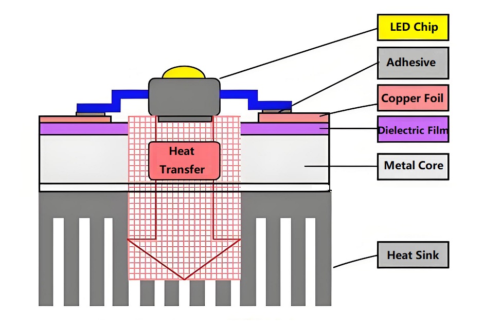
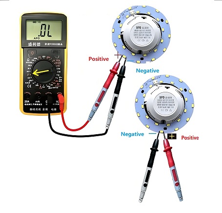
The main advantage? Superior heat dissipation. LED chips generate heat, and if it’s not managed properly, brightness fades and lifespan drops. The metal core acts as a thermal bridge, quickly pulling heat away from the LEDs.
Why use MCPCB for LED strip lights?
LED light strips are widely used for their compact size and bright output, but they also bring a problem: heat. Excessive heat shortens LED life, dims the light, and can even cause circuit failure.
Here’s where MCPCB LED steps in with its unique benefits:
- High thermal conductivity: Metal cores rapidly remove heat from LED chips.
- Longer lifespan: Cooler LEDs mean longer use.
- More stable output: No flickering or fading over time.
- Compact design support: Even tight spaces can house high-powered LEDs safely.
- Durability: Metal cores are more resistant to physical damage than FR4 boards.
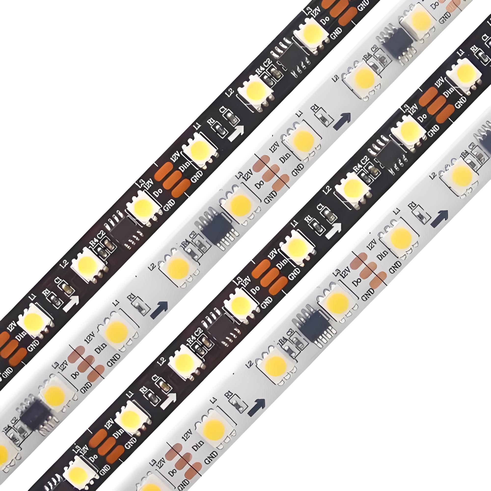
How does MCPCB design affect LED strips?
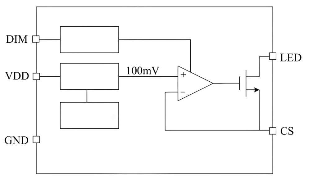
The MCPCB design is more than just the layout of circuits. Each layer of the MCPCB is chosen and designed for a specific function:
- Metal base (usually aluminum): Carries the heat away.
- Dielectric layer: Transfers heat while keeping electrical isolation.
- Copper circuit layer: Routes electricity to the LEDs.
Even the thickness of the dielectric layer impacts how fast heat can move. A thinner dielectric means faster transfer, but it must still insulate properly. Similarly, thicker copper can handle higher currents without overheating.
Good MCPCB design ensures even temperature distribution. That means no LED on the strip gets too hot. Even light, long life, and better performance.
Can MCPCB design improve LED lifespan?
Absolutely. Heat is the main enemy of LED lifespan. Every degree of temperature rise reduces the life of an LED chip.
Traditional PCB materials like FR4 don’t handle heat well. Over time, they allow hotspots to build up. These hotspots degrade the LED’s light output and can eventually cause failure.
But MCPCB design changes the game. By channeling heat away from the LED source, it keeps the chip temperature lower. This cooler environment means:
- No yellowing of lenses
- No cracking of solder joints
- No degradation of LED chip efficiency
So yes, MCPCB LED strips don’t just shine brighter—they shine longer.
MCPCB LED vs. regular LED PCB strip – what’s better?
Let’s compare a regular LED PCB strip to a metal core version:
| Feature | Regular LED Strip (FR4) | MCPCB LED Strip |
| Heat dissipation | Poor | Excellent |
| Brightness over time | Decreases | Maintained |
| Durability | Fragile | Rugged |
| Power handling | Low | High |
| Cost | Lower upfront | Better long-term value |
While FR4-based LED strips may seem cost-effective, they often end up needing frequent replacements—especially in high-power applications. MCPCB LED strips, on the other hand, are built to last.
How to choose the right LED PCB strip?
Choosing the right LED PCB strip depends on your application. Here are a few factors to consider:
- Heat Load: If your strip is in a confined or warm space, go for MCPCB.
- Power Requirement: More power means more heat. MCPCB handles high current safely.
- Installation Area: Metal core strips are ideal for industrial, automotive, and high-brightness home uses.
- Budget vs. Longevity: While MCPCB may cost more upfront, it saves money in the long run.
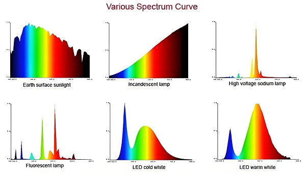
- Brightness and Color Consistency: Heat can affect color temperature. MCPCB avoids this.
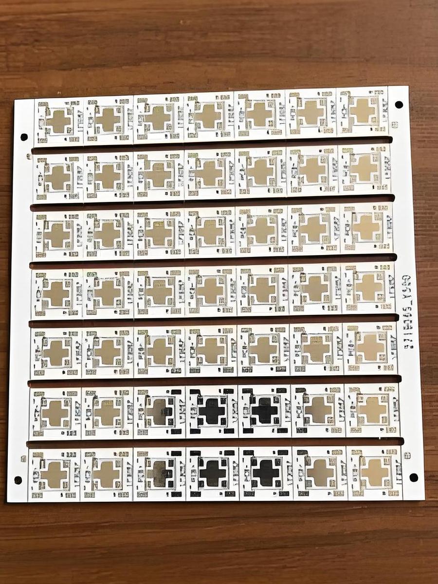
How to customize an MCPCB LED strip?
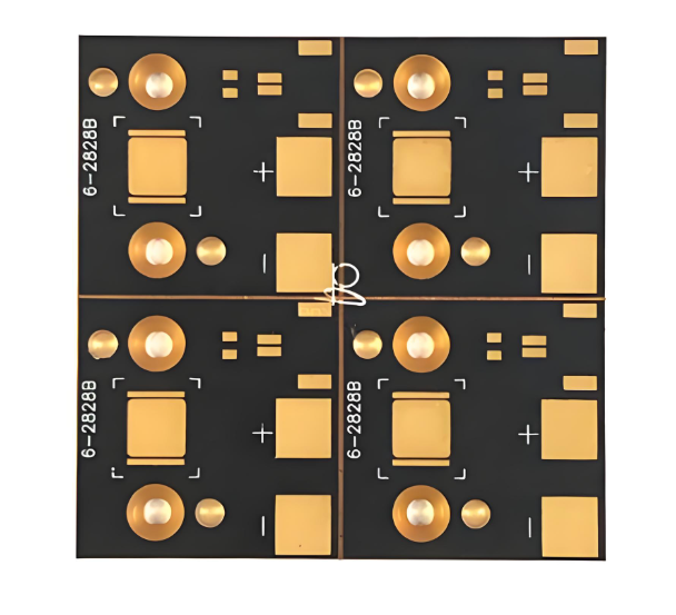
Customization is one of the most important aspects of MCPCB design. With the right manufacturer, you can tailor almost everything:
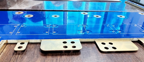
- Board size and shape: Fit into curves, tight corners, or irregular enclosures.
- Copper thickness: For heavy-duty current or low-voltage precision.
- Thermal conductivity: Select different dielectric materials for performance.
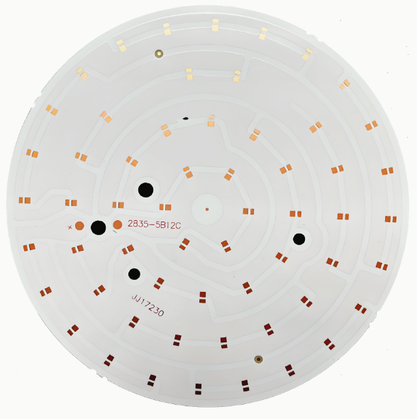
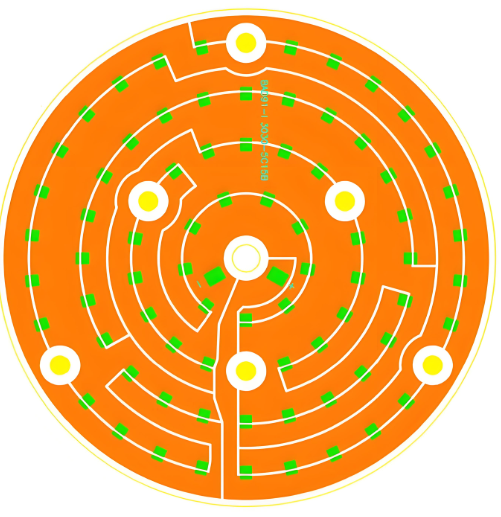
- LED configuration: Control spacing, brightness, and light pattern.
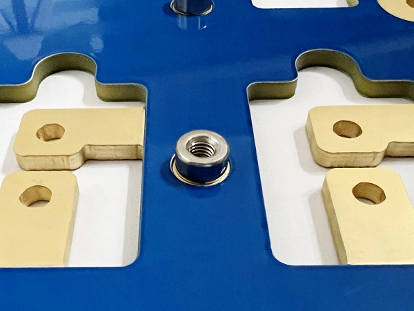
- Mounting features: Add connectors, screw holes, or adhesive backs.
- Surface finish: Choose between ENIG, HASL, OSP for different protection levels.
When you work with a professional manufacturer like EBest Circuit (Best Technology), your custom MCPCB LED strip lights will be the best they can be.
Where is MCPCB LED used most?
You’ll find MCPCB LED strips in places that demand both performance and reliability. Here are just a few common uses:
- Automotive lighting: Headlights, tail lamps, and interior accents.
- Commercial lighting: Display cases, signage, and architectural lights.
- Medical devices: Surgical lights and diagnostic equipment.
- Industrial machines: Workstation lighting, control panels.
- Consumer electronics: High-end flashlights, monitors, smart mirrors.
- Streetlights & floodlights: Large scale applications with heavy thermal loads.
Wherever durability meets brightness, MCPCB LED plays a vital role.
Conclusion:
MCPCB LED strips surpass traditional LED PCB light strips in every way with better heat management, longer lifespan, and greater durability.
Need support for MCPCB LED strip design or customization? Reach out to us at sales@bestpcbs.com