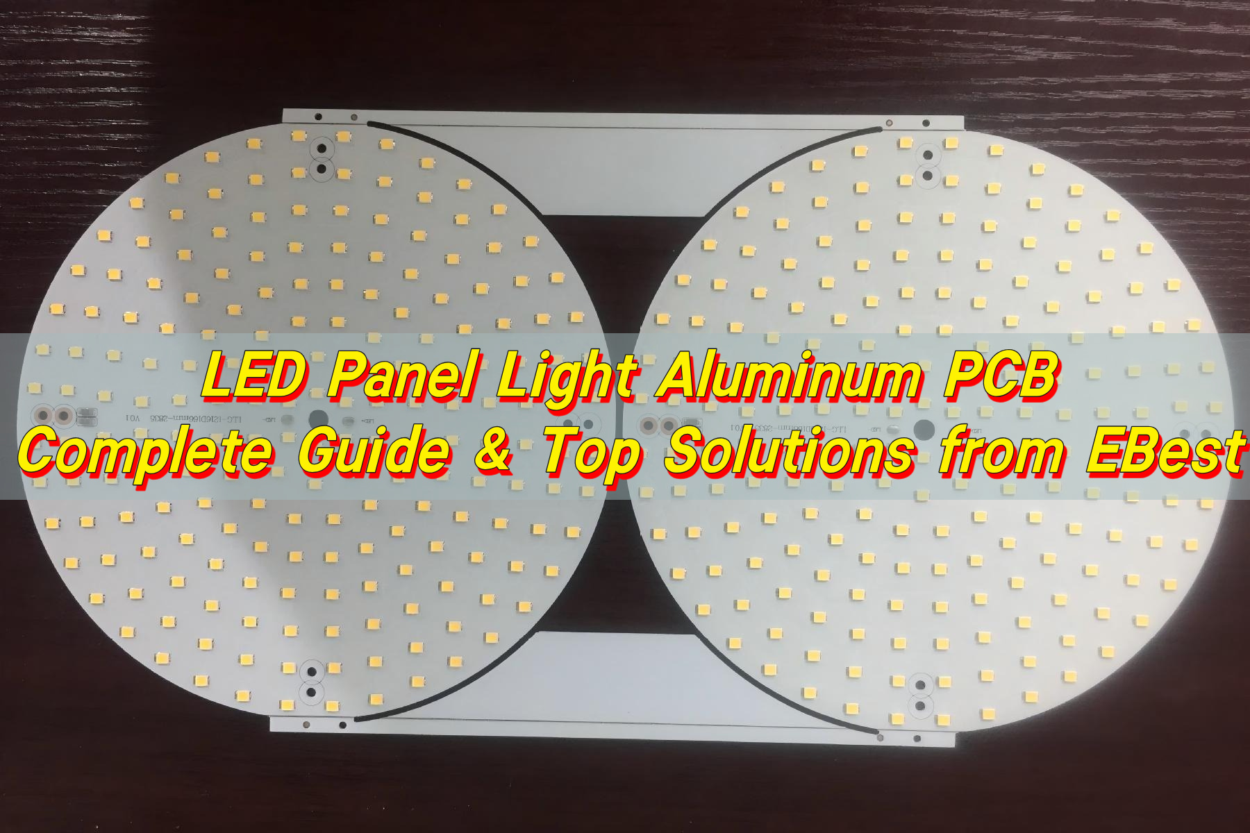
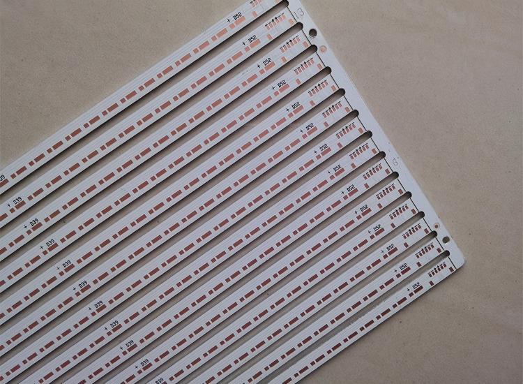
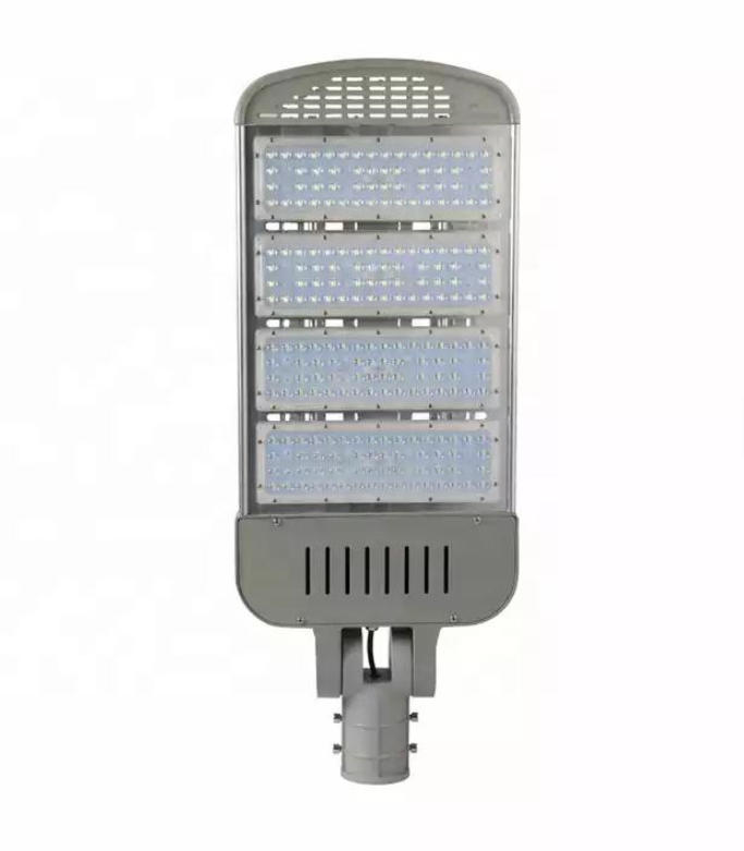
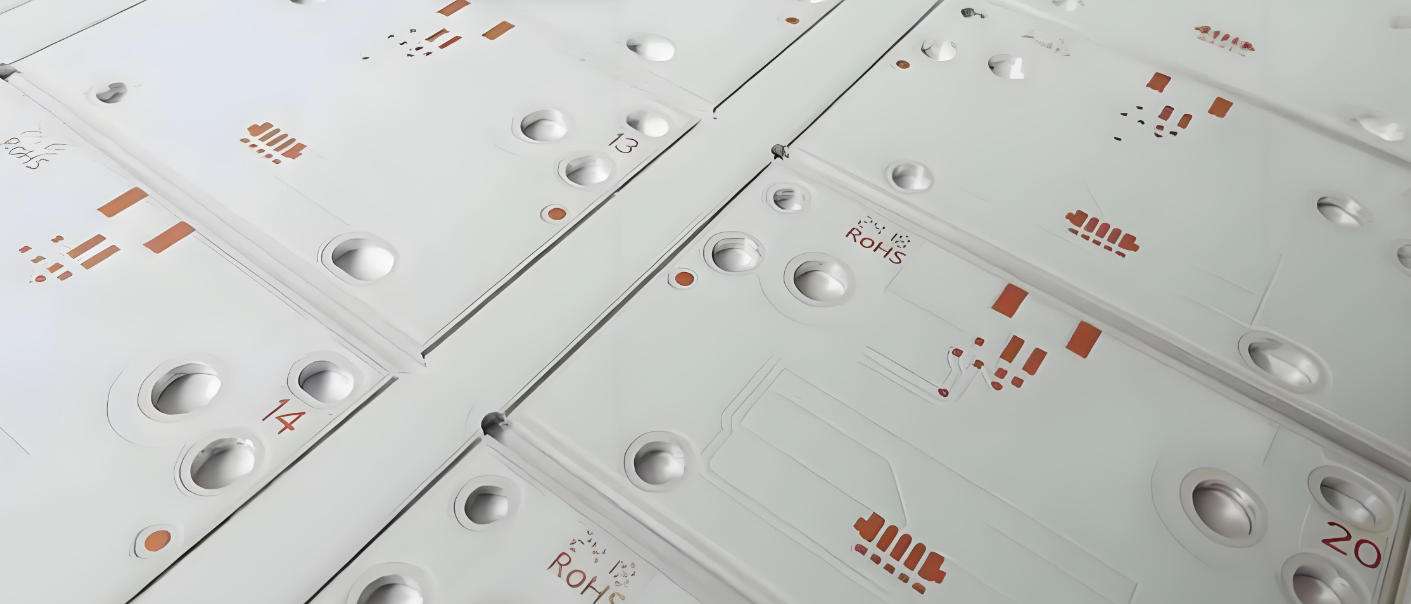
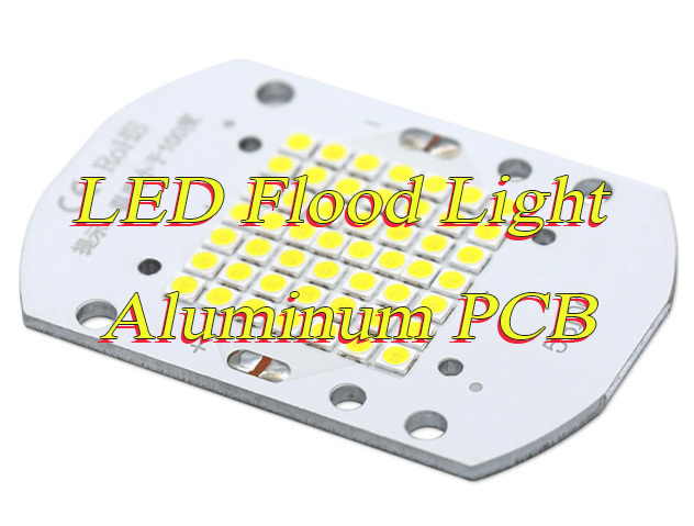
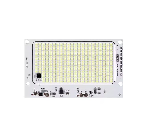
Are you struggling to find a durable, high-thermal LED flood light aluminum PCB that fixes outdoor lighting failures, uneven heat dissipation, and moisture damage for large-area outdoor projects? This guide covers the top pain points of standard outdoor PCBs, how premium aluminum PCB technology boosts thermal performance and fixture lifespan, practical tips for selection, installation and maintenance, key thermal specs for high-power flood lights, and common FAQs about LED flood light aluminum PCB and LED spotlight aluminum PCB. We also highlight EBest’s rigorously tested, IP67 waterproof aluminum PCBs with industry-leading thermal conductivity, extreme temperature resistance and custom adaptability to help you build reliable, long-lasting outdoor flood lighting with minimal downtime and maintenance.
Are You Facing these Challenges of LED Flood Light Aluminum PCB?
- Does your outdoor LED flood light suffer from uneven heat dissipation that causes dim, inconsistent lighting across large areas?
- Is moisture penetration damaging your flood light PCB during heavy rain or high-humidity outdoor conditions?
- Does poor thermal management lead to frequent LED fixture failures and shortened lifespan for your outdoor lighting?
- Are you struggling with PCB performance degradation in high-temperature outdoor environments during summer months?
- Do standard PCBs fail to support the high-power output needed for large-area outdoor flood lighting projects?
- Is uneven heat distribution causing color shifting or reduced brightness in your LED flood light panels?
Our Solution to the Above Challenges of LED Food Light Aluminum Circuit Board
- We use high-thermal-conductivity aluminum substrates to ensure uniform heat dissipation across the entire PCB surface, eliminating hotspots and uneven lighting.
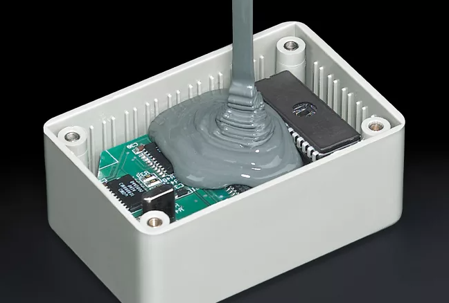
- Our aluminum PCBs feature a professional waterproof coating and sealed dielectric layers to block moisture penetration, even in heavy rain and high-humidity outdoor settings.
- Advanced thermal management design prevents overheating, reducing LED component wear and extending the overall lifespan of outdoor flood light fixtures.
- Reinforced aluminum construction maintains stable performance in extreme high and low outdoor temperatures, avoiding performance degradation in harsh weather.
- Optimized circuit layout and thick copper traces support high-power LED loads, perfectly matching the output requirements of large-area outdoor flood lighting.
- Precision-engineered thermal pathways ensure even heat distribution across the PCB, preventing color shifting and maintaining consistent brightness levels.
Why Choose EBest for Your LED Flood Light Aluminum PCB Manufacturer?
EBest is more than just a PCB supplier, we are a partner focused on solving your real-world pain points with LED flood light aluminum PCB, delivering solutions that protect your bottom line and boost long-term performance for outdoor large-area lighting projects. We specialize in premium LED spotlight aluminum PCB and LED flood light aluminum PCB built for harsh outdoor conditions, engineered to cut fixture failure rates by up to 85% compared to low-grade generic PCBs, while eliminating frequent maintenance downtime and short service lifespans. Our boards are fully resistant to heavy rainfall, extreme temperature swings from -40°C to 125°C, and prolonged outdoor exposure, letting you build durable lighting products that perform reliably year-round without constant replacements.
Our core advantage lies in superior thermal engineering that directly solves the biggest challenge of high-power outdoor flood lights: consistent, even heat dissipation. Backed by IPC industry standards, our aluminum PCBs boast a thermal conductivity of 2.0-4.0 W/(m·K) — nearly 7x higher than standard FR4 PCBs, which only offer 0.3 W/(m·K) thermal conductivity. Unlike generic boards that trap heat and cause LED chip temperatures to spike, speeding up light decay and burnout, our high-conductivity aluminum substrates and optimized thermal pathways pull heat away from LEDs instantly and spread it evenly across the entire board. This design keeps flood lights running at full, uniform brightness over large areas, cuts annual light decay rates to below 8%, and extends total fixture lifespan to over 50,000 hours, slashing your long-term replacement and maintenance costs significantly.
We also stand out with customer-centric quality and adaptability that fits your exact outdoor lighting needs, backed by rigorous data-driven testing. Every LED flood light aluminum PCB we manufacture passes 100% reliability testing for IP67-grade waterproofing, corrosion resistance, and thermal stability, meeting strict international outdoor lighting standards with a defect rate controlled under 0.3%. Our technical team provides seamless integration support for both standard and custom-sized flood light designs, offering quick engineering guidance to match your hardware specs and thermal requirements. With EBest, you get high-performance PCBs that minimize project downtime, boost end-product reliability, and give you a clear competitive edge in the global outdoor lighting market.
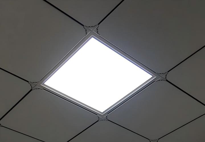
How Does Aluminum PCB Improve Thermal Performance for Large-Area LED Flood Lights?
Large-area outdoor LED flood lights produce intense heat during continuous use, and poor heat dissipation directly causes LED burnout, uneven brightness, and shorter fixture life. Unlike standard FR4 PCBs that trap heat, high-quality LED flood light aluminum PCB uses specialized materials to move heat away from critical components efficiently, ensuring steady, consistent performance in harsh outdoor conditions. Below are the key customer-focused ways our aluminum PCB boosts thermal performance for large-scale outdoor lighting:
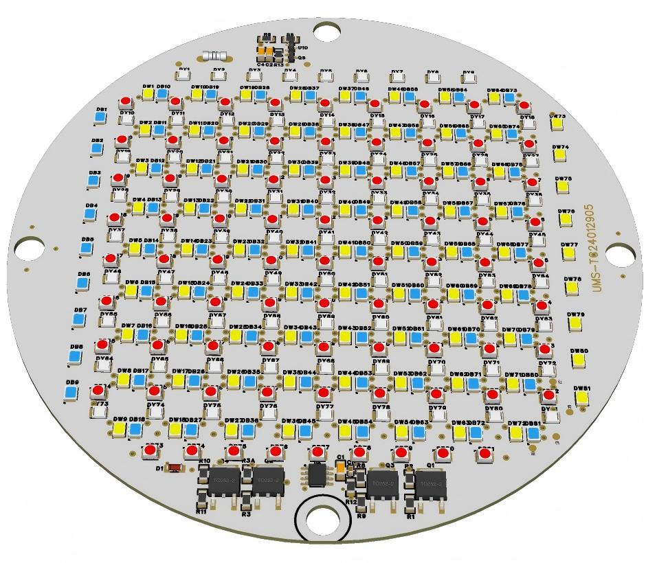
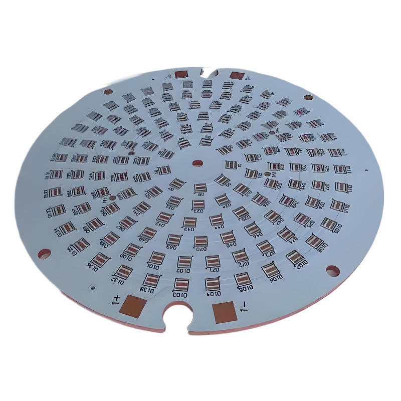
- High-conductivity aluminum base for fast heat transfer: Our aluminum PCB features a premium aluminum substrate with thermal conductivity up to 4.0 W/(m·K), far higher than standard PCBs. This base acts as a built-in heat sink, quickly pulling heat away from LED chips to prevent overheating and hotspots that damage components and dim lighting.
- Optimized thin dielectric layer for lower thermal resistance: We use a thin, high-performance dielectric layer that balances electrical insulation and minimal thermal resistance. This design removes the biggest barrier to heat flow in standard PCBs, allowing heat to pass smoothly from the LED circuit layer to the aluminum base for fast dissipation.
- Full-surface even heat distribution: The rigid aluminum base spreads heat evenly across the entire PCB surface, eliminating concentrated hotspots common with standard circuit boards. This ensures every LED on large-area flood lights operates at the same stable temperature, avoiding patchy, inconsistent lighting across wide outdoor spaces.
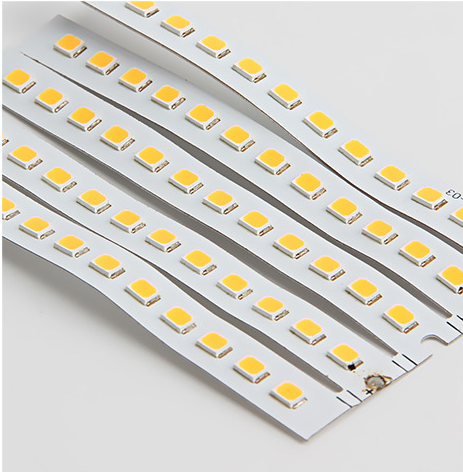
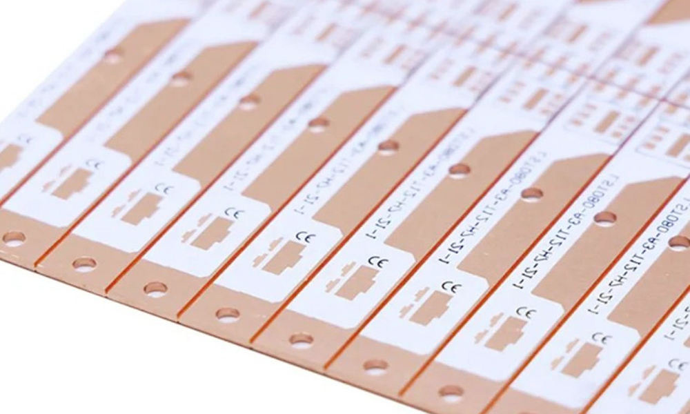
- Thick copper traces for reduced heat buildup: Our LED flood light aluminum PCB uses 2-3 oz thick copper traces that handle high-power current efficiently without generating extra heat. Thick traces lower resistance-related heat output, supporting the high power demands of large-area flood lights while keeping operating temperatures low.
- Stable thermal performance in extreme temperatures: The aluminum construction maintains consistent thermal efficiency across a wide temperature range (-40°C to 125°C), so heat dissipation stays reliable in sweltering summer heat or freezing winter conditions without performance drops.
- Seamless compatibility with external heat sinks: The flat, solid aluminum surface is designed to fit perfectly with external heat sinks or lighting fixture housings, creating a continuous heat dissipation path. This extra thermal support maximizes cooling efficiency for high-power flood lights used in large outdoor venues.
Why Do Outdoor LED Flood Lights Fail Easily Without a High-Quality Aluminum PCB?
Outdoor LED flood lights operate in unforgiving environments, facing constant high heat, moisture, and extreme temperature swings and standard FR4 PCBs simply cannot withstand these harsh conditions long-term. Without a premium LED flood light aluminum PCB, heat generated by high-power LED chips gets trapped near the components, creating dangerous hotspots that speed up LED degradation, solder joint damage, and circuit trace burnout. This trapped heat is the top cause of frequent fixture failures, sudden dimming, and complete breakdowns for outdoor flood lights running on generic PCBs.
Moisture and thermal instability make failure even more likely for non-aluminum PCB setups. Standard PCBs lack waterproof, corrosion-resistant properties and proper thermal stability, letting moisture seep into circuits to cause short circuits, while poor heat distribution leads to warping and performance decline over time. Unlike thin, low-durability standard boards, high-quality aluminum PCBs deliver consistent heat dissipation and outdoor protection, eliminating the two biggest failure triggers and keeping outdoor flood lights running reliably for far longer.
How to Choose a Waterproof Aluminum PCB for Outdoor Flood Light Applications?
Choosing the right waterproof aluminum PCB directly cuts down outdoor flood light failures, extends service life, and keeps lighting performance stable in rain, humidity, and harsh weather. Low-quality PCBs often fail to block moisture or dissipate heat properly, leading to frequent breakdowns and uneven brightness. Below are practical, customer-focused tips to select the best waterproof LED flood light aluminum PCB for your outdoor large-area lighting projects.
- Prioritize IP67-rated waterproof & sealed structure: Look for a full sealed dielectric layer and professional waterproof coating to stop moisture and rainwater from seeping in, ideal for long-term outdoor use in wet, high-humidity environments.
- Check thermal conductivity for high-power compatibility: Optimize for thermal conductivity between 2.0-4.0 W/(m·K) to handle heat from high-power flood LEDs, avoiding overheating and light decay while maintaining consistent brightness.
- Select corrosion-resistant aluminum base material: Choose anti-UV and anti-rust aluminum substrates that withstand outdoor elements like sun exposure, rain, and temperature changes, preventing material degradation over time.
- Pick reinforced thick copper traces: 2-3 oz thick copper traces ensure stable power delivery, resist damage from frequent heat expansion and contraction, and support the high load demands of large-area flood lights.
- Verify wide operating temperature tolerance: Ensure the PCB works steadily in -40°C to 125°C, so thermal and waterproof performance stays consistent in extreme cold or hot outdoor conditions.
- Choose rigorously tested products from reliable suppliers: Select PCBs that pass full reliability testing for waterproofing and heat dissipation, ensuring consistent quality and long-term outdoor durability.
What Thermal Specifications Make an Aluminum PCB Ideal for High-Power Flood Lights?
| Specification | Ideal Standard for High-Power Flood Lights |
| Thermal Conductivity | 2.0-4.0 W/(m·K) |
| Copper Foil Thickness | 2-3 oz (70-105μm) |
| Dielectric Layer Thickness | 50-100μm |
| Aluminum Base Thickness | 1.0-2.0 mm |
| Operating Temperature Range | -40°C to 125°C |
How Does Aluminum PCB Solve Uneven Heat Dissipation in Large-Scale Outdoor Lighting?
Uneven heat dissipation is one of the most common flaws in standard outdoor LED flood lights, often causing patchy brightness, color shifting, and early LED burnout across large lighting areas. Standard FR4 PCBs trap heat near LED chips and fail to spread it evenly, creating concentrated hotspots that damage internal components quickly. A high-quality LED flood light aluminum PCB fixes this issue by using the natural thermal properties of aluminum and optimized structural design to deliver consistent, uniform heat management for large-scale outdoor setups.
Unlike thin, low-conductivity standard boards, aluminum PCB acts as a full-surface heat spreader. The rigid aluminum base pulls heat away from every LED chip simultaneously and distributes it evenly across the entire panel, eliminating hotspots and temperature gaps between individual LEDs. This uniform heat distribution ensures all LEDs operate at the same stable temperature, so the flood light produces consistent brightness and color accuracy across the entire large outdoor area, with no dim or overheated sections.
EBest’s LED flood light aluminum PCB takes this performance a step further with engineered thermal pathways and low-resistance dielectric layers, which speed up heat transfer without compromising insulation. This design cuts down heat buildup in high-power outdoor applications, protects LED components from heat-related wear, and extends the overall lifespan of the lighting fixture. For large-area outdoor lighting projects, this consistent thermal control directly reduces maintenance needs and avoids costly, frequent fixture replacements.
How to Install and Maintain Aluminum PCB for Maximum Flood Light Lifespan?
Proper installation and regular maintenance are critical to unlocking the full lifespan and performance of your LED flood light aluminum PCB, especially in harsh outdoor environments. Poor installation can break thermal contact, damage waterproof seals, and cause early fixture failure, while inconsistent maintenance lets dust, moisture, and wear reduce heat dissipation efficiency over time. Following simple, professional best practices ensures your aluminum PCB stays fully functional, maintains consistent thermal performance, and extends the service life of your entire outdoor flood light system.
- Prepare a clean, flat mounting surface: Thoroughly clean the mounting area of the flood light housing to remove dust, grease, and debris. A smooth, flat surface guarantees full, even contact between the aluminum PCB and the built-in heat sink, which is essential for maximum heat transfer and preventing hotspots.
- Secure the PCB evenly with proper fasteners: Use high-quality, corrosion-resistant screws and tighten them evenly in a cross pattern to avoid warping the aluminum base. Do not over-tighten, as this can crack the dielectric layer or damage the circuit; uneven pressure also ruins heat distribution and waterproof integrity.
- Seal edges and connections for outdoor protection: Apply a thin layer of outdoor-grade, non-corrosive sealant along all PCB edges and wire entry points to boost waterproofing. This extra barrier blocks rain, humidity, and dust from penetrating the circuit, preserving both the waterproof coating and internal components long-term.
- Handle wiring carefully to avoid damage: Connect wires gently without bending or pulling the PCB traces, and double-check polarity to prevent short circuits. Use waterproof wire connectors for outdoor setups to avoid loose connections or moisture damage that can lead to fixture failure.
- Perform quarterly visual inspections: Check the aluminum PCB every three months for signs of corrosion, discoloration, loose fasteners, or moisture buildup. Pay extra attention to exposed outdoor installations, where environmental damage is more likely to occur.
- Clean gently without harsh chemicals: Wipe the PCB surface with a dry, lint-free cloth to remove dust and dirt that blocks heat dissipation. Never use acetone, abrasive cleaners, or wet chemicals, as these can damage the waterproof coating and thermal layers.
- Avoid physical stress and extreme exposure: Prevent heavy impact or bending to the aluminum PCB, and ensure the flood light housing provides proper shade from direct prolonged UV exposure when possible. This protects the board’s structural integrity and maintains consistent performance year-round.
FAQs About LED Flood Light Aluminum PCB
Q1: What is the main difference between LED flood light aluminum PCB and standard FR4 PCB for outdoor use?
A1: The main difference is thermal conductivity and outdoor durability; aluminum PCB has far superior heat dissipation and better moisture/corrosion resistance than FR4 PCB, making it suitable for harsh outdoor large-area lighting conditions.
Q2: Can EBest’s LED flood light aluminum PCB withstand heavy rain and high humidity?
A2: Yes, our aluminum PCBs come with a professional waterproof coating and sealed dielectric layers, designed to resist moisture penetration and perform reliably in heavy rain, high humidity, and damp outdoor environments.
Q3: How does aluminum PCB extend the lifespan of outdoor LED flood lights?
A3: Aluminum PCB efficiently dissipates heat away from LED chips, preventing overheating and component degradation; it also resists moisture and corrosion, reducing common failure causes and extending fixture lifespan significantly.
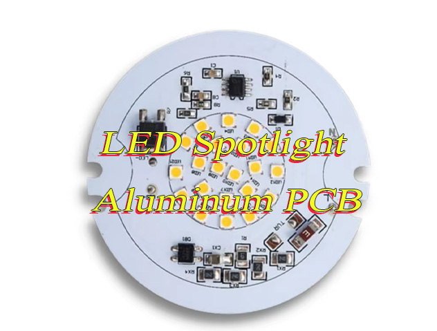
Q4: Is LED spotlight aluminum PCB compatible with large-area flood light systems?
A4: Yes, LED spotlight aluminum PCB shares the same high-thermal and durable design as our flood light aluminum PCB, and can be adapted for integrated large-area outdoor lighting systems that combine spot and flood lighting functions.
Q5: What thermal rating should I look for in an aluminum PCB for high-power outdoor flood lights?
A5: For high-power outdoor flood lights, look for an aluminum PCB with a thermal conductivity rating of 2.0-4.0 W/(m·K) and a wide operating temperature range to ensure stable thermal performance in all outdoor conditions.
Get Your Premium LED Flood Light Aluminum PCB from EBest Today
If you need high-thermal, waterproof, and durable LED flood light aluminum PCB for large-area outdoor lighting projects, EBest is your trusted partner. We specialize in manufacturing top-quality LED flood light aluminum PCB and LED spotlight aluminum PCB solutions that meet the strictest industry standards for outdoor performance. Place your order with us today by contacting our team at sales@bestpcbs.com, and let us provide you with reliable PCB products that eliminate outdoor lighting failures and boost your project’s long-term performance.