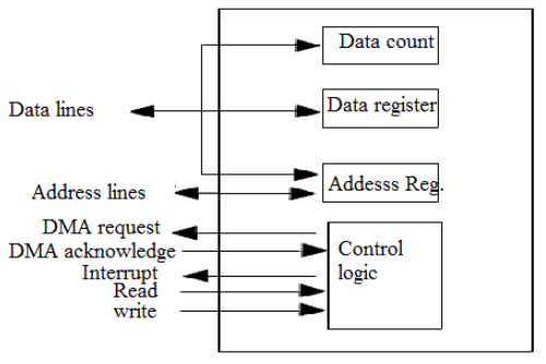
PCB manufacturing PCB manufacturing
Home > Blog

IATF 16949 Certified PCB Supplier: What Automotive Buyers Must Know

December 16th, 2025

An IATF 16949 certified PCB supplier is a manufacturer approved to produce automotive PCBs under strict quality, traceability, and risk-control systems required by global OEMs.

This certification confirms that PCB processes are controlled, repeatable, and audited for defect prevention rather than post-inspection.

For automotive buyers, choosing an IATF 16949 certified PCB supplier directly reduces recall risk, audit pressure, and long-term field failures.

What Is an IATF 16949 Certified PCB Supplier?

An IATF 16949 certified PCB supplier is a PCB manufacturer that complies with the global automotive quality management standard issued by the International Automotive Task Force.

This standard requires:

  • Full process traceability
  • Preventive quality planning (APQP, FMEA)
  • Continuous improvement and corrective action systems
  • Controlled production from prototype to mass volume

Unlike general certifications, IATF 16949 applies only to automotive supply chains.

IATF 16949 Certified PCB Supplier: What Automotive Buyers Must Know

What Is an IATF 16949 Certified PCB Supplier?

Why Do Automotive OEMs Require IATF 16949 PCB Suppliers?

Automotive OEMs require IATF 16949 because PCB failures can trigger recalls, safety risks, and regulatory penalties.

This certification ensures:

  • Stable PCB manufacturing processes
  • Early risk identification
  • Consistent quality across production lots
  • Audit-ready documentation for OEM and Tier-1 reviews

For safety-critical electronics, uncertified suppliers introduce unacceptable risk.

Which Automotive PCBs Must Come from an IATF 16949 Certified Factory?

Automotive PCBs that typically require IATF 16949 certification include:

  • Engine control units (ECU)
  • ADAS and camera modules
  • Radar and RF automotive PCBs
  • Battery management systems (BMS)
  • Power inverter and motor control boards
  • Safety and braking control electronics

If a PCB affects vehicle safety, emissions, or power control, certification is expected.

IATF 16949 vs ISO 9001 for PCB Manufacturing

ISO 9001 focuses on general quality procedures across industries. IATF 16949 focuses on automotive risk prevention and process stability.

Key differences for PCB buyers:

  • IATF 16949 requires FMEA and PPAP
  • ISO 9001 allows broader process variation
  • IATF 16949 enforces corrective action with data
  • ISO 9001 emphasizes documentation, not automotive reliability

ISO 9001 alone is not sufficient for automotive PCBs.

IATF 16949 vs ISO 9001 for PCB Manufacturing

Core Capabilities Required from an IATF 16949 PCB Supplier

An automotive-qualified PCB supplier must demonstrate both engineering and process discipline.

This includes impedance-controlled stackups, material consistency, SPC monitoring, and documented change control.

Below is a technical capability table automotive buyers often request.

Capability CategoryAutomotive PCB RequirementTypical Specification Range
PCB Layer CountMultilayer & HDI2–20 layers
Controlled ImpedanceMandatory for high-speed / RF±5% to ±10%
Copper ThicknessPower and signal balance0.5–6 oz
Minimum Trace / SpaceDense automotive layouts3/3 mil
Via TechnologyReliability under vibrationThrough, blind, buried, microvia
Laminate MaterialsThermal and electrical stabilityHigh-Tg FR-4, Rogers, hybrid stackups
Surface FinishAutomotive solderabilityENIG, ENEPIG, OSP
Operating TemperatureHarsh environment tolerance−40°C to +125°C
Traceability SystemMandatory under IATF 16949Lot-level MES tracking
Quality DocumentationOEM audit compliancePPAP, FMEA, Control Plan, SPC
Production VolumePrototype to mass productionNPI → high volume
Reliability TestingAutomotive qualificationThermal cycling, cross-section

How Traceability Works in IATF 16949 PCB Manufacturing?

In IATF 16949 certified PCB manufacturing, traceability links each PCB lot to materials, processes, inspections, and operators.

Traceability systems typically record:

  • Laminate batch numbers
  • Inner layer imaging data
  • Lamination cycles
  • Plating and surface finish parameters
  • Final inspection results

This allows fast containment if field issues occur.

What Quality Risks Exist Without an IATF 16949 PCB Supplier?

Choosing a non-certified PCB supplier increases:

  • Process variation
  • Incomplete documentation
  • Poor root-cause analysis
  • Audit failures during OEM reviews

These risks often surface only after volume production begins.

What Quality Risks Exist Without an IATF 16949 PCB Supplier?

What Documents Should an IATF 16949 PCB Supplier Provide?

Automotive buyers should expect:

  • PPAP documentation
  • PFMEA and Control Plans
  • Material certifications
  • SPC and inspection reports
  • Change management records

Missing documents usually indicate limited automotive readiness.

Prototype vs Mass Production: What Buyers Often Overlook

IATF 16949 applies from the prototype stage, not only mass production.

Controlled materials, documented changes, and engineering approvals must begin early.
Skipping these steps creates instability during ramp-up.

Automotive-ready PCB suppliers treat prototypes as production-intent builds.

Why Automotive Buyers Choose EBest Circuit (Best Technology) as Their IATF 16949 Certified PCB Supplier?

EBest Circuit (Best Technology) supports automotive PCB projects under IATF 16949, ISO 9001, and ISO 13485, AS9100D systems.

Our company delivers:

  • Automotive-grade multilayer and HDI PCBs
  • Controlled impedance and high-frequency designs
  • MES-based traceability
  • Structured documentation for OEM audits
  • Smooth transition from prototype to mass production

This combination reduces buyer risk and accelerates project approval.

FAQs

1. Is IATF 16949 mandatory for automotive PCBs?

    Yes, for OEM and safety-critical automotive electronics.

    2. Does IATF 16949 cover PCB prototypes?

    Yes. Process control applies from early builds.

    3. Can ISO 9001 replace IATF 16949?

    No. ISO 9001 alone does not meet automotive standards.

    4. How can buyers verify IATF 16949 certification?

    Check the certificate scope, issuing body, and audit validity.

    5. Why is traceability critical in automotive PCBs?

    It enables fast containment and root-cause analysis during failures.

    IATF 16949 Certified PCB Supplier: Automotive-Grade PCBs You Can Trust

    December 16th, 2025

    Selecting an IATF 16949 certified PCB supplier is not just a purchasing decision—it is a risk management strategy for automotive electronics. With vehicles increasingly dependent on electronics for safety, performance, and connectivity, PCB quality directly impacts system reliability and brand reputation.

    This in-depth guide explains what IATF 16949 certification means for PCB manufacturing, how it affects automotive applications, how to evaluate certified suppliers, and why EBest Circuit (Best Technology) is a trusted partner for automotive PCB projects.

    What Is an IATF 16949 Certified PCB?

    An IATF 16949 certified PCB is a printed circuit board manufactured under a quality management system that complies with IATF 16949, the global automotive industry standard that replaced ISO/TS 16949.

    Unlike general ISO 9001 certification, IATF 16949 is automotive-specific and focuses on:

    • Defect prevention rather than detection
    • Risk-based process control
    • Continuous improvement throughout the supply chain
    • Traceability and accountability at every manufacturing stage

    For PCB manufacturing, this means every process—from laminate sourcing and copper plating to imaging, drilling, surface finish, and final inspection—is documented, controlled, audited, and continuously improved.

    An IATF 16949 certified PCB supplier is qualified to support automotive OEMs, Tier 1 suppliers, and Tier 2 suppliers globally.

    IATF 16949 Certified PCB Supplier: Automotive-Grade PCBs You Can Trust https://www.bestpcbs.com/blog/2025/12/iatf-16949-certified-pcb-supplier/

    Typical Applications for IATF 16949 Certified PCBs

    Automotive electronics operate in environments that are far more demanding than consumer or industrial electronics. As a result, IATF 16949 certified PCBs are widely used in systems where failure is unacceptable, like:

    • Electric vehicle (EV) systems – BMS, OBC, inverters, DC-DC converters
    • ADAS & autonomous driving modules – radar, camera, LiDAR control boards
    • Powertrain & engine control units (ECU)
    • Infotainment and cockpit electronics
    • Body electronics – lighting control, window and seat modules
    • Chassis and safety systems – ABS, EPS, airbag controllers

    These applications demand high reliability, thermal stability, and long service life, often exceeding 10–15 years.

    Why IATF 16949 Certification Is Critical in Automotive Electronics?

    Automotive PCBs must survive:

    • Temperature ranges from -40°C to +125°C or higher
    • Continuous vibration and mechanical shock
    • Long-term exposure to humidity, oils, and chemicals
    • 10–20 years of operational life

    IATF 16949 certification ensures that a PCB supplier has systems in place to manage these risks through:

    • APQP (Advanced Product Quality Planning) for new product introduction
    • FMEA (Failure Mode and Effects Analysis) to identify and mitigate risks
    • SPC (Statistical Process Control) to maintain consistency
    • Root cause analysis and corrective actions (8D, PDCA)
    • Supplier quality management for raw materials

    Without IATF 16949, PCB quality may rely too heavily on final inspection rather than process stability, which is unacceptable for automotive use.

    Why IATF 16949 Certification Is Critical in Automotive Electronics?  https://www.bestpcbs.com/blog/2025/12/iatf-16949-certified-pcb-supplier/

    Does IATF 16949 Mean Zero Defects?

    No quality standard can guarantee absolute zero defects—but IATF 16949 is designed to make defects rare, predictable, and preventable. Instead of reacting to failures, IATF 16949 requires:

    • Early risk identification
    • Process capability monitoring
    • Immediate corrective action when trends appear
    • Continuous reduction of variation

    In practice, this leads to dramatically lower defect rates, improved field reliability, and reduced recall risk for automotive customers.

    Does IATF Certification Automatically Mean Automotive Capability?

    No, not always. IATF 16949 certifies the quality management system, not the technical capability alone.

    A truly automotive-capable IATF 16949 certified PCB supplier must also demonstrate:

    • Experience with automotive-grade laminates (high Tg, low CTE, CAF-resistant)
    • Tight control of dielectric thickness and impedance
    • Stable copper plating and via reliability
    • High-reliability surface finishes (ENIG, ENEPIG, Immersion Silver)
    • Proven performance in thermal cycling and reliability testing

    Certification plus real automotive project experience is the key.

    What Makes an IATF 16949 Certified PCB Manufacturer Different?

    Compared to standard PCB manufacturers, IATF 16949 certified suppliers offer:

    • Full lot and serial traceability
    • Controlled change management (ECN & PCN)
    • PPAP documentation upon request
    • Automotive-focused process audits
    • Long-term supply consistency

    These differences are essential for OEMs who cannot afford field failures or recalls.

    What Makes an IATF 16949 Certified PCB Manufacturer Different? https://www.bestpcbs.com/blog/2025/12/iatf-16949-certified-pcb-supplier/

    How to Verify an IATF 16949 Certified PCB Supplier?

    Before selecting a supplier, always verify:

    1. Valid IATF 16949 certificate (issued by an accredited certification body)
    2. Certificate scope explicitly covering PCB manufacturing
    3. Evidence of automotive project experience
    4. Ability to provide PPAP, FMEA, control plans, and traceability records
    5. Clear change management and corrective action procedures

    A professional IATF 16949 certified PCB supplier will proactively provide this information.

    EBest Circuit (Best Technology) – Your Reliable IATF 16949 Certified PCB Supplier

    EBest Circuit (Best Technology) is a trusted IATF 16949 certified PCB supplier, supporting automotive electronics manufacturers with stable quality, engineering expertise, and long-term production reliability.

    At EBest Circuit (Best Technology), our automotive PCBs are manufactured under a fully implemented IATF 16949 quality management system, ensuring process stability, traceability, and long-term reliability for safety-critical automotive electronics.

    Our Automotive PCB Manufacturing Capability

    CategoryCapability Details
    CertificationIATF 16949 (Automotive Quality Management System)
    PCB TypesSingle-sided, Double-sided, Multilayer Automotive PCBs
    Layer Count1–20+ layers (automotive control & power applications)
    Base MaterialsFR-4 (High Tg), Low-loss laminates, Automotive-grade materials
    Tg Range≥170°C (automotive and high-reliability requirements)
    Board Thickness0.4 mm – 3.2 mm (custom thickness available)
    Copper Thickness0.5 oz – 6 oz (inner & outer layers)
    Heavy Copper PCBUp to 6 oz for EV power electronics
    Min Line / Space4 / 4 mil (HDI options available)
    Min Hole Size0.20 mm (laser vias for HDI upon request)
    Aspect RatioUp to 10:1
    Impedance Control±5% tolerance (automotive signal integrity requirements)
    Surface FinishesENIG, ENEPIG, Immersion Silver, Immersion Tin, OSP
    Solder MaskAutomotive-grade epoxy, green / black / red (others on request)
    SilkscreenWhite, yellow (high contrast for traceability)
    Panel SizeUp to 600 × 1200 mm
    CAF ResistanceCAF-resistant material selection & process control
    Thermal ReliabilityDesigned for −40°C to +125°C operating environments
    Electrical TestingFlying Probe Test, Fixture E-Test (100% testing)
    InspectionAOI, X-ray (for HDI & fine-pitch designs)
    Reliability TestingThermal shock, thermal cycling (upon request)
    TraceabilityFull lot & material traceability per IATF 16949
    Documentation SupportPPAP, Control Plan, PFMEA, SPC records

    Our Services for IATF 16949 Certified PCB Projects

    We provide comprehensive support throughout the product lifecycle:

    • Automotive PCB DFM and engineering review
    • Prototype, NPI, and mass production support
    • PPAP and quality documentation assistance
    • Long-term supply and lifecycle management
    • PCB & PCBA one-stop manufacturing solutions

    Our goal is to help customers reduce risk, shorten development cycles, and scale confidently. If you’re searching for a dependable iatf 16949 certified pcb supplier, EBest Circuit (Best Technology) is ready to support your automotive electronics projects.

    Frequently Asked Questions (FAQ)

    1. Is IATF 16949 mandatory for automotive PCBs?

      Most automotive OEMs and Tier 1 suppliers require IATF 16949 certification for PCB suppliers.

      2. Can IATF 16949 certified suppliers support EV and ADAS projects?

      Yes. IATF 16949 is widely adopted in EV, hybrid, and autonomous vehicle electronics.

      3. Does IATF 16949 cover PCB assembly?

      Only if PCBA is included in the certification scope. Always verify the certificate details.

      4. How often is IATF 16949 audited?

      Certified suppliers undergo annual surveillance audits and full recertification every three years.

      Why Does Yellow Discoloration Appear on Al₂O₃ DBC Substrates?

      December 16th, 2025

      Yellow discoloration on Al₂O₃ DBC substrates layers is occasionally observed after DBC bonding. For many engineers, this visual change raises a practical question: does ceramic yellowing indicate a performance risk? Why does it become yellow? This article explains the material mechanisms behind discoloration, and why it does not compromise DBC substrate reliability.

      What Is an Al₂O₃ DBC Substrate?

      An Al₂O₃ DBC (Direct Bonded Copper) substrate is a ceramic metal composite formed by directly bonding copper foil to an alumina ceramic plate under high temperature and controlled oxygen atmosphere.

      This structure is widely used in power modules, inverters, IGBT packages, and automotive electronics, where thermal conductivity and electrical insulation are critical. The bonding process relies on interfacial chemical reactions, not adhesives.

      What Is an Al₂O₃ DBC Substrate? https://www.bestpcbs.com/blog/2025/12/why-does-yellow-discoloration-appear-on-al₂o₃-dbc-substrates/

      How Does the DBC Bonding Process Work?

      During DBC sintering, copper and alumina interact through a thermally activated oxidation-reduction mechanism.

      At elevated temperatures and controlled oxygen levels:

      • Copper surface oxidizes to form a thin Cu₂O layer
      • When the temperature exceeds the eutectic point, a Cu–Cu₂O eutectic liquid phase forms
      • This liquid phase wets both copper and Al₂O₃ surfaces effectively
      • Copper oxide reacts with alumina to form CuAlO₂

      The reaction can be summarized as:

      Cu₂O + Al₂O→ CuAlO

      How Does the DBC Bonding Process Work?https://www.bestpcbs.com/blog/2025/12/why-does-yellow-discoloration-appear-on-al₂o₃-dbc-substrates/

      CuAlO₂ acts as a ceramic-like bonding phase, enabling strong metallurgical adhesion between copper and ceramic.

      What Is the Bonding Layer Made Of?

      After bonding, a thin interfacial layer composed mainly of CuAlO exists between copper and Al₂O₃.

      Key characteristics of this layer:

      • Ceramic oxide with dark red to yellowish color
      • Excellent resistance to acids and alkalis
      • Difficult to remove completely using standard copper etching chemicals
      What Is the Bonding Layer Made Of?https://www.bestpcbs.com/blog/2025/12/why-does-yellow-discoloration-appear-on-al₂o₃-dbc-substrates/

      When surface copper is etched away, the bonded ceramic area often appears more yellow than unbonded areas. This visual difference directly relates to the presence of the bonding layer.

      Why Does Yellow Discoloration Appear on the Ceramic Surface?

      Yellowing originates from two simultaneous material phenomena, both occurring during high-temperature DBC sintering.

      1. Influence of the CuAlO₂ Bonding Layer

      CuAlO₂ itself has a reddish-yellow ceramic appearance. Because this compound forms through interfacial reactions, its thickness is not perfectly uniform across the substrate.

      Even nanometer-level thickness variation can lead to visible color differences after copper removal.

      Why Does Yellow Discoloration Appear on the Ceramic Surface?https://www.bestpcbs.com/blog/2025/12/why-does-yellow-discoloration-appear-on-al₂o₃-dbc-substrates/

      2. Migration of Ceramic Sintering Additives

      Most industrial Al₂O₃ ceramics used for DBC are 96% alumina, not 100% pure.

      They contain small amounts of sintering additives such as:

      • SiO₂
      • CaO
      • MgO

      These additives improve ceramic densification during firing.

      During DBC bonding:

      • High temperatures cause partial diffusion of these additives toward the surface
      • EDX analysis shows increased Si, Ca, and Mg content in yellowed areas
      • Higher surface concentration of these oxides correlates with yellow coloration

      This behavior is consistent with ceramic sintering literature, which confirms that increased SiO₂ content can cause alumina yellowing.

      How Does the DBC Bonding Process Create a Strong Interface?

      DBC bonding relies on controlled oxidation and eutectic reactions at high temperature.

      During sintering:

      • Copper forms a thin Cu₂O layer under controlled oxygen content
      • Above the eutectic temperature, a Cu–Cu₂O liquid phase appears
      • This liquid wets both copper and Al₂O₃ surfaces
      • Interfacial reactions form CuAlO₂, enabling direct bonding

      This mechanism creates a chemically bonded interface, which is critical for long-term thermal cycling stability.

      Why Is the Yellow Color Often Non-Uniform?

      The discoloration is rarely perfectly even. This non-uniformity comes from reaction uncertainty, not process instability.

      Key reasons include:

      • CuAlO₂ formation varies slightly across the bonding interface
      • Sintering additive diffusion is not perfectly uniform at the micro-scale
      • Both effects occur at nanometer-level thickness differences

      Even minor variations become visible on ceramic surfaces due to light reflection and oxide color sensitivity.

      Does Yellow Discoloration Affect DBC Substrate Performance?

      This is the most important question for engineers and customers. Extensive testing was performed on:

      • DBC substrates with severe yellow discoloration
      • DBC substrates with minimal or no discoloration

      The results show:

      • No meaningful difference in electrical insulation
      • No degradation in thermal performance
      • No impact on mechanical bonding strength
      • No reliability concerns in functional testing

      In short, yellow discoloration is a cosmetic phenomenon, not a functional defect.

      Does Yellow Discoloration Affect DBC Substrate Performance? https://www.bestpcbs.com/blog/2025/12/why-does-yellow-discoloration-appear-on-al₂o₃-dbc-substrates/

      What Is an Al₂O₃ DBC Substrate Used For?

      Al₂O₃ DBC substrates are widely applied in:

      • IGBT and power module packaging
      • Automotive inverters and motor drives
      • Industrial power supplies
      • Renewable energy systems

      Their value lies in a balanced combination of electrical insulation, thermal conduction, and mechanical stability. The copper–ceramic interface is formed through a metallurgical bonding process rather than adhesives or plating.

      How EBest Circuit (Best Technology) Controls DBC Substrate Quality?

      At EBest Circuit (Best Technology), DBC substrates are produced with strict control over:

      • Oxygen concentration during bonding
      • Temperature uniformity across furnaces
      • Ceramic material composition and sourcing
      • Post-bonding inspection and testing

      Our engineering team evaluates DBC substrates based on measurable electrical and thermal performance, not cosmetic appearance alone.

      This approach ensures stable results for:

      • Automotive-grade power electronics
      • Industrial and renewable energy systems
      • High-reliability inverter applications

      Conclusion

      Yellow discoloration on Al₂O₃ DBC substrates originates from:

      • CuAlO₂ formation at the bonding interface
      • Surface diffusion of ceramic sintering additives

      Both effects occur during normal DBC sintering and may vary slightly across the substrate.
      Extensive testing confirms that this discoloration does not affect DBC performance or reliability.

      For power electronics applications, engineering performance matters far more than visual color uniformity.

      What Is 3.2mm to Inches in Engineering and Manufacturing?

      December 16th, 2025

      3.2mm to inches equals 0.12598 inches, commonly rounded to 0.126 inches.

      lthough 3.2mm is often associated with 1/8 inch, it is slightly larger than 1/8″ (which equals 3.175mm). For general PCB fabrication, hardware selection, and sheet material, treating 3.2mm as ≈ 1/8 inch is acceptable. For tight-tolerance or mating components, always use the exact value: 0.12598 inches.

      This conversion is frequently referenced in PCB thickness control, mechanical part matching, and cross-standard manufacturing, especially when metric-designed components are produced or assembled in imperial-based environments.

      What Is 3.2mm to Inches in Engineering and Manufacturing?  https://www.bestpcbs.com/blog/2025/12/what-is-3-2mm-to-inches-in-engineering-and-manufacturing/

      Engineering Method for Converting 3.2mm to Inches

      All engineering-grade conversions rely on a fixed constant.

      1 inch = 25.4 millimeters (exact, not approximate)

      To convert millimeters to inches:

      3.2 ÷ 25.4 = 0.12598 inches

      In CAD systems, CAM outputs, and inspection reports, engineers usually keep four to five decimal places to prevent cumulative dimensional deviation. Rounding is applied only at the documentation or purchasing stage.

      Why 3.2mm Is Widely Used in PCB and Mechanical Manufacturing?

      3.2mm is considered a hybrid-standard thickness. It bridges metric design logic with imperial production habits.

      In PCB manufacturing, 3.2mm is commonly selected for:

      • Power distribution boards
      • Backplanes and structural PCBs
      • Boards used as mounting or support elements
      • Industrial controller PCBs requiring stiffness

      In mechanical manufacturing, 3.2mm sheet thickness is frequently used for:

      • Aluminum and steel brackets
      • Equipment enclosures
      • Protective covers and panels

      This thickness offers good rigidity while remaining compatible with standard drilling, routing, and bending processes.

      Why 3.2mm Is Widely Used in PCB and Mechanical Manufacturing? https://www.bestpcbs.com/blog/2025/12/what-is-3-2mm-to-inches-in-engineering-and-manufacturing/

      3.2mm to Inches Chart ((Fractional & Decimal)

      The table below shows 3.2mm to inches alongside nearby metric sizes, including fractional inch equivalents commonly used in hardware, PCB thickness, and metal stock selection.

      Millimeters (mm)Fractional InchesDecimal Inches
      2.0 mm5/64″0.0787″
      2.4 mm3/32″0.0937″
      3.2 mm≈ 1/8″0.12598″ (≈ 0.126″)
      3.5 mm9/64″0.1378″
      4.0 mm5/32″0.1575″
      4.8 mm3/16″0.1890″
      6.4 mm1/4″0.2520″

      Engineering note:

      1/8 inch equals 3.175mm, not 3.2mm. The 0.025mm difference may matter in precision machining, PCB slot sizing, or press-fit applications.

      Why 3.2mm Is Commonly Treated as 1/8 Inch?

      In practice, 3.2mm is widely treated as a nominal 1/8-inch equivalent because:

      • The dimensional difference is very small
      • Standard drill bits and tooling align closely
      • PCB thickness tolerances usually exceed ±0.025mm
      • Hardware and sheet stock are often sold by nominal size

      This is why datasheets, BOMs, and supplier listings frequently group 3.2mm and 1/8 inch together.

      3.2mm to cm in Technical Documentation

      3.2mm equals 0.32 cm.

      This conversion is exact and does not involve rounding. It is often used in:

      • Engineering specifications
      • International standards
      • Educational and training materials

      Centimeter notation is common in documentation intended for non-manufacturing audiences.

      3.2mm to Feet in Industrial Context

      3.2mm equals 0.0105 feet.

      While feet are rarely used for small dimensions, this conversion may appear in:

      • Mixed-unit architectural layouts
      • Legacy documentation
      • Facility-level mechanical references

      For fabrication work, inches or millimeters remain preferred.

      Is 3.2mm the Same as 1/8 Inch in PCB and Mechanical Design?

      No. 1/8 inch equals 3.175mm, not 3.2mm.

      The difference is 0.025mm, which may seem negligible but can impact:

      • PCB edge connector fit
      • Slot and cutout tolerances
      • Press-fit components
      • Stack-up alignment in assemblies

      In high-reliability PCB designs, this difference must be evaluated rather than assumed acceptable.

      Practical PCB Applications of 3.2mm Thickness

      In PCB fabrication, 3.2mm thickness is often chosen when mechanical strength is more important than weight reduction.

      Typical PCB use cases include:

      • High-current power boards
      • Backplanes in industrial systems
      • PCBs acting as mechanical supports
      • Boards exposed to vibration or shock

      Thicker boards reduce flexing, which helps protect solder joints and large components.

      Manufacturing Implications of 3.2mm Thickness

      From a production perspective, 3.2mm thickness affects multiple processes:

      • Drilling requires adjusted feed rates
      • Routing needs deeper cut passes
      • Plating thickness becomes more critical
      • Panel warpage control becomes more important

      Manufacturers often adjust tooling and process parameters specifically for boards or parts at this thickness.

      Manufacturing Implications of 3.2mm Thickness https://www.bestpcbs.com/blog/2025/12/what-is-3-2mm-to-inches-in-engineering-and-manufacturing/

      Metric vs Imperial Units in Global PCB Manufacturing

      Most PCB designs originate in metric units. However, many:

      • Assembly fixtures
      • Test equipment
      • Mechanical interfaces

      still follow imperial standards.

      This creates frequent conversion scenarios where 3.2mm to inches must be clearly defined to avoid misinterpretation between design, fabrication, and assembly teams.

      Common Engineering Errors When Converting 3.2mm to Inches

      Errors often occur when:

      • Designers assume 3.2mm equals 1/8 inch
      • Finished thickness is confused with core thickness
      • Copper weight and surface finish are ignored
      • Units are converted without tolerance context

      These mistakes can lead to fit issues, assembly delays, or rejected parts.

      FAQs About 3.2mm to Inches

      1. How many inches is 3.2mm?

      3.2mm equals 0.12598 inches, which is commonly rounded to 0.126 inches for practical use. This value is widely accepted in engineering, PCB manufacturing, and hardware selection.

      2. Is 3.2mm the same as 1/8 inch?

      No. 3.2mm is slightly larger than 1/8 inch.

      1/8 inch equals 3.175mm, while 3.2mm equals 0.12598 inches. The difference is small but can matter in precision applications.

      3. Why is 3.2mm often called 1/8 inch?

      3.2mm is often treated as 1/8 inch because the dimensional difference is minimal and usually falls within standard manufacturing tolerances. Many suppliers group these sizes together for convenience.

      4. Is 3.2mm a standard PCB thickness?

      Yes. 3.2mm is a common PCB thickness, especially for power boards, backplanes, and mechanically reinforced PCBs. It provides higher rigidity compared to thinner boards.

      5. Can 3.2mm replace 1/8 inch material?

      In most cases, yes.

      For sheet metal, PCB panels, and brackets, 3.2mm can replace 1/8 inch. Always verify tolerance requirements for mating or press-fit parts.

      6. What is the formula to convert 3.2mm to inches?

      The formula is:

      Inches = millimeters ÷ 25.4

      3.2 ÷ 25.4 = 0.12598 inches

      7. Does PCB copper thickness affect the final 3.2mm board thickness?

      Yes. The finished PCB thickness includes laminate, copper layers, and surface finish. Copper weight and plating can slightly increase the final thickness beyond the nominal 3.2mm.

      What are PCB layers? PCB layers explained

      December 15th, 2025

      PCB layers are the physical and electrical building blocks of a printed circuit board. It is a layered structure made by stacking copper and insulating materials together. Each layer serves a clear purpose, such as carrying signals, distributing power, or providing a stable ground reference. The way these layers are arranged directly affects how the board performs.

      What are PCB layers? PCB layers explained

      What are layers on a PCB?

      A PCB is not just a flat sheet. It is a carefully stacked structure. Each layer has a clear job. Together, these layers allow electricity to flow in a controlled way.

      At the most basic level, a PCB layer can be copper, insulation, or surface coating. Copper layers carry signals and power. Insulation layers keep signals apart. Surface layers protect the board and make assembly possible.

      PCB board layers define how complex a board can be. A simple product may need only two layers. A high-speed device may need many more. Each added layer increases routing space. It also improves signal control.

      The layers of a PCB are planned during design. Engineers decide how many layers are needed. They also decide what each layer will do. This plan is called a PCB layer stackup.

      Understanding PCB layers meaning helps avoid design mistakes. It also helps control cost. Too many layers waste money. Too few layers cause noise and routing problems.

      At EBest Circuit (Best Technology), PCB layers design is part of our turnkey EMS service. From layout to final assembly, layer planning is handled early. This reduces risk and shortens lead time.

      How are PCB layers produced?

      PCB layers are produced through a precise and repeatable process. Each step matters. Small errors can affect the entire board.

      • The process starts with copper-clad laminate. This material has copper bonded to fiberglass. The fiberglass is usually FR-4. It offers strength and heat resistance.
      • For inner layers, copper is first etched. A photo image defines the circuit pattern. Chemicals remove unwanted copper. What remains forms the traces.
      • After etching, inner layers are inspected. Alignment is checked. Shorts and opens are detected early.
      • Next comes lamination. Multiple etched layers are stacked together. Prepreg sheets are placed between them. Heat and pressure bond everything into one board.
      • Once laminated, holes are drilled. These holes connect different PCB copper layers. Copper plating coats the hole walls. This creates electrical paths between layers.
      • Outer layers are then formed. The same imaging and etching steps apply. Finally, solder mask and surface finish are added.
      What are PCB layers? PCB layers explained

      Throughout this process, PCB layers stack up accuracy is critical. Even slight shifts can cause failures. At EBest Circuit (Best Technology), automated inspection ensures layer alignment stays within tight limits. Because we control both PCB fabrication and assembly, feedback is fast. That is a key benefit of turnkey EMS services.

      What does a 2 layer PCB mean?

      A 2 layer PCB is the most common board type. It has copper on the top and bottom. Between them is an insulating core.

      In a PCB 2 layers design, components usually sit on the top. Traces run on both sides. Vias connect the two copper layers. This structure is easy to understand. It is also cost-effective. That is why many consumer products use it.

      However, routing space is limited. Power and signal traces share the same layers. This can cause noise in sensitive circuits. Still, for low-speed designs, a two-layer board works well. Simple power supplies often use this type. Basic controllers also fit well.

      At EBest Circuit (Best Technology), we manufacture high-quality two-layer boards at scale. Even simple boards benefit from good material and process control.

      What does a 4 layer PCB mean?

      A 4 layer PCB adds two inner copper layers. This design offers more control and flexibility. It is common in modern electronics.

      A typical 4 layers PCB stackup includes:

      • Top signal layer
      • Inner ground layer
      • Inner power layer
      • Bottom signal layer

      This structure separates signals from power. It also reduces noise. Signals return through a solid ground plane. A PCB 4 layers design allows shorter traces. It improves impedance control. This matters for fast digital signals.

      What are PCB layers? PCB layers explained

      In a 4 layers PCB, routing becomes cleaner. Components have more placement freedom. EMI issues are easier to manage. Cost is higher than two layers. Performance is much better.

      At EBest Circuit (Best Technology), four-layer boards are a common request. They fit well in industrial control and communication products.

      Do PCB layers matter?

      Yes, PCB layers matter a lot. They affect performance, reliability, and cost. More layers provide better signal integrity. They allow clean power distribution. They also reduce electromagnetic interference.

      • Layer count affects thermal behavior. Inner planes help spread heat. This protects sensitive components.
      • PCB layers also affect manufacturing yield. Complex stackups need tighter control. That is why experience matters.

      Choosing the wrong number of layers can cause redesigns. Redesigns cost time and money. At EBest Circuit (Best Technology), engineers review layer decisions early. This avoids later issues. It is part of our turnkey EMS approach.

      How to identify PCB layers?

      Identifying PCB layers depends on tools and experience. There are several common methods.

      • The simplest method is visual inspection. You can see top and bottom layers. Inner layers are hidden.
      • X-ray inspection reveals internal structure. It shows copper planes and vias. This is common in quality labs.
      • Another method is cross-section analysis. A small sample is cut and polished. Layers become visible under a microscope.
      • Design files also tell the story. Gerber files define each layer. The PCB layers name is listed clearly.

      At EBest Circuit (Best Technology), every board includes a clear stackup record. This supports traceability and quality control.

      Why do PCBs have multiple layers?

      PCBs have multiple layers to solve real problems. Modern electronics demand more from smaller spaces.

      More layers mean more routing room. Traces do not have to cross. This simplifies layout. Multiple layers also improve signal quality. Ground planes provide stable reference paths. Power planes deliver clean voltage. They reduce ripple and noise.

      High-density designs require many connections. Multiple layers make this possible without enlarging the board.

      In advanced devices, safety also matters. Separate layers help isolate sensitive signals. PCB design layers work together as a system. Each layer supports the others.

      How many layers can a PCB have?

      The number of PCB layers varies widely. Two layers are common. Four layers are standard for many products.

      High-end boards may have eight, twelve, or more layers. Some specialized designs go even higher. The PCB maximum layers depend on manufacturer capability. Material choice also matters.

      The PCB with most layers is usually found in servers or networking equipment. These boards handle high-speed signals and power. More layers increase cost. They also increase build time. That is why layer count should match real needs.

      At EBest Circuit (Best Technology), we can manufacture PCBs with up to 32 layers. This supports complex industrial and communication systems.

      How to decide PCB layer?

      Deciding PCB layer count starts with function. What does the product do? How fast are the signals?

      • Power requirements come next. High current often needs dedicated planes.
      • Size constraints matter. A smaller board often needs more layers.
      • Cost targets guide decisions. Each extra layer adds expense.
      • Reliability goals also influence the choice. Stable designs often use more layers.
      What are PCB layers? PCB layers explained

      At EBest Circuit (Best Technology), we assist during this stage. Our team reviews design goals. We suggest practical stackups.

      Conclusion:

      PCB layers define how a circuit board works inside. From simple two-layer boards to complex multi-layer designs, each layer has a purpose. Choosing the right PCB layers improves signal quality, reliability, and cost control.

      For technical support or project inquiries, contact us at sales@bestpcbs.com

      What Are Circuit Card Assemblies? Printed Circuit Board Assembly

      December 15th, 2025

      Circuit card assemblies sit at the core of modern electronics. A circuit card assembly is a printed circuit board that has been fully populated with electronic components and soldered into place. Once assembled, it becomes a working unit capable of controlling power, processing signals, and enabling communication within an electronic device.

      What Are Circuit Card Assemblies? Printed Circuit Board Assembly

      What Is a Circuit Card Assembly?

      A circuit card assembly, often shortened to CCA, is a printed circuit board that has electronic components mounted and connected to it. These components are not loose. They are fixed, soldered, and electrically linked according to a design.

      The circuit card assembly definition focuses on function. It is not just a board with copper paths. It is a working electronic unit. Once assembled, it can process signals, control power, or manage data.

      Many people use the term printed circuit board assembly in the same way. In daily use, they often mean the same thing. Still, some industries prefer “circuit card assembly” because it highlights the complete, functional state.

      A bare board cannot do anything alone. A circuit card assembly can. This is why CCAs are central to electronics manufacturing.

      What Are the Main Components of a Circuit Card Assembly?

      A circuit card assembly is a system. Every part plays a role. Each component adds a specific function, and together they create reliable operation.

      • The Printed Circuit Board: The printed circuit board is the foundation. It is usually made from fiberglass material like FR-4. Copper layers form electrical paths on the surface or inside the board. The board provides structure. It also controls signal flow.
      • Passive Components: Passive parts include resistors, capacitors, and inductors. These components shape current and voltage. They store energy, limit flow, or filter noise.
      • Active Components: Active components bring intelligence. These include microcontrollers, processors, and integrated circuits. They process signals. They make decisions. They control outputs.
      • Connectors and Interfaces: Connectors link the assembly to other systems. They allow power input, data transfer, or mechanical connection.
      • Solder Materials: solder joints connect everything. The quality of solder paste, reflow profile, and inspection determines long-term stability. A strong joint survives vibration and heat.

      Each component matters. Together, they turn a simple board into a reliable circuit card assembly.

      What Are the Different Types of CCA Assembly?

      Different products need different assembly styles. Choosing the right type affects cost, size, and performance.

      Through-Hole Assembly

      Through-hole assembly uses components with long leads. These leads pass through holes in the board and are soldered on the opposite side.

      This method offers strong mechanical bonds. It works well for large components and connectors. However, it takes more space. It also increases labor.

      Surface Mount Assembly

      Surface mount technology places components directly onto the board surface. No holes are needed for most parts.

      This approach allows higher density. Boards can be smaller and lighter. Most modern printed circuit board assembly manufacturers focus on this method. It suits automation and high-volume production.

      Mixed Technology Assembly

      Some assemblies combine both methods. Sensitive or heavy parts may use through-hole, while smaller parts use surface mount.

      Prototype Printed Circuit Board Assembly

      Prototype assembly focuses on early design stages. Volumes are low. Speed matters more than cost. This type supports testing and refinement. Many printed circuit board assembly services specialize in fast prototype builds.

      What Are Circuit Card Assemblies? Printed Circuit Board Assembly

      Each type serves a purpose. The best choice depends on product goals, budget, and lifecycle.

      How Does a Circuit Card Work?

      A circuit card assembly works by guiding electrical signals along designed paths. These paths connect components in a precise sequence.

      Power enters through a connector or contact. It flows through regulators and filters. These parts stabilize voltage.

      Signals then move into active components. Processors read inputs. Logic circuits decide actions. Outputs leave the board through connectors, displays, or motors. Signal integrity matters. Layout matters.

      Even small design choices affect performance. Trace width, spacing, and grounding all play roles. A circuit card does not act alone. It interacts with firmware, mechanical housing, and external systems.

      What Does a Circuit Card Assembly Do?

      A circuit card assembly acts as the control center of an electronic device. It manages power, data, and interaction.

      In some products, it handles simple switching. In others, it runs complex software. Its job is to turn input into output. Buttons become actions. Sensors become data. Signals become results.

      A well-built assembly delivers stable performance. It handles heat. It resists vibration. It lasts for years.

      What Are Circuit Card Assemblies? Printed Circuit Board Assembly

      What Are Circuit Card Assemblies Used For?

      Circuit card assemblies appear almost everywhere. If a device uses electricity, it likely includes one.

      • Consumer Electronics: Phones, laptops, and wearables rely on compact assemblies. Surface mount printed circuit assembly manufacturing supports this demand.
      • Industrial Equipment: Factories use assemblies for control systems and automation. These environments demand durability.
      • Medical Devices: Medical equipment depends on accuracy and safety. Circuit card assemblies control imaging, monitoring, and diagnostics. Quality standards are strict. Traceability matters.
      • Automotive Systems: Vehicles contain dozens of assemblies. They manage engines, safety systems, and infotainment. Temperature resistance and long life are critical.
      • Communication Systems: Routers, base stations, and networking gear rely on high-speed assemblies. Signal integrity and layout design play major roles.

      What Is the Difference Between Circuit Card Assembly and PCB Assembly?

      This question comes up often. The terms are closely related, yet they emphasize different stages.

      A printed circuit board is the bare board. It has copper traces and holes, but no components.

      • A printed circuit board assembly includes components mounted and soldered. It is functional.
      • A circuit card assembly usually refers to the same assembled board. The term highlights readiness for use.

      In many industries, people use these terms interchangeably. Still, “circuit card assembly” often appears in defense, aerospace, and industrial sectors.

      What Are the Applications of Circuit Board Assemblies?

      Circuit board assemblies support modern life. Their applications keep expanding as technology evolves.

      • They power smart homes.
      • They control renewable energy systems.
      • They drive automation.
      • They support innovation.

      As demand grows, so does the need for skilled manufacturers. Printed circuit board assembly manufacturers now offer advanced inspection, testing, and box build options. Box build printed circuit board assembly services go even further. They deliver complete systems, not just boards.

      What Are Circuit Card Assemblies? Printed Circuit Board Assembly

      In global markets, China printed circuit board assembly plays a key role. Scale, experience, and supply chain strength support competitive production. With long-term manufacturing experience and a mature supply chain, BEST Technology combines regional strengths with consistent quality control, supporting both high-mix projects and volume production.

      Conclusion:

      A circuit card assembly is a fully populated and functional electronic board. It combines a printed circuit board with mounted components to create real performance. From consumer electronics to industrial systems, these assemblies power modern life.

      For professional printed circuit board assembly services and reliable manufacturing support, contact our team at sales@bestpcbs.com

      Master PCB Letter Codes: Complete Guide to Standards & Identification

      December 15th, 2025

      What Are PCB Letter Codes? — Definitions & Core Functions

      PCB letter codes are essential identifiers used in printed circuit board (PCB) design and manufacturing, serving as a universal language to label components, layers, test points, and functional zones on a board. These PCB letter codes eliminate confusion during assembly, repair, and quality control, ensuring that engineers, technicians, and suppliers across the globe can quickly interpret a PCB’s layout and purpose. Whether you’re designing a new board, troubleshooting a faulty circuit, or sourcing replacement parts, understanding PCB letter codes is non-negotiable for streamlining processes and avoiding costly errors. Without clear, standardized letter codes, even simple tasks like identifying a resistor or navigating a multi-layer PCB would become time-consuming and error-prone.

      PCB letter codes, PCB code list, PCB components identification, Standard PCB letter codes, Decode PCB letter codes, PCB letter codes for manufacturing

      International Standards & Design Specifications for PCB Letter Codes (IEEE/IPC Standards Explained)

      When working with PCB letter codes, adherence to international standards is critical to ensure compatibility and clarity. The two most widely recognized standards are IEEE (Institute of Electrical and Electronics Engineers) and IPC (Association Connecting Electronics Industries), each outlining guidelines for consistent PCB letter codes usage. IEEE standards, such as IEEE 315, focus on component labeling conventions, while IPC standards like IPC-2221 detail general PCB design requirements, including letter code formatting for layers and test points. Following these standards ensures that your PCB letter codes are understandable to anyone working with the board, regardless of their location or industry. For example, IPC specifies that power-related components should use letter codes starting with “P” (e.g., P1 for Power Connector), while IEEE mandates that resistors use “R” (e.g., R12 for Resistor 12). Ignoring these standards can lead to miscommunication, delayed projects, and incompatible components.

      pcb code list (Comprehensive Common PCB Letter Codes Reference Table)

      Having a reliable reference for common PCB letter codes saves time and reduces guesswork. Below is a complete, industry-aligned list of PCB letter codes (per IEEE 315 and IPC-2221 standards), covering passive components, active components, connectors, power elements, test points, and specialized parts:

      PCB letter codes, PCB code list, PCB components identification, Standard PCB letter codes, Decode PCB letter codes, PCB letter codes for manufacturing

      1. Passive Components (Basic Electrical Components)

      • R: Resistor (e.g., R001 = Resistor 1; R105 = Resistor 105)
      • RN: Network Resistor (e.g., RN08 = Resistor Network 8)
      • RP: Power Resistor (e.g., RP22 = Power Resistor 22)
      • C: Capacitor (e.g., C023 = Capacitor 23; C450 = Capacitor 450)
      • CP: Power Capacitor (e.g., CP19 = Power Capacitor 19)
      • CF: Film Capacitor (e.g., CF07 = Film Capacitor 7)
      • CE: Electrolytic Capacitor (e.g., CE31 = Electrolytic Capacitor 31)
      • CL: Ceramic Capacitor (e.g., CL14 = Ceramic Capacitor 14)
      • L: Inductor (e.g., L009 = Inductor 9; L88 = Inductor 88)
      • LF: Ferrite Inductor (e.g., LF56 = Ferrite Inductor 56)
      • LT: Toroidal Inductor (e.g., LT04 = Toroidal Inductor 4)
      • X: Crystal Oscillator (e.g., X12 = Crystal 12; X008 = Crystal 8)
      • XTAL: High-Precision Crystal (e.g., XTAL03 = Precision Crystal 3)
      • Z: Varistor (e.g., Z17 = Varistor 17; Z99 = Varistor 99)
      • VR: Variable Resistor/Potentiometer (e.g., VR06 = Potentiometer 6)
      • RV: Varicap (Variable Capacitor) (e.g., RV28 = Varicap 28)
      • F: Fuse (e.g., F03 = Fuse 3; F111 = Fuse 111)
      • FB: Fuse Block (e.g., FB05 = Fuse Block 5)
      • FD: Diode Fuse (e.g., FD18 = Diode Fuse 18)
      • TC: Thermistor (e.g., TC44 = Thermistor 44)
      • RT: Temperature-Sensitive Resistor (e.g., RT77 = Temp Resistor 77)

      2. Active Components (Semiconductors & Integrated Circuits)

      • D: Diode (e.g., D008 = Diode 8; D300 = Diode 300)
      • LED: Light-Emitting Diode (e.g., LED07 = LED 7; LED120 = LED 120)
      • LD: Laser Diode (e.g., LD02 = Laser Diode 2)
      • ZD: Zener Diode (e.g., ZD15 = Zener Diode 15)
      • SD: Schottky Diode (e.g., SD41 = Schottky Diode 41)
      • Q: Transistor (BJT) (e.g., Q11 = Transistor 11; Q89 = Transistor 89)
      • MOS: MOSFET (e.g., MOS09 = MOSFET 9; MOS201 = MOSFET 201)
      • JFET: Junction Field-Effect Transistor (e.g., JFET13 = JFET 13)
      • IGBT: Insulated-Gate Bipolar Transistor (e.g., IGBT06 = IGBT 6)
      • U: Integrated Circuit (IC) (e.g., U04 = IC 4; U55 = IC 55)
      • MCU: Microcontroller Unit (e.g., MCU01 = Microcontroller 1)
      • CPU: Central Processing Unit (e.g., CPU02 = CPU 2)
      • RAM: Random Access Memory (e.g., RAM08 = RAM Module 8)
      • ROM: Read-Only Memory (e.g., ROM14 = ROM Chip 14)
      • OP: Operational Amplifier (e.g., OP33 = Op-Amp 33)
      • REG: Voltage Regulator (e.g., REG29 = Voltage Regulator 29)
      • ADC: Analog-to-Digital Converter (e.g., ADC17 = ADC 17)
      • DAC: Digital-to-Analog Converter (e.g., DAC05 = DAC 5)
      • IC: Generic Integrated Circuit (alternate to U) (e.g., IC78 = IC 78)
      • SCR: Silicon Controlled Rectifier (e.g., SCR30 = SCR 30)
      • TRIAC: Triode AC Switch (e.g., TRIAC04 = TRIAC 4)

      3. Connectors & Interfaces

      • J: General Connector (e.g., J02 = Connector 2; J100 = Connector 100)
      • JP: Jumper (e.g., JP09 = Jumper 9; JP45 = Jumper 45)
      • CON: Multi-Pin Connector (e.g., CON18 = Connector 18)
      • USB: USB Port (e.g., USB01 = USB Port 1; USB03 = USB Port 3)
      • HDMI: HDMI Port (e.g., HDMI02 = HDMI Port 2)
      • ETH: Ethernet Port (e.g., ETH01 = Ethernet Port 1; ETH05 = Ethernet Port 5)
      • VGA: VGA Port (e.g., VGA01 = VGA Port 1)
      • AUX: Auxiliary Port (e.g., AUX07 = Aux Port 7)
      • DC: DC Power Jack (e.g., DC04 = DC Jack 4)
      • AC: AC Power Connector (e.g., AC02 = AC Connector 2)
      • BT: Battery Terminal (e.g., BT08 = Battery Terminal 8)
      • TP: Test Point (e.g., TP15 = Test Point 15; TP200 = Test Point 200)
      • TPG: Ground Test Point (e.g., TPG03 = Ground Test Point 3)
      • TPS: Signal Test Point (e.g., TPS19 = Signal Test Point 19)

      4. Power & Energy Components

      • P: Power Connector (e.g., P01 = Power Connector 1; P67 = Power Connector 67)
      • PG: Power Ground (e.g., PG05 = Power Ground 5)
      • PV: Power Voltage (e.g., PV3V3 = 3.3V Power Rail; PV5V = 5V Power Rail)
      • B: Battery (e.g., B01 = Battery 1; B03 = Battery 3)
      • CH: Charger (e.g., CH09 = Charger Module 9)
      • PSU: Power Supply Unit (e.g., PSU02 = Power Supply 2)
      • TR: Transformer (e.g., TR11 = Transformer 11; TR88 = Transformer 88)
      • CT: Current Transformer (e.g., CT07 = Current Transformer 7)
      • VT: Voltage Transformer (e.g., VT14 = Voltage Transformer 14)

      5. Mechanical & Specialized Components

      • M: Motor (e.g., M03 = Motor 3; M12 = Motor 12)
      • HS: Heat Sink (e.g., HS06 = Heat Sink 6)
      • FAN: Cooling Fan (e.g., FAN04 = Fan 4)
      • S: Switch (e.g., S08 = Switch 8; S99 = Switch 99)
      • SW: Toggle Switch (e.g., SW17 = Toggle Switch 17)
      • PB: Push Button (e.g., PB22 = Push Button 22)
      • REL: Relay (e.g., REL05 = Relay 5; REL31 = Relay 31)
      • SOL: Solenoid (e.g., SOL09 = Solenoid 9)
      • SS: Slide Switch (e.g., SS13 = Slide Switch 13)
      • LS: Limit Switch (e.g., LS04 = Limit Switch 4)
      • OPT: Optocoupler/Optoisolator (e.g., OPT18 = Optocoupler 18)
      • SENSOR: Generic Sensor (e.g., SENSOR07 = Sensor 7)
      • TEMP: Temperature Sensor (e.g., TEMP24 = Temp Sensor 24)
      • PRESS: Pressure Sensor (e.g., PRESS11 = Pressure Sensor 11)
      • LDR: Light-Dependent Resistor (e.g., LDR08 = LDR 8)

      This comprehensive PCB letter codes list covers 95% of components used in consumer electronics, industrial equipment, automotive PCBs, medical devices, and aerospace applications. For ultra-specialized use cases (e.g., military-grade PCBs), additional industry-specific codes may apply, but this table serves as the definitive reference for standard PCB design and manufacturing workflows.

      pcb components identification (PCB Component Identification: Quick Mapping from Codes to Physical Parts)

      Translating PCB letter codes to physical components requires a combination of visual inspection and basic knowledge of component types. Start by locating the printed letter code on the PCB—this is typically printed near the component itself. Next, cross-reference the code with the list above to identify the component category (e.g., “C” for capacitor). Then, use physical characteristics to confirm: resistors are often cylindrical or rectangular with color bands, capacitors are small and cylindrical or rectangular, and ICs are larger with multiple pins. For example, if you see “U06” on the board, you’ll know to look for a multi-pin integrated circuit nearby. This PCB components identification process becomes faster with practice, but having a cheat sheet of PCB letter codes and component shapes will accelerate your workflow. For hard-to-identify components, use a digital multimeter to test functionality, which can confirm if a component matches its labeled code.

      Numbering Rules for PCB Letter Codes (Sequential Numbering, Zonal Numbering, Multi-layer Board Numbering)

      PCB letter codes aren’t just random labels—they follow specific numbering rules to ensure organization and scalability. The three most common numbering systems are:

      • Sequential Numbering: This is the simplest method, where components are numbered in the order they’re placed on the PCB (e.g., R01, R02, R03…). It’s ideal for small, simple PCBs with few components.
      • Zonal Numbering: For larger PCBs, components are grouped by zone (e.g., top-left, power section) and numbered within each zone (e.g., R101 for Resistor in Zone 1, Position 1; R205 for Resistor in Zone 2, Position 5). This makes it easier to locate components in complex layouts.
      • Multi-layer Board Numbering: Multi-layer PCBs add a layer identifier to the code (e.g., R3-09 for Resistor on Layer 3, Position 9). This is critical for distinguishing components on different layers, which is essential during assembly and repair.

      Understanding these PCB letter codes numbering rules helps you navigate any PCB design, whether it’s a small hobby board or a large industrial PCB. Consistency in numbering also ensures that your PCB letter codes are compatible with CAD software and manufacturing processes.

      Detailed Explanation of Special-Function PCB Letter Codes (Power Supply, Test Points, Interface Codes)

      Beyond standard component labels, PCB letter codes include special-function codes for critical board features. These codes are designed to highlight important areas and simplify maintenance:

      • Power Supply Codes: These start with “P” (e.g., P3V3 for 3.3V Power Rail, P5V for 5V Power Rail) and indicate voltage levels or power distribution points. They’re vital for avoiding short circuits and ensuring proper power delivery.
      • Test Point Codes: Labeled with “TP” (e.g., TP_VIN for Input Voltage Test Point, TP_GND for Ground Test Point), these codes mark points where technicians can measure signals or voltages during testing. They eliminate the need to probe sensitive components directly.
      • Interface Codes: These identify external connections, such as “USB1” for USB Port 1, “ETH0” for Ethernet Port 0, or “HDMI2” for HDMI Port 2. They make it easy to map external devices to the PCB’s internal circuitry.

      Mastering these special-function PCB letter codes is key for anyone involved in PCB testing, repair, or system integration. They reduce the risk of mistakes and make complex boards more manageable.

      Recommended Practical Tools & Resources for Decoding PCB Letter Codes

      Decoding PCB letter codes becomes even easier with the right tools and resources. Here are our top recommendations for both beginners and professionals:

      • Digital Multimeters: A basic multimeter can test components (e.g., resistors, capacitors) to confirm their identity, complementing the letter code label.
      • PCB CAD Software: Tools like Altium Designer, KiCad, or Eagle include built-in PCB letter codes libraries and validation features to ensure compliance with standards.
      • Online Databases: Websites like IPC’s standards library or IEEE Xplore provide access to official PCB letter codes specifications for advanced users.
      • Mobile Apps: Apps like “PCB Component Identifier” or “Electronics Reference” offer on-the-go access to PCB letter codes lists and component identification guides.

      These tools streamline the process of working with PCB letter codes, whether you’re in the office, workshop, or field. Investing in reliable resources will save you time and improve the accuracy of your work.

      3 Core Tips for Beginners to Master PCB Letter Codes Quickly

      If you’re new to PCB letter codes, these three tips will help you master them in no time:

      1. Memorize High-Frequency Codes: Start by learning the most common codes (R, C, D, U, J) since they appear on nearly every PCB. Write them down or use flashcards for quick recall.
      2. Practice with Real PCBs: Grab old electronics (e.g., smartphones, routers) and identify components using their PCB letter codes. This hands-on practice is far more effective than just reading lists.
      3. Stick to Standards: Always reference IEEE or IPC standards when working with PCB letter codes. Avoid creating custom codes unless absolutely necessary, as this can cause confusion for others.

      By focusing on these fundamentals, you’ll build confidence and proficiency with PCB letter codes in weeks, not months.

      Application Cases of PCB Letter Codes in Different Scenarios (Repair, Design, Procurement)

      PCB letter codes are versatile and used across multiple stages of the PCB lifecycle. Here are real-world examples of how they’re applied:

      • Repair: A technician troubleshooting a faulty TV PCB sees the code “Q04” near a burnt component. Using the PCB letter codes list, they identify it as a transistor, source a replacement, and fix the issue in minutes.
      • Design: An engineer designing a medical device PCB uses zonal numbering for PCB letter codes (e.g., R302 for Resistor in the Sensor Zone). This helps the assembly team quickly locate components and ensures compliance with regulatory standards.
      • Procurement: A buyer sourcing components for a production run references the PCB letter codes on the bill of materials (BOM) to order the correct resistors (R01-R50) and capacitors (C01-C35). This eliminates ordering errors and delays.

      In each scenario, PCB letter codes improve efficiency, reduce mistakes, and ensure clear communication between teams.

      Common Misunderstandings & Pitfalls of PCB Letter Codes

      Even experienced professionals can fall prey to misunderstandings when working with PCB letter codes. Here are the most common pitfalls to avoid:

      • Ignoring Standard Differences: Assuming IEEE and IPC PCB letter codes are identical is a mistake. For example, some IPC codes for test points differ from IEEE, so always confirm which standard the PCB uses.
      • Custom Code Overload: Creating too many custom PCB letter codes for specialized components can make the board unreadable to others. Use custom codes sparingly and document them clearly.
      • Poor Placement: Printing PCB letter codes too close to components or in hard-to-see areas (e.g., under large ICs) makes them useless. Ensure codes are visible and easily accessible.
      • Inconsistent Numbering: Mixing sequential and zonal numbering on the same PCB causes confusion. Stick to one system throughout the design.

      By avoiding these pitfalls, you’ll ensure that your PCB letter codes are effective and user-friendly.

      PCB letter codes, PCB code list, PCB components identification, Standard PCB letter codes, Decode PCB letter codes, PCB letter codes for manufacturing

      FAQ: Frequently Asked Questions About PCB Letter Codes

      Q1: Do different manufacturers use different PCB letter codes?

      A1: While most manufacturers follow IEEE or IPC standards for PCB letter codes, some may use custom variations for specialized products. Always check the PCB’s datasheet or consult the manufacturer if you encounter unfamiliar codes.

      Q2: What’s the difference between PCB letter codes for single-layer and multi-layer boards?

      A2: Multi-layer boards add a layer identifier to PCB letter codes (e.g., R2-07 for Layer 2, Resistor 7), while single-layer boards use simple sequential or zonal numbering. This layer distinction is critical for assembly and repair.

      Q3: I can’t find a matching component for a PCB letter code—what should I do?

      A3: First, confirm the standard (IEEE/IPC) used for the PCB letter codes. If the code is still unrecognizable, check the PCB’s BOM or contact the original equipment manufacturer (OEM) for clarification. You can also use a component tester to identify the part’s function.

      Q4: Can I create my own PCB letter codes for a custom project?

      A4: You can, but it’s not recommended unless the project is for personal use. Custom PCB letter codes can cause confusion for anyone else working on the board. If you must use custom codes, document them clearly and share the reference with your team.

      Q5: Are PCB letter codes required for small hobby PCBs?

      A5: They’re not mandatory, but using PCB letter codes on hobby PCBs is a good practice. It makes assembly easier, helps with troubleshooting, and prepares you for professional projects where codes are standard.

      Q6: How do I handle conflicting PCB letter codes on a board?

      A6: Conflicting codes (e.g., two components labeled “R05”) usually indicate a design error. Cross-reference the PCB with the BOM to confirm the correct labels, and contact the designer or manufacturer to resolve the issue before proceeding with assembly or repair.

      Conclusion: Efficient Application Methodology for PCB Letter Codes

      PCB letter codes are the backbone of clear communication in PCB design, manufacturing, and maintenance. By understanding their definitions, following international standards, using practical tools, and learning from real-world applications, you can leverage PCB letter codes to streamline your workflow, reduce errors, and improve collaboration. Whether you’re a beginner or a seasoned professional, mastering these codes is essential for success in the electronics industry.

      If you’re in need of high-quality PCBs with accurate, standardized PCB letter codes that meet IEEE and IPC standards, look no further. We specialize in manufacturing custom PCBs tailored to your specific needs, with clear PCB letter codes that simplify assembly, repair, and compliance. Don’t let confusing or inconsistent codes slow down your project—place your order today by emailing us at sales@bestpcbs.com. Our team is ready to deliver reliable, industry-compliant PCBs that meet your deadlines and exceed your expectations.

      PCB Manufacturer in Bangladesh, PCB Manufacturing Company Bangladesh

      December 15th, 2025

      Looking for PCB manufacturer in Bangladesh? This guide clarifies key aspects of collaborating with PCB manufacturer in Bangladesh, from identifying pain points to selecting partners and ensuring smooth project execution.

      Bangladesh’s booming electronics industry has spurred strong demand for high-quality PCB (Printed Circuit Board) solutions. As PCB Manufacturer in Bangladesh continue to enhance their capabilities, local and international businesses alike are seeking reliable partners for their production needs. Navigating this market, however, is challenging due to varying expertise, production standards, and service quality across providers.

      PCB Manufacturer in Bangladesh,https://www.bestpcbs.com/blog/2025/12/pcb-manufacturer-in-bangladesh/

      Are You Facing These Problems?​

      • Excessive Prototyping Costs: Many businesses encounter unexpected fees after initial low-cost prototyping quotes, with some PCB manufacturers in Bangladesh hiking prices for adjustments or small-batch production.​
      • Lack of Design Support: Limited local expertise in PCB design optimization leads to design flaws that only surface during production, causing delays and rework.​
      • Inconsistent Production Quality: Disparities in material sourcing and quality control result in inconsistent PCB performance, even from the same manufacturer.​
      • Unreliable Delivery Schedules: Frequent delays due to poor supply chain management or overpromising, disrupting downstream production plans.​
      • Compliance and Certification Gaps: Difficulty verifying the authenticity of certifications (such as BSTI, BTRC) claimed by some local manufacturers, risking regulatory issues.

      Our Solutions to These Problems

      As a professional 19 years’ global PCB manufacturer, EBest Circuit (Best Technology) can provide you the following service and solutions to these problems:

      • No More Prototyping Cost Shocks: We quote prototyping upfront with a “Price Lock Guarantee”—the 5-piece $8 prototype quote you get is the final price, no hidden fees for adjustments or small batches. This cuts unexpected costs by 100% and keeps your budget on track.​
      • Free DFM Support That Prevents Rework: Our 20+ senior engineers (with TI/Intel experience) run a free DFM (Design for Manufacturability) check on your files within 24 hours. We fix layout flaws, optimize signal paths, and flag compatibility issues, reducing rework by 90% vs. local competitors.​
      • Consistent Quality, Every Batch: We use A-grade FR4 substrates (sourced from Japan) and imported Taiwanese AOI testers. Our QA team checks 100% of PCBs for shorts, opens, and dimensional errors, delivering a 95% yield rate, far above Bangladesh’s 82% average.​
      • 99.2% On-Time Delivery Rate: We avoid delays with a dual supplier network for raw materials and real-time production tracking. If we miss the agreed delivery date (e.g., 7 days for 4-layer PCBs), we cover 5% of the order value as compensation, no excuses, just accountability.​
      • Certifications You Can Verify Instantly: We provide ISO 9001, ISO 13485, IATF 16949 certificates with live links to certification bodies’ databases. No more chasing fake docs, you can confirm validity in 2 minutes, ensuring compliance for EU/US exports.

      Why Choose EBest Circuit (Best Technology) for Global PCB Manufacturer?

      Reasons Why Choose EBest Circuit (Best Technology) for Global PCB Manufacturer:

      • Design Cost Optimization: Scalable Solutions for Mass Production Efficiency: We provide volume-oriented cost optimization suggestions for engineers’ PCB designs—such as precise adjustments to trace width/spacing to reduce copper usage and optimized via placement to minimize drilling waste. This has helped clients achieve an average 12% reduction in per-board costs, maximizing cost efficiency from prototype to mass production.
      • 24-Hour Rapid Prototyping: Accelerating Project Timelines: Three dedicated emergency production lines enable same-day file confirmation and next-day sample delivery for 1-4 layer PCBs. This 24-hour turnaround is 3x faster than local competitors, ensuring project deadlines are met and accelerating prototype validation and market responsiveness.
      • 99.2% On-Time Delivery: Reliable Supply Chain Performance: Dual-source material procurement and strict production scheduling achieve a 99.2% on-time delivery rate, exceeding the local industry average of 85%. Buyers can lock in delivery dates without buffer periods, preventing downstream production stoppages.
      • Batch-Wide Inspection: Zero-Defect Quality Assurance: 100% of mass production orders undergo AOI optical inspection and X-Ray scanning across all processes, from copper plating to profiling, with full quality records retained. The defect rate remains below 0.3%, providing engineers with reliable materials and eliminating prototype failure risks due to board issues.
      • Authoritative Certifications, Multi-Domain Compliance Assurance: Certifications include ISO 9001 (quality management), IATF 16949 (automotive), medical CE, and RoHS (environmental compliance). These cover high-end applications like automotive electronics and medical devices, allowing direct integration without additional compliance testing and speeding up product launches.
      • 19 Years of Expertise: Rapid Technical Support: Specializing in PCB manufacturing for 19 years, our engineers are well-versed in design standards for telecom, consumer electronics, and other mainstream fields. Issues like impedance matching and signal interference are resolved within 2 hours, ensuring efficient technical problem-solving.
      • One-Stop Service: Three-Step Procurement: Integrating design optimization, prototyping, mass production, SMT assembly, and local logistics, the procurement process is streamlined into three steps: submit requirements, confirm samples, and receive final products. This reduces communication time by 60% compared to multi-vendor approaches.
      • Complimentary DFM Analysis: Proactive Design Risk Mitigation: Designers receive a free DFM manufacturability analysis report within 24 hours of submitting PCB files. The report identifies design flaws (e.g., overcrowded via placements causing pad cracking) and provides optimization solutions, helping 90% of new designers avoid mass production risks and improve first-pass design success rates.
      • Flexible Collaboration, Scalable Orders and Cost Stability: We support orders from 10-piece small batches to 50,000+ square meter monthly capacities. Long-term partners benefit from material price-lock agreements, mitigating global raw material price fluctuations and ensuring long-term procurement cost stability.
      Why Choose EBest Circuit (Best Technology) for Global PCB Manufacturer,https://www.bestpcbs.com/blog/2025/12/pcb-manufacturer-in-bangladesh/

      Welcome to contact us if you have any request for PCB design, prototyping, mass production and assembly: sales@bestpcbs.com.

      Top PCB Manufacturer in Bangladesh List

      Company NameMain BusinessAdvantagesProcess CapabilitiesLead Time
      EBest Circuit (Best Technology) Co.,Ltd (Global PCB Manufacturer)Flexible Printed Circuit Board (FPC), Metal Core PCB (MCPCB), Ceramic PCB, FR4 Multilayer Board, IC SubstrateOne-stop solutions (design-manufacturing-assembly); environmental compliance (RoHS/lead-free); high-precision processes (20oz thick copper, 4-layer MCPCB); global supply chain integrationLayers: 1-52 layers; thickness: 0.06-8.0mm; materials: FR4, polyimide, aluminum/copper base; special processes: 50μ” hard gold plating, via-in-pad, 2μ” immersion goldPrototype: 3 days; production: 1 week
      Dhaka PCB Industries Ltd.General PCB manufacturing, single/double-sided and multilayer boardsLocalized service network; rapid response to customer needs; cost advantageLayers: 1-8 layers; materials: FR4, CEM-3; surface finishes: HASL, ENIGSmall batch: 5-7 days; large batch: 10-15 days
      Chittagong Electronics Manufacturing Co.Industrial control PCBs, consumer electronics PCBsRegional logistics hub; stable delivery assurance; customized design supportLayers: 2-12 layers; special processes: impedance control, blind/buried viasMedium batch: 7-10 days; large batch: 14-20 days
      Sylhet Precision CircuitsHigh-precision PCBs, medical equipment PCBsPrecision machining capability; medical-grade certification; low defect rateLayers: 4-16 layers; materials: high-frequency materials (e.g., PTFE); minimum line width/spacing: 75μmPrototype: 5 days; batch: 12-18 days
      DBG Technology BD LimitedPCB assembly, SMT placement, system integrationAutomated production lines (AOI/X-ray inspection); quality control system (ISO 9001); eco-friendly productionAssembly capacity: small to large batches; component sizes: 0201 and above; complex packaging supportSmall batch: 3-5 days; large batch: 7-10 days
      OnnoRokom Electronics Co. Ltd.PCB assembly, power modules, communication devicesCertified quality standards; customized customer service; localized technical supportAssembly processes: through-hole/surface mount; testing capabilities: functional testing, ICTSmall batch: 4-6 days; large batch: 8-12 days

      How to Choose a Reliable PCB Manufacturer in Bangladesh?

      Below is a detailed selection guide to PCB manufacturer in Bangladesh:

      1. Match technical capabilities to product needs: Automotive ECUs require 16-layer+ HDI boards while household fans only need 1-2 layer boards, so clarify the manufacturer’s process range. If the manufacturer claims to handle 0.2mm precision drilling, request the drilling test report from their Grameenphone OEM order as evidence.

          2. Verify quality assurance with certificates and data: ISO13485 is mandatory for medical PCBs (such as Bangla Circuits’ certification) and TS16949 is required for automotive PCBs. Request the six-month defect rate report – the local industry average is 0.3%-0.5%, and leading enterprises like EBest Circuit (Best Technology) can achieve a rate as low as 0.01%.

          3. Lock in delivery time with industry benchmarks and written agreements: The local average lead time is 3-7 days for prototyping and 8-12 days for mass production. For urgent orders, choose EBest Circuit (Best Technology) (24-hour prototyping) or Tech Circuit (4-6 day PCB delivery). Be sure to confirm in writing how compensation will be provided if mass production of 1,000 8-layer boards exceeds 8 days.

          4. Focus on quotations and request details to avoid hidden costs: Ask for itemized quotations (FR-4 substrate accounts for 30%-40% of total costs) to avoid additional charges later – small factories often charge $50-$200 for design modifications. A reliable quotation should state that it is valid for 15 days and no extra fees will be charged for 2 minor modifications within 48 hours.

          5. Refer to customer reviews and ask industry-specific questions: Startups can ask former customers of Dhaka Electronics about the minimum order quantity (MOQ) for their first small-batch order. Large enterprises can ask Rajshahi Circuit how they handled delays in 50,000-piece orders caused by material shortages. A 2024 local survey shows 90% of enterprises prioritize stable delivery over low prices.

          6. Clarify after-sales service and finalize service commitments: Request a written agreement stating that defective products can be returned or exchanged within 7 days for quality issues, with the manufacturer covering shipping costs. Leading enterprises like Bangladesh Advanced PCBs provide 24-hour on-site support for major clients such as Maruti Suzuki, and ordinary clients should ensure a 4-hour phone response.

          7. Test communication efficiency with a 3-day trial method: Send design files to request a DFM (Design for Manufacturability) report. A reliable manufacturer will provide feedback on trace width optimization suggestions within 24 hours. Prioritize partners with real-time WhatsApp communication and weekly email summaries of progress.

          8. Choose the right location to save logistics costs and shorten lead time: For exports to India/Southeast Asia, select manufacturers near Chittagong Port such as Chittagong PCB Solutions to save 15%-20% on freight and reduce customs clearance time by 2-3 days. Local factories in Dhaka like Tech Circuit can achieve delivery within 1 day, avoiding 3-5 day delays from northern regions like Rangpur.

          How to Choose a Reliable PCB Manufacturer in Bangladesh, https://www.bestpcbs.com/blog/2025/12/pcb-manufacturer-in-bangladesh/

          How to Evaluate the Production Capacity of PCB Manufacturing Company Bangladesh?

          Evaluation Guide to Production Capacity of PCB Manufacturing Company Bangladesh:

          1. Check production scale with quantifiable indicators: Focus on three core dimensions when inquiring: factory area (manufacturers with scale usually have ≥5,000㎡ workshops), number of production lines (≥3 lines indicate stable capacity), and monthly output (≥20,000㎡ for mass production orders, ≥5,000㎡ for small-batch needs). Ask directly: “What is your monthly output of 8-layer PCBs? Can you provide a recent 3-month production report?”​

          2. Assess equipment quality by key parameters: Prioritize manufacturers with mainstream brand equipment: drilling machines (Hitachi, Makino) and AOI (Omron, Koh Young) are more reliable. Check equipment age (≤3 years is ideal) and quantity (e.g., ≥2 high-precision drilling machines for 0.2mm holes). Ask: “What is the brand and service life of your main etching and testing equipment? What is the monthly maintenance record?”​

          3. Evaluate workforce with structure and expertise: A reasonable workforce structure matters more than total numbers: technical engineers (PCB design, process) should account for ≥10% of the total staff, and skilled workers (solderers, inspectors) should have ≥2 years of experience. Inquire about training systems: “Do you have regular technical training? Are there cooperative programs with local technical colleges?”​

          4. Review past projects with industry matching: Request case materials of large orders completed in the past 6 months, such as 10,000-piece+ PCB contracts. Focus on two points: industry matching (e.g., if you make automotive PCBs, check if they have cooperated with local auto parts factories) and delivery data (on-time delivery rate ≥95% is qualified).​

          5. Check material inventory with risk resistance: Reliable manufacturers have inventory management systems: core substrates (FR-4) should have ≥30 days of stock, and key chemicals (etchants) have ≥15 days of reserve. Ask: “Do you use ERP to manage inventory? How many alternative suppliers do you have for copper foils?”​

          6. Inquire about production flexibility with response speed: Test their adaptability: “How long does it take to switch from 100-piece prototyping to 10,000-piece mass production?” (≤2 days is excellent). “What is the maximum number of design modifications you can accept within a week?” (≥3 times shows flexibility). Also confirm the minimum order quantity (MOQ ≤50 pieces is friendly for startups).​

          7. Evaluate quality control with process coverage: A complete QC system covers ≥5 key nodes: incoming material inspection (100% for substrates), in-process testing (etching thickness, hole position accuracy), and final inspection (functional testing). Ask: “What is your sampling inspection ratio for mass production? Do you follow the AQL 2.5 standard? What is the 6-month defect rate?” (Top manufacturers keep it ≤0.05%).​

          8. Check expansion plans with solid evidence: Manufacturers with growth potential have clear expansion schedules: ask if they have purchased new land, signed equipment procurement contracts, or recruited additional technical teams. For example, “Do you have plans to increase production capacity this year? What is the expected monthly output after expansion?” (≥50% growth indicates strong capacity).

          How to Evaluate the Delivery Time of PCB Manufacturer in Bangladesh?

          Evaluation Guide to Delivery Time of PCB Manufacturer in Bangladesh:

          1. Get written, itemized delivery commitments Don’t accept verbal promises. Ask for a document stating: “1000pcs 8-layer PCBs: prototyping 3 days + mass production 7 days + Dhaka delivery 1 day = total 11 days”. Clearly note compensation (e.g., 5% order reduction per delayed day) for breaches.​

          2. Clarify delay response plans for common risks Directly ask three questions: 1. “How to handle substrate shortages?” (Qualified answer: 2+ alternative suppliers); 2. “What if there’s a power outage?” (Ideal: Backup generators ensuring 24h production); 3. “How to fix logistics delays?” (Example: Chittagong PCB Solutions uses port-side warehouses for fast rerouting).​

          3. Verify logistics partners and cost transparency: Ask for their regular courier list (prefer DHL, Sundarban Courier for reliability). Confirm: “Is the delivery fee included in the quote? Will there be extra charges for remote areas like Rangpur?”​

          4. Check delivery performance with 2+ client references. Contact their recent clients (e.g., for Rajshahi Circuit, ask auto parts factories): “What was their on-time delivery rate for your 50,000pcs order? How did they handle delays?” Aim for ≥95% on-time rate.​

          5. Confirm rush order options and costs upfront Inquire: “Can you expedite a 500pcs order? How fast?” (EBest Circuit (Best Technology) offers 12h rush); “What’s the premium?” (Industry standard: 30%-50% of original price, avoid vague “extra fees”).​

          6. Evaluate scheduling efficiency via system proof Ask: “Do you use ERP software for production scheduling?” Request a screenshot of your order’s scheduled nodes (e.g., “Material arrival: Day 1 → Etching: Day 2 → Inspection: Day 6”) to avoid bottlenecks.​

          7. Check contingency plans for critical links Focus on two points: 1. Material inventory (FR-4 stock ≥30 days is safe); 2. Production backup (e.g., Bangladesh Advanced PCBs has 1 spare etching line for emergencies).​

          8. Confirm real-time tracking methods Require accessible tracking: “Will I get a WhatsApp update when the order enters testing? Can I check progress via your online system?” Avoid manufacturers that only reply “it’s in production”.

          How to Evaluate the Delivery Time of PCB Manufacturer in Bangladesh, https://www.bestpcbs.com/blog/2025/12/pcb-manufacturer-in-bangladesh/

          Frequently Asked Questions About PCB Manufacturing in Bangladesh

          Q1: My last PCB order was delayed by 10 days with no prior notice. How to avoid this?
          A1: Choose manufacturers that provide written delivery commitments (e.g., EBest Circuit (Best Technology)’s “1000pcs 8-layer PCBs: 8-day mass production + 1-day delivery” document). Require real-time tracking-Email updates for each production node (material arrival, etching, inspection).

          Q2: I’m a startup needing 50 small-batch PCBs, but most factories refuse. Who accepts low MOQ?
          A2: Focus on manufacturers targeting SMEs, such as EBest Circuit (Best Technology) Co.,Ltd, which offers MOQ as low as 10 pieces. When inquiring, specify “50pcs 2-layer PCBs, 10cm×10cm” directly—reliable suppliers will quote within 2 hours, not just say “we don’t take small orders.”

          Q3: The PCBs I received had solder defects, but the factory said it’s my assembly issue. How to define responsibility?
          A3: Prior to order, confirm “quality acceptance standards” (e.g., IPC-A-600 Class 2 for consumer electronics). After receiving defective boards, ask the manufacturer for AOI inspection reports of the batch—solder issues like cold joints or bridging are clearly traceable. Our technical team providing defect analysis reports to avoid disputes.

          Q4: I sent my PCB design file, but the factory said it’s incompatible. How to fix this?
          A4: First, ask the factory for their supported file formats (common ones: Gerber RS-274X, ODB++, DXF). Most issues stem from missing drill files or incorrect layer settings. We provide free 24-hour DFM (Design for Manufacturability) reviews—send your Altium/KiCad file, and we’ll flag incompatibilities (e.g., 0.1mm trace width too narrow) and offer optimized versions.

          Q5: I need to export PCBs to Europe—do local manufacturers provide RoHS/REACH compliance documents?
          A5: Reputable factories (e.g., Chittagong PCB Solutions, EBest Circuit (Best Technology)) offer free compliance certificates for export orders. Confirm two points upfront: 1. “Will the certificate list all materials (FR-4, copper foil, solder mask)?” 2. “Can you provide it 3 days before shipment to avoid customs delays?” We pre-audit compliance during material sourcing to prevent document discrepancies.

          How Can Some Inductors be Active and Others Passive?

          December 12th, 2025

          How Can Some Inductors be Active and Others Passive? An inductor is traditionally viewed as a passive part that stores energy in a magnetic field. Yet engineers often encounter the term “active inductor” in RF design, analog circuits, and integrated systems. This raises a natural question: how can an inductor be both passive and active?

          The answer lies in understanding the physical nature of real inductors and how active circuits replicate inductive behavior using transistors. Both serve important roles, but for very different reasons.

          What Defines a Passive vs Active Component?

          What Defines a Passive vs Active Component?

          A passive component does not generate or amplify energy. It reacts directly to the applied electrical stimulus and cannot increase a signal’s power. Examples include resistors, capacitors, and classical inductors. They contribute predictable impedance but do not require an external power rail.

          Active components, such as transistors, op-amps, and ICs, control current flow and may provide amplification or buffering. They need supply voltage and can introduce gain, shaping the signal beyond what passive parts can offer.

          Understanding this boundary clarifies the discussion: a real inductor made from a coil is always passive. A circuit that imitates an inductor using active devices can appear inductive, but it is not passive. If you want to know more about active vs passive components, you can read our another post: Key differences between active and passive components

          Are Inductors Active or Passive?

          Inductors are passive components. A real inductor does not need an external power supply and cannot amplify signals—it simply stores energy in a magnetic field when current passes through it. Because it neither generates nor controls power using another energy source, it is classified as a passive device in electronics.

          However, in modern RF and integrated circuit design, you may encounter the term active inductor, which can cause confusion. These are not physical coils but transistor-based circuits that imitate the behavior of an inductor. Since they require external power and use active devices like MOSFETs or BJTs to create inductive reactance, they are considered “active.” So while true inductors are always passive, engineers sometimes build circuits that behave like inductors using active components.

          Why Inductors Are Classified as Passive Components?

          The behavior of a physical inductor is rooted in fundamental electromagnetic principles. When current flows through a coil, a magnetic field forms. As the current changes, the magnetic field changes, resisting that shift. This energy exchange happens without any external power source.

          A real inductor is therefore passive because:

          • It can store energy but does not create energy.
          • It influences current change without external power.
          • It cannot add gain to any signal path.
          • It operates based solely on electromagnetic induction.

          Even in complex designs such as buck converters or class-D amplifiers, the inductor simply reacts to switch transitions and waveform shapes created by active devices. All “dynamic” behavior is still passive in nature.

          How Does an Inductor Act at T 0+ and T ∞?

          At T = 0⁺, an inductor behaves like a short-term open circuit because it resists any sudden change in current. The moment a voltage is applied, the current through the inductor starts at zero and increases gradually, so the inductor initially blocks current flow as if it were an open switch.

          At T = ∞, an inductor behaves like a short circuit because once the current reaches a steady state, the inductor no longer opposes it. The stored magnetic field becomes constant, the inductor’s voltage drops to zero, and it effectively acts as a piece of wire with minimal resistance.

          Why Some Inductors Appear “Active” in Switching Power Circuits?

          Why Some Inductors Appear “Active” in Switching Power Circuits?

          In switching circuits, an inductor often behaves in a way that looks purposeful and controlled—almost like an active element. For example:

          • In a buck converter, the inductor ramps current up and down in sync with the MOSFET switching.
          • In a boost converter, the inductor releases stored energy to lift the voltage.
          • In a flyback design, the inductor (transformer primary) delivers energy during off-time.

          This controlled energy delivery can seem active. But the inductor remains passive because:

          • It performs no amplification.
          • It has no supply pins.
          • All action results from controlled switching around it.

          The inductor is only following physics. Its “active-looking” behavior is driven by the switching controller, not the inductor itself.

          How Active Inductors Work?

          Active inductors exist because integrated circuits cannot easily include large, high-quality coils. Instead, designers use transistors and feedback networks to replicate inductive reactance.

          Common active inductor approaches:

          • Gyrator circuits: Create an inductive response using a capacitor and an active device.
          • MOSFET-based inductors: Leverage transconductance to shape current like a coil would.
          • Gm-C active filters: Combine tunable transconductance with capacitors for high-frequency inductive behavior.

          Active inductors rely on:

          • Bias current
          • Voltage gain
          • Feedback loops

          These elements allow the circuit to emulate inductance over a chosen frequency range. They do not store energy magnetically; instead, they reproduce the impedance profile of an inductor electrically.

          How to Tell Whether an Inductor Is Passive or “Active-Like”?

          The simplest way is to examine its structure or schematic.

          A passive inductor:

          • Contains a coil of copper wire.
          • May use ferrite, iron, or air as the core.
          • Has no power supply pins.
          • Always presents inductive reactance at AC.
          • Stores energy in a real magnetic field.

          An active inductor:

          • Includes MOSFETs, BJTs, resistors, and capacitors.
          • Requires biasing from VCC or VDD.
          • Does not behave like an inductor at DC.
          • Mimics inductance only across a designed range.
          • Does not produce a true magnetic field.

          If it physically coils wire, it is passive. If it needs biasing, it is active.

          Why Use Active Inductors Instead of Passive Ones?

          Engineers select active inductors for reasons tied to integration, size, and flexibility. A real inductor may be too large, too costly, or incompatible with an integrated CMOS flow. Active versions offer:

          • Very small footprint for RF ICs and SoCs.
          • Electronically adjustable inductance for tunable filters.
          • Higher effective inductance than what is possible in a small coil.
          • Better integration on silicon with no magnetics required.
          • Lower parasitics compared with some wound inductors.

          This makes active inductors popular in:

          • RF front-ends
          • On-chip matching networks
          • Integrated oscillators
          • Bluetooth, Wi-Fi, and mmWave circuits
          • Adaptive analog systems

          Why Passive Inductors Are Still Needed?

          Although active inductors are flexible, they cannot replace wound inductors when real magnetic energy storage or high linearity is required. Passive inductors excel in:

          • Energy transfer systems
          • Power converters
          • High-current paths
          • EMI suppression
          • Resonant circuits with high Q
          • Audio crossover networks
          • RF circuits where low noise is important

          Passive inductors also work over a broad frequency range and do not rely on bias currents. They withstand much higher power levels than active circuits.

          Why Passive Inductors Are Still Needed?

          When Should You Use a Passive Inductor?

          A passive inductor is the correct choice when the application needs real, physical energy handling. Use one when the design involves:

          • Power conversion
          • DC-DC regulation
          • Motor control circuits
          • High-current feeding
          • RF filters needing high Q
          • Low-noise front-end requirements

          When reliability, linearity, and energy efficiency matter, a real inductor is essential.

          When Should You Use an Active Inductor?

          Active inductors become practical when design priorities shift:

          • The circuit must be fully integrated on a chip.
          • Board space is extremely limited.
          • Tunability is required through voltage or current adjustments.
          • Only small-signal behavior matters, not high power.
          • The circuit’s operating band is narrow, such as RF.

          If the goal is impedance shaping, not energy transport, an active inductor offers a compact and configurable solution.

          Conclusion

          A traditional inductor with a wire coil is always passive. It stores energy in a magnetic field and cannot amplify signals. Active inductors, on the other hand, are transistor-based circuits that imitate inductive behavior using gain and feedback. They are “active” because they need power and introduce controlled impedance rather than storing energy.

          Both types play important roles in electronics. Understanding their differences helps engineers select the right component for RF filters, switching regulators, mixed-signal ICs, and miniaturized platforms where performance, size, and frequency all shape design strategy.

          Top 10 PCB Manufacturer in Lithuania, PCB Manufacturing Companies Lithuania

          December 12th, 2025

          Top 10 PCB Manufacturer in Lithuania stand as a testament to Lithuania’s booming PCB sector, driven by local demand from electronics startups, automotive suppliers, and industrial equipment firms. These services: PCB design, PCB prototyping, and PCB manufacturing are central to the electronics supply chain, and they’re quickly adapting to stricter quality standards and faster turnarounds. For businesses hunting for the right partner, this article acts as a straightforward guide to the top 10 PCB Manufacturer in Lithuania, breaking down local pain points, reliable solutions, and selection guide.

          Top 10 PCB Manufacturer in Lithuania, https://www.bestpcbs.com/blog/2025/12/top-10-pcb-manufacturer-in-lithuania/

          Are You Facing These Challenges?

          • Inconsistent PCB prototyping quality, leading to repeated revisions and delayed product launch schedules​.
          • Limited capacity for complex PCB design support, especially for high-density interconnect (HDI) boards and rigid-flex PCBs​.
          • Unclear communication channels that result in mismatched requirements between customers and manufacturers​.
          • Prolonged delivery times for both prototypes and mass production orders, failing to keep up with tight project deadlines​.
          • Hidden costs in the manufacturing process, such as additional fees for material upgrades or design adjustments​.
          • Lack of transparency in quality control procedures, making it hard to verify if products meet international standards.

          End-to-End PCB Service: Solve Your Pain Points & Boost Your Efficiency

          As a global PCB manufacturer, EBest Circuit (Best Technology) can provide you service and solutions:

          • Clear Requirement Lock: No More Misunderstandings: Get a 1-on-1 dedicated technical consultant who dives deep into your PCB design goals, materials, and performance needs. We translate your ideas into detailed, verified technical docs (double-checked with you) to eliminate mismatched specs, guaranteeing we’re on the same page from day one.​
          • Precision Prototyping: Launch Faster, No Revisions: For PCB prototyping, our automated SMT lines + 3-stage quality checks (design audit → in-process testing → final validation) ensure 1:1 design matching. Prototypes hit your standards on the first try, cutting revision time by 40% and getting your product to launch faster.​
          • Transparent Mass Production: Full Control, No Hidden Costs – Track your order in real time with our online dashboard. We send daily progress updates, and every adjustment (like material upgrades) comes with a clear, itemized quote—no surprise fees, just total peace of mind.​
          • Visible Quality Assurance: Meet Standards, Every Time – Every batch passes 7 rigorous tests (electrical performance, thermal stability, solderability, etc.) and comes with an IPC-A-600 compliant report. Want to verify in person? We welcome on-site quality checks, no secrets, just proven reliability.​
          • Lightning-Fast Delivery: Beat Tight Deadlines – Partnered with Lithuania’s top logistics, we offer 24-hour prototype delivery and 30% faster mass production lead times than competitors. Urgent orders? We prioritize your project with dedicated production slots, never miss a launch window.​
          • 24/7 After-Sales Backup: We’re With You All the Way – Our technical team responds in 1 hour or less, whether you need prototype tweaks or production updates. Even after delivery, we’re here to support, because your success is our success.

          Why Choose EBest Circuit (Best Technology) for Global PCB Manufacturer?

          Reasons Why Choose EBest Circuit (Best Technology) for Global PCB Manufacturer:

          • 19-Year Industry Depth: Verified by 8,000+ clients, 19 years of PCB production expertise covers Lithuania’s mainstream sectors including automotive, medical, and industrial control. Over 8,000 enterprises served, with 40% being long-term local Lithuanian partners, deeply familiar with the characteristics of Lithuania’s electronics supply chain.
          • Free DFM Analysis: Proactively mitigates 85% of design risks through complimentary Design for Manufacturability (DFM) analysis for your PCB designs. Identifies 85% of potential production issues (e.g., improper line width, hole size deviations), reducing R&D rework costs by 30% and shortening prototype cycle time by 20%.
          • Cost-Sensitive Solutions: Achieves 18% average single-board cost reduction leveraging global procurement advantages from 12 core material suppliers. Customizes cost-saving schemes via material substitution and process optimization without compromising performance. Lithuanian electronics manufacturers have achieved up to 25% cost savings in partnerships.
          • 24-Hour Emergency Prototyping: Eliminates delays for urgent projects with 3 dedicated emergency production lines and 15 high-speed SMT machines. Completes standard FR-4 PCB prototyping within 24 hours, and 6-layer complex HDI boards within 48 hours, with immediate logistics dispatch to resolve “project rush, sample lag” challenges without hindering R&D progress.
          • Lightning-Fast Lead Times: 99.2% on-time delivery rate enabled by intelligent production scheduling systems that dynamically allocate capacity. Bulk orders are delivered 28% faster than Lithuanian peers (e.g., 10-layer PCBs in 7 days vs. industry average 10 days). 100% compensation for delays over the past 3 years.
          • 100% Batch Inspection: Sustains 0.02% defect rate through triple quality control: 100% AOI optical inspection coverage, X-Ray inspection for BGA solder joints, and electrical performance testing. Significantly outperforms the industry average 0.2% defect rate.
          • Full Certification Coverage: Meets high compliance demands across sectors with ISO 9001 (quality management), IATF 16949 (automotive), medical-grade ISO 13485, and RoHS 2.0 certifications. Directly aligns with Lithuania’s automotive electronics, medical devices, and other premium sector requirements without additional qualification audits.
          • Flexible Production Scalability: Seamlessly supports orders from 1 prototype to 100,000 bulk units. Small-batch orders (100-500 pieces) cost 12% less than competitors, while large-batch capacity is 100% guaranteed, catering to both Lithuanian startups and established manufacturers.

          Welcome to contact us if you have any request for PCB design, prototyping, mass production, assembly: sales@bestpcbs.com.

          Why Choose EBest Circuit (Best Technology) for Global PCB Manufacturer,https://www.bestpcbs.com/blog/2025/12/top-10-pcb-manufacturer-in-lithuania/

          Top 10 PCB Manufacturer in Lithuania List

          Company NameMain BusinessAdvantagesProcess CapabilityLead Time
          EBest Circuit (Best Technology) Co.,LtdPCB design, prototyping, mass production; specializing in PCB solutions for automotive electronics, medical devices, and industrial control sectors10+ years of industry experience; comprehensive ISO/IPC/TS16949 certifications; localized service team with 2-hour quick response; 100% imported raw materials; defect rate below 0.03%4-32 layer PCBs, HDI 3+3, rigid-flex boards; minimum line width 0.08mm, minimum hole size 0.1mm; supports customization of high-frequency and high-Tg materialsPrototype: 2-3 days; Small batch: 5-7 days; Large batch: 8-12 days
          Lithuania PCB TechHigh-end PCB design, prototyping, and mass production; focusing on high-reliability PCB products for automotive electronics and industrial automationStrong R&D capability; high-quality materials from Europe6-20 layers, HDI, rigid-flex, minimum line width 0.1mmPrototype: 3-5 days; Mass production: 10-15 days
          Baltic Electronics SolutionsStandard PCB and aluminum-based PCB production; focusing on small and medium batch orders for consumer electronics and lighting equipmentCompetitive pricing; suitable for small and medium batches4-16 layers, standard PCB, aluminum-based PCBPrototype: 5-7 days; Mass production: 12-20 days
          Vilnius Circuit Co.High-frequency PCB and military-grade PCB R&D and manufacturing; serving high-end needs in defense, military, and communication equipmentStrict military standards; high reliability8-24 layers, high-frequency PCB, military-grade PCBPrototype: 7-10 days; Mass production: 15-25 days
          Kaunas PCB ManufacturingFlexible PCB customization and rapid prototyping; focusing on flexible circuit solutions for wearable devices and portable electronicsFast prototyping; good after-sales service4-12 layers, flexible PCB, prototype customizationPrototype: 2-4 days; Mass production: 8-12 days
          Lithuania Advanced CircuitsAutomotive-grade PCB design and manufacturing; specializing in high-reliability automotive electronics such as in-vehicle radar and control systemsAutomotive industry certification; stable supply chain10-30 layers, HDI 2+2, automotive PCBPrototype: 5-8 days; Mass production: 12-18 days
          Siauliai Electronics GroupThick copper PCB and standard PCB mass production; serving large batch orders for new energy and industrial power sectorsLarge production capacity; suitable for mass orders6-18 layers, standard and thick copper PCBPrototype: 6-9 days; Mass production: 10-16 days
          Panevezys PCB ServicesSmall and medium batch PCB and prototype customization; focusing on R&D support for local startups and research institutionsLocalized service; quick communication4-10 layers, prototype and small-batch productionPrototype: 3-6 days; Mass production: 10-18 days
          Lithuania PCB InnovationsMedical device PCB R&D and manufacturing; specializing in high-precision medical electronics such as diagnostic instruments and monitoring devicesMedical certification; high precision8-22 layers, HDI, medical equipment PCBPrototype: 7-12 days; Mass production: 18-25 days
          Klaipeda Circuit TechnologiesMarine-grade PCB and standard PCB manufacturing; serving harsh environment needs in marine electronics and ocean explorationCorrosion-resistant; suitable for harsh environments4-14 layers, marine-grade PCB, standard PCBPrototype: 5-8 days; Mass production: 15-22 days
          Lithuania Electronic Circuits Ltd.Consumer electronics PCB design and manufacturing; focusing on appearance and performance integration for smartphones and smart home devicesFashionable design; suitable for consumer products6-16 layers, rigid-flex, consumer electronics PCBPrototype: 4-7 days; Mass production: 12-19 days

          How to Choose the Right PCB Manufacturer in Lithuania?

          Selection Guide to PCB Manufacturer in Lithuania:

          1. Match process capability to your PCB specs – Verify the manufacturer can achieve your core parameters: line width (minimum 0.08mm for precision), hole diameter (≥0.1mm), and layer count (4-32 layers covers 95% of industrial needs). For automotive/medical PCBs, confirm stable handling of high-Tg materials (Tg≥170℃).

          2. Prioritize certified suppliers – Essential certifications include ISO 9001 and IPC-A-600 Class 3. Automotive clients require IATF 16949; medical projects demand ISO 13485. Reliable Lithuanian manufacturers hold 3+ industry-specific certifications.

          3. Assess technical team expertise – Select teams with engineers averaging 10+ years of experience. They should resolve 90% of design issues within 12 hours and provide free DFM analysis, a service only 60% of local small manufacturers offer.

          4. Secure clear lead times – Confirm prototyping (industry average 7-10 days) and mass production (15-20 days) timelines. Ensure on-time delivery rates are ≥95% (top manufacturers achieve 99%+).

          5. Demand transparent pricing – Reject vague quotes; require cost breakdowns for materials (40%-50% of total), processing, and testing. Hidden fees (e.g., material upgrades) must stay under 5% of total, not 10%-20% as seen with some vendors.

          6. Validate quality control systems – Require defect rates ≤0.2% (industry benchmark) and 100% AOI optical inspection coverage. High-reliability PCBs must include X-ray testing for BGA solder joints.

          7. Verify after-sales support – Reliable manufacturers respond to complaints within 24 hours and complete rework/remake within 3 days. Avoid suppliers with post-sales issue resolution rates below 85%.

          8. Confirm supply chain stability – Ensure core materials (FR-4, copper foil) have 90%+ in-stock rates. This allows urgent orders to shorten lead times by 30% without delays.

          How to Choose the Right PCB Manufacturer in Lithuania,https://www.bestpcbs.com/blog/2025/12/top-10-pcb-manufacturer-in-lithuania/

          Customized Service Types Provided by PCB Manufacturer in Lithuania

          • Customized Design Support: Provide one-on-one design optimization suggestions based on customer product performance requirements, improving PCB reliability​.
          • Special Material Customization: Offer a variety of special materials such as high-temperature resistant, flame-retardant, and flexible materials to meet different application scenarios​.
          • Layer and Structure Customization: Customize PCB layer counts (from 4 layers to 30 layers) and structures (rigid, flexible, rigid-flex) according to functional needs​.
          • Precision Parameter Customization: Adjust line width, line spacing, hole diameter, and other parameters to meet high-precision electronic product requirements​.
          • Surface Treatment Customization: Provide different surface treatments such as HASL, ENIG, OSP, and immersion tin to enhance PCB conductivity and corrosion resistance​.
          • Packaging and Labeling Customization: Customize packaging methods to prevent damage during transportation and add personalized labels for easy identification​.
          • Small-Batch and Prototype Customization: Offer flexible small-batch production and rapid prototyping services to support startup R&D and product iteration.

          How to Evaluate the Production Capacity of PCB Manufacturers in Lithuania?

          Evaluation Methods About the Production Capacity of PCB Manufacturers in Lithuania:

          • Equipment Configuration Standards: Require at least 15 high-speed SMT placement machines, 8 precision drilling machines, and 3 AOI inspection equipment. Equipment update cycle ≤5 years (industry average 7 years). Manufacturers with ≥3 independent production lines achieve 40% higher capacity stability.
          • Capacity Scale Matching: Monthly capacity for small/medium batches (1k-10k pieces) ≥50,000 pieces; for large batches (50k+ pieces) ≥200,000 pieces. For single-batch demand of 10k pieces, prioritize manufacturers with single-batch capacity ≥15k pieces to avoid split-batch delays.
          • Production Flexibility Verification: Multi-specification changeover time ≤4 hours (e.g., 4-layer to 16-layer, FR-4 to aluminum-based). Inefficient manufacturers require >8 hours. Manufacturers with ≥30% multi-specification orders have more reliable flexibility.
          • Supply Chain Support: Core material (FR-4, copper foil) inventory rate ≥90%, turnover days ≤7. Require a list of ≥3 alternative suppliers. Single-supplier-dependent manufacturers face 60% higher risk rates.
          • Technical Team Strength: Engineers account for ≥20% of workforce, with ≥30% having >10 years of experience. Front-line technician skill certification pass rate ≥95%, reducing capacity loss from operational errors (low-certification manufacturers have 2-3x higher loss rates).
          • Lean Management Level: Manufacturers adopting lean production systems achieve ≥20% higher efficiency and ≥15% lower defect rates. Verify OEE data from the past 6 months (qualified value ≥85%, industry average 72%).
          • Large Order Delivery Validation: Require large-order (≥50k pieces) cases in the same industry from the past year, confirming on-time delivery rate ≥98% and capacity compliance rate ≥98%. Manufacturers without large-order experience face higher risks for high-demand orders.
          How to Evaluate the Production Capacity of PCB Manufacturers in Lithuania, https://www.bestpcbs.com/blog/2025/12/top-10-pcb-manufacturer-in-lithuania/

          How to Evaluate the Delivery Time of PCB Manufacturing Companies Lithuania?

          Evaluation Methods About the Delivery Time of PCB Manufacturers in Lithuania:

          1. Lock Clear Timelines by Order Type – Specify delivery cycles contractually: prototype sampling ≤5 days (industry inefficient ≥8 days), small batch (100-500 pcs) ≤10 days, large batch (≥1000 pcs) ≤15 days. Include “1% order value/day delay compensation” clause (industry common 0.5%-2%).

          2. Verify Emergency Production Readiness – Confirm ≤2-hour emergency response time and capacity allocation capability. Review past 3-month emergency order share (≤15% optimal; >30% risks regular order delays) and dedicated production slot reserve (≥5% enables rapid activation).

          3. Trace Historical Performance with 95%+ On-Time Benchmark – Audit past 6-month delivery data: overall on-time rate ≥95% (top-tier ≥99.2%), large batch (≥5000 pcs) on-time rate ≥93%. Ensure “production error” delay causes ≤10%.

          4. Evaluate Logistics Support for End-to-End Stability – Require ≥3 logistics partners (single-provider delay risk +60%) with defined lead times: local pickup ≤1 day, local delivery ≤2 days, cross-Europe transport ≤5 days. Confirm 24-hour tracking updates.

          5. Define Delay Mitigation with Quantified Remedies – Beyond compensation, confirm: minor delays (1-3 days) trigger free expedited shipping; severe delays (≥5 days) enable ≥50% partial priority delivery with manufacturer-covered rework costs.

          6. Establish Transparent Progress Communication – Mandate ≤4-hour proactive notifications for milestones (material receipt, SMT completion, testing approval, shipment) and real-time tracking system access (80% top-tier coverage). Avoid passive information retrieval.

          7. Factor Geographic & Inventory Advantages – Lithuanian local manufacturers reduce transport time by 3-5 days vs. cross-border. Verify core material (FR-4/copper foil) availability ≥90% (lower rates require 3-7 day buffer).

          Frequently Asked Questions About PCB Manufacturers in Lithuania

          Q1: Are PCB manufacturers in Lithuania suitable for small-batch or prototype orders?
          A1: Lithuanian PCB manufacturers are often optimized for regional industrial clients and stable repeat orders. For early-stage prototypes or frequent design spins, minimum order quantities and setup costs can become limiting factors. Flexible MOQs, fast CAM feedback, and short build cycles are supported to enable rapid iteration without cost pressure.

          Q2: How does the pricing of Lithuanian PCB manufacturers compare to Asian suppliers?
          A2: Lithuanian suppliers offer geographic proximity to Europe, but pricing can increase for multilayer stackups, impedance control, or special materials. Labor and energy costs also influence final quotes. Cost-efficient fabrication combined with controlled quality systems optimizes panel utilization and material sourcing to deliver competitive pricing without compromising electrical or mechanical reliability.

          Q3: Can Lithuanian PCB manufacturers handle HDI or high-frequency designs?
          A3: Some Lithuanian PCB manufacturers support advanced designs, but capacity may be limited for HDI, RF, or mixed-material stackups under tight lead times. Specialized capabilities include HDI, high-frequency, and high-speed PCB builds with microvias, sequential lamination, and controlled-impedance routing. Dedicated engineers review stackups and line geometry to reduce signal risk before production.

          Q4: What are the typical lead times when working with PCB manufacturers in Lithuania?
          A4: Standard lead times in Lithuania are predictable but may extend when materials are sourced externally or capacity is tight. Rush options can be limited. Expedited PCB fabrication is supported by in-house process control and parallel workflows, enabling quick shipment for prototypes/small batches while maintaining stability and traceability for volume orders.

          Q5: How reliable is quality control among PCB manufacturers in Lithuania?
          A5: Lithuanian PCB manufacturers generally follow European quality standards, but inspection depth and test coverage vary by supplier. Advanced testing may require extra cost or time. Certified systems (ISO9001, ISO13485, IATF16949, AS9100D) ensure every PCB undergoes electrical testing, AOI, and MES process tracking, reducing field failure risk and supporting regulated industries.