Installation Qualification (IQ) is the documented verification that all equipment, systems, and infrastructure used in medical PCBA manufacturing are installed correctly and conform to approved specifications.
In regulated medical electronics, IQ is not a procedural formality; it is the foundation of process validation.
Before evaluating solder quality, yields, or test results, manufacturers must first prove that the manufacturing environment itself is controlled, traceable, and suitable for medical production. IQ provides this proof in a structured and auditable manner.
Why Is IQ the First Step in Medical PCBA Process Validation?
Medical regulations emphasize process control over end-product inspection. A compliant output cannot compensate for an uncontrolled environment.
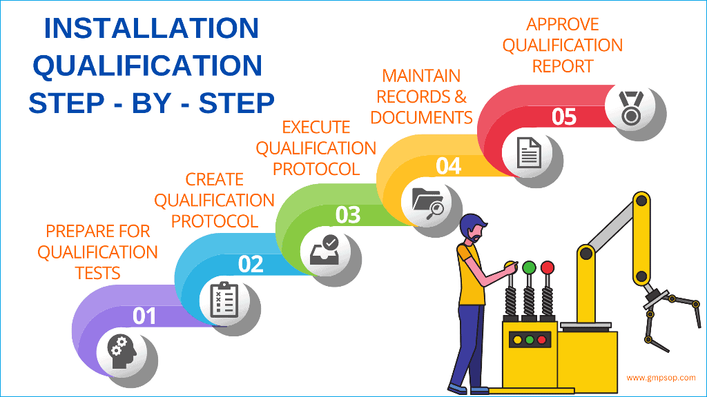
IQ is performed first because it:
Establishes baseline manufacturing conditions
Confirms equipment configuration and utilities
Locks approved software and hardware versions
Creates traceable records for future audits
Without IQ, subsequent validation activities such as OQ and PQ lack regulatory credibility.
Which Equipment and Systems Are Included in Medical PCBA IQ?
At Best Technology, IQ for medical PCBA projects typically covers:
SMT pick-and-place machines, including placement accuracy and software revision
Solder paste printing systems and stencil alignment capability
Reflow and curing ovens, including zone configuration and atmosphere control
AOI, SPI, and X-ray inspection systems
Electrical and functional test platforms
ESD protection infrastructure
MES-based traceability systems
Calibration tools and measurement equipment
Each item is verified against predefined installation requirements, including environmental conditions, utilities, configuration, and calibration status.
Why Is IQ Required for Medical PCBA Compliance?
Medical regulations such as ISO 13485 emphasize process control over final inspection. IQ provides documented proof that the manufacturing environment is controlled, repeatable, and auditable.
IQ is essential because it:
Prevents undocumented equipment substitution
Establishes a validated baseline for audits
Supports long-term traceability for regulated devices
Reduces regulatory risk during design transfer and scale-up
Without IQ, even functional medical PCBAs may be considered non-compliant during audits.
What Are the Risks of Skipping or Weak IQ in Medical PCBA?
Incomplete or missing IQ documentation can lead to:
Audit nonconformities
Delayed supplier qualification
Re-validation requirements
Increased regulatory exposure for OEMs
Even when PCBAs pass electrical testing, lack of IQ can result in formal non-acceptance during audits or regulatory reviews.
How Does Best Technology Implement IQ for Medical PCBA Projects?
Best Technology applies a structured IQ approach that includes:
Approved equipment lists and installation records
Verification of utilities and environmental conditions
Calibration status confirmation
MES and traceability validation
Controlled documentation aligned with medical audits
This ensures a repeatable and defensible foundation for all downstream validation activities.
What is the Relation Between IQ and OQ?
IQ confirms that the manufacturing environment is correctly installed, but it does not validate process performance. Once installation is confirmed, manufacturers must demonstrate that assembly processes operate reliably within defined limits. This is achieved through Operational Qualification (OQ).
In medical PCBA (Printed Circuit Board Assembly), IQ, OQ, and PQ are not procedural formalities; they are foundational controls that directly support patient safety, regulatory compliance, and long-term product reliability. Together, they form a structured validation framework required by global medical regulations and expected by auditors, OEMs, and notified bodies.
Regulatory Compliance Is Not Optional in Medical PCBA
Medical electronic assemblies fall under strict regulatory frameworks such as ISO 13485, FDA 21 CFR Part 820, and EU MDR. These regulations explicitly require manufacturers to validate production processes, not merely inspect finished products.
IQ, OQ, and PQ collectively demonstrate that:
The manufacturing environment is suitable
The process is capable and controlled
The output is consistently compliant
Without documented IQ/OQ/PQ evidence, a medical PCBA supplier will fail audits, risk regulatory findings, or cause customer design transfer delays.
IQ (Installation Qualification): Proving the Factory Is Correctly Set Up
IQ answers one fundamental question:
Is the equipment and infrastructure installed exactly as required?
Can we repeatedly build compliant medical PCBAs under real production conditions?
PQ involves:
Running multiple production lots
Using trained operators
Normal shift conditions (not engineering trials)
Measuring yields, defects, and key quality metrics
Typical PQ evidence includes:
First-pass yield (FPY)
Defect per million (DPMO)
Functional test pass rates
Reliability screening results (as applicable)
Why PQ is critical for medical PCBA programs:
Confirms stability over time, not just once
Supports design transfer from prototype to volume
Reduces field failure risk
Protects OEMs from recalls and liability exposure
For implantable, life-support, or diagnostic devices, PQ is often scrutinized line-by-line during audits.
Risk Reduction and Patient Safety
Medical PCBAs frequently operate in:
Life-critical systems
Continuous-use environments
High-reliability diagnostic platforms
IQ/OQ/PQ validation directly reduces:
Latent solder joint defects
Intermittent electrical failures
Process drift over long production cycles
Human variability in assembly steps
In medical applications, a single uncontrolled process variable can translate into patient harm. Validation converts unknown risks into controlled, documented ones.
OEM Confidence and Long-Term Supply Stability
From a customer perspective, IQ/OQ/PQ:
Shortens supplier qualification timelines
Simplifies regulatory submissions
Enables faster scale-up
Reduces ongoing audit burden
Medical OEMs increasingly select PCBA partners based on validation maturity, not just price or capacity.
A supplier that can present complete IQ/OQ/PQ documentation is signaling long-term manufacturing discipline and regulatory readiness.
Why IQ, OQ, PQ Are Non-Negotiable for Medical PCBA?
In medical PCBA manufacturing:
IQ proves the factory is correctly installed
OQ proves the process is technically capable
PQ proves consistent, real-world performance
Together, they ensure:
Regulatory compliance
Process stability
Product reliability
Patient safety
Medical electronics demand more than “working boards.” They demand validated processes that work every time.
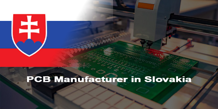
The PCB manufacturer in Slovakiaplays a crucial role in Europe’s electronic supply chain, offering diverse solutions for industrial, automotive and medical sectors. With mature industrial foundations and proximity to European markets, PCB manufacturer in Slovakiacontinues to expand their service scope, while facing fierce global competition. This blog covers top players, pain points, selection guides and future trends of Slovakia PCB, providing practical value for relevant businesses seeking reliable Slovakia PCB manufacturer.
Top 10 PCB Manufacturer in Slovakia
Company Name
Main Business
Core Advantages
Process Capabilities
Lead Time
EBest Circuit Co., Limited( Best Technology)
Multilayer/HDI/rigid-flex PCB
Global supply chain, EU compliance
1-32 layers, 3mil/3mil, blind vias
2-7 days
SQP International s.r.o
Multilayer/RF/turnkey PCB
30+ years, ISO 9001/14001, defense/medical
≤12 layers, <100µm lines, filled vias
2-5 days
UET PCB s.r.o
PCB fabrication/PCBA
99.99% yield, IATF16949/ISO13485
1-16 layers, Rogers/Isola, impedance
3-8 days
SVI Slovakia s.r.o
PCBA/box build/EMS
11,400㎡ facility, EU near-shoring
SMT/THT, 01005, vapor phase
4-10 days
GPV Electronics SK (H) s.r.o
PCBA/ODM/box build
Bratislava/Vienna logistics, lean
SMT/THT, burn-in, volume production
5-12 days
GPV Electronics SK (N) s.r.o
Prototyping/NPI/testing
17,000㎡ plant, 720 staff (since 1967)
High-volume SMT, system assembly
3-9 days
CRT Electronic s.r.o
Industrial PCBA
13+ years EU expertise, tailored
SMT/THT, small-batch, testing
3-8 days
Elcom s.r.o
Contract EMS/PCBA
R&D capability, cash register focus
Custom assembly, functional testing
4-10 days
Elpro s.r.o
SMT/THT assembly
In-house equipment, small-volume
Vacuum manipulators, reflow oven
3-7 days
SMT-Innovation s.r.o
SMT/assembly/equipment
20+ years EU experience, global
High-precision SMT, process optimization
2-8 days
Pain Points of PCB Manufacturer in Slovakia
Local Slovakia PCB factory lack ultra-fine line prototype capacity (below 3mil/3mil), relying on cross-border imports that extend lead times by 3-5 working days.
RoHS compliance pre-inspection for custom RF and high-Tg materials lengthens testing cycles, and small-batch prototype costs are 20-30% higher due to limited local scale.
Strict EU environmental regulations and high labor costs raise expenses for Slovakia PCB manufacturer, while mixed-brand equipment cuts efficiency by 10-15%.
Insufficient localized DFM support and specialized tools prolong design iterations for Slovakia PCB design, constrained by miniaturization and production limits.
Severe skilled labor shortage forces Slovakia PCB assembly plants to automate, yet 01005 component assembly still depends on limited skilled staff.
RoHS-compliant component supply disruptions and post-assembly testing add 1-2 working days to lead times, delaying production continuity.
How to Choose A Reliable PCB Manufacturer in Slovakia?
Verify Certification Qualifications: Prioritize manufacturers holding ISO 9001 (general quality), IATF 16949 (automotive-grade), and ISO 13485 (medical-grade) certifications—over 90% of leading Slovakia PCB factory possess these. Additionally, confirm UL certification and UL 94V0 flame retardant rating to ensure compliance.
Evaluate Process Capabilities: Beyond verifying 3mil/3mil line width accuracy and 12+ layer production capacity, check support for high-end materials like Rogers/Isola, blind/buried via technology, and ±1µm impedance control to meet precision requirements.
Control Yield Rate and Inspection: Optimize for manufacturers with a yield rate of ≥99.5%. For instance, UET PCB achieves a 99.99% yield rate through full-process quality inspection including AOI (Automatic Optical Inspection) and flying probe testing, ensuring mass production stability.
Consider Lead Time and Supply Chain: Confirm capacity for urgent prototypes (2-3 days) and mass production (5-7 days). Meanwhile, check inventory of core materials such as FR-4 and high-Tg substrates, as well as the dedicated processing mechanism for urgent orders.
Prefer One-Stop Services: Prioritize end-to-end services provided by a Slovakia PCB company, including DFM optimization, component sourcing, PCBA assembly, and after-sales functional testing to reduce collaboration costs.
Validate Supply Chain Stability: Understand partnerships with leading material suppliers (e.g., Isola, Rogers) to ensure supply of RoHS 3 compliant materials and avoid supply disruption risks.
Confirm Cost Transparency: Request a detailed quotation breakdown to clarify additional fees for testing, expediting, and customization, avoiding hidden costs that align with local production budget needs in Slovakia.
How to Evaluate the Lead Time of Slovakia PCB Manufacturer?
Order priority system: Confirm the manufacturer’s expedited service levels (e.g., 24/48-hour turnaround) for urgent orders and corresponding cost breakdowns to avoid hidden fees.
Raw material inventory: A reliable Slovakia PCB plant maintains ≥80% stock of core materials (FR-4, Rogers) to shorten material procurement cycles for standard orders.
Production schedule transparency: Require real-time order tracking tools to monitor progress and proactively alert for potential delays.
Equipment maintenance plans: Check scheduled maintenance protocols and target unplanned downtime rate (≤2% monthly) to minimize production disruptions.
Logistics partnerships: Prioritize manufacturers near Bratislava’s EU logistics hub, enabling next-day delivery to key European markets.
Batch size adaptability: Verify that lead time scales rationally, small batches should not incur excessive delays vs. mass production.
Quality control efficiency: Ensure in-line QA processes (AOI testing) to reduce rework, as post-production fixes can extend lead times by 1-2 days.
How to Evaluate the Production Capacity of Slovakia PCB Manufacturing Company?
Facility scale: Assess production area by tiers, small (≥2,000㎡) for batches, medium (≥8,000㎡) for stable mass output, and large (≥15,000㎡, e.g., GPV Electronics’ 17,000㎡ plant) for high volume. Top Slovakia PCB factory achieve ≥60% automation for core processes.
Machine precision: Confirm equipment supports fine-line fabrication (high-end 50µm, mainstream <100µm like SQP International), ±1µm LDI accuracy, and blind/buried via compatibility for Slovakia PCB.
Monthly output: A capable PCB manufacturer in Slovakia hits 30,000-50,000㎡/month (medium scale) and 50,000+㎡/month (large scale) to match local demand.
Quality control system: Require 100% AOI/X-ray testing for high-precision orders, target defect rate ≤0.3% (industry avg: 0.5-0.8%), and prioritize manufacturers like UET PCB with 99.99% yield rate.
Material sourcing network: Validate Isola/Rogers partnerships with 48-hour emergency replenishment, and ensure 100% RoHS 3 compliant suppliers.
Staff expertise: For medium facilities, require ≥50 skilled workers (80%+ IPC-A-610 certified) and ≥40 annual training hours per staff.
Certification scope: Confirm IPC Class 2/3 compliance (85% of top Slovakia PCB company meet this), plus IATF 16949 (automotive) and ISO 13485 (medical).
Future Challenges for Slovakia PCB Manufacturer
Rising labor costs in Slovakia, narrowing price gaps with Asian manufacturers.
Increased R&D investment pressure for advanced technologies (HDI, flexible PCB).
Stricter EU environmental regulations (RoHS 3 updates) raising production costs.
Shortage of high-tech talent for complex PCB manufacturing and design.
Supply chain volatility due to global component shortages and geopolitical risks.
Competition from neighboring EU countries (Austria, Germany) with mature PCB industries.
Demand for miniaturization pushing equipment upgrade costs for ultra-fine line production.
Shift to green manufacturing requiring eco-friendly materials and processes.
FAQs of Slovakia PCB Manufacturing
Q1: How to resolve microcracks in PCB substrates during production? A1: Microcracks stem from thermal stress and inferior materials. A professional PCB manufacturer in Slovakia uses high-grade substrates (Isola, Rogers) with stable thermal expansion and controls soldering temperature swings within ±5°C, plus thermal cycling (-40°C to 85°C) in prototype testing to eliminate defects.
Q2: Why do PCB prototypes have inconsistent impedance values, and how to fix it? A2: Inconsistency comes from imprecise line width and material variations. Slovakia PCB manufacturing adopts laser direct imaging (LDI) for ±1µm accuracy, pre-tests substrate batches, and provides DFM feedback to achieve 99.8% accuracy for impedance-controlled prototypes.
Q3: How to reduce delamination issues in multilayer PCB production? A3: Delamination is caused by moisture absorption and improper lamination pressure. An ISO 14001-certified Slovakia PCB plant conducts pre-baking (120°C for 4 hours), uses 35-40 psi vacuum lamination, and maintains humidity levels <45%.
Q4: What causes solder bridging in PCBA, and how to prevent it? A4: Solder bridging results from faulty stencil design and component placement. Automated SMT lines (10,500 components/hour) with optical centering, laser-cut stencils (0.1mm precision), and post-soldering AOI testing prevent this issue.
Q5: How to shorten lead time for custom high-Tg PCB orders in Slovakia? A5: Long lead times arise from material shortages and poor scheduling. A reliable PCB manufacturer in Slovakia stocks high-Tg materials (Tg 170°C+) and uses in-house production to offer 2-3 day prototype lead times for custom orders.
Looking forPCB Malta manufacturer? This blog covers main pain points of Malta PCB manufacturer and our solutions to these points.
Malta’s electronics industry relies heavily on reliablePCB Malta manufacturerand high-quality PCB manufacturing Malta services. As demand for precision electronics grows locally, sourcing a trustworthy PCB manufacturer in Malta becomes crucial for seamless production workflows. This guide covers the top local players, core industry pain points, and how leading local manufacturers deliver tailored solutions aligned with Malta’s unique production needs and EU compliance standards.
Top PCB Malta Manufacturer in 2026
Company Name
Main Business
Core Advantages
Process Capability
Lead Time
EBest Circuit Co., Limited
PCB prototyping/mass production/HDI boards
19-year experience, 24h urgent prototyping
40-layer HDI, 0.1mm line width
24hrs-15 days
Electronics Malta Group
Consumer electronics PCBs
Cost-effective, RoHS compliance
16-layer, flexible substrate
4-18 days
Malta Electronics Solutions OÜ
Medical PCB
ISO13485, cleanroom
24-layer, biocompatible
12-22 days
TechPrint Malta Ltd
Single/double-layer PCBs
Fast small-batch
Standard finishes
2-10 days
HDI Malta Electronics OÜ
HDI/telecom PCBs
REACH compliance
30-layer HDI, PTFE
14-25 days
GreenCircuit Malta Ltd
Eco-friendly PCBs
Waste recycling
Halogen-free
9-18 days
Pain Points of PCB Malta Manufacturer
Urgent PCB prototyping demands cannot be met, with standard lead times exceeding 7 days, delaying project progress.
Design flaws are detected late in production, leading to rework, increased costs, and extended timelines.
Inconsistent product quality across batches, with issues like board warpage and poor solderability affecting usability.
High material costs for special substrates (e.g., high-frequency, medical-grade) without cost-saving alternatives.
Limited process capability for complex designs, such as HDI boards with blind/buried holes and fine line widths.
Lack of professional support for PCB printing Malta, resulting in unclear silk-screen and poor mark visibility.
Unreliable delivery schedules, with frequent delays due to inefficient production planning.
Insufficient testing processes, leading to hidden electrical faults in finished PCBs.
Our PCB Solutions to These Pain Points
Pre-Production Design Support: Provide free DFM analysis to identify potential design flaws early, avoiding rework. Our team optimizes designs for manufacturability while maintaining performance, addressing late-stage design issue pain points.
Flexible Prototyping Service: Offer 24-hour urgent PCB prototyping and 3-7 day standard prototyping, fully meeting tight project schedules. Advanced automated lines ensure fast sampling without compromising quality.
Cost-Optimization Solutions: Cooperate with top substrate suppliers to provide cost-effective alternatives for special materials. Customize cost-sensitive plans based on production volume, reducing material cost burdens.
Advanced Process Capability: Master HDI, blind/buried hole, and fine line processing technologies to handle complex designs. Professional PCB printing Malta equipment ensures clear silk-screen and durable marks.
Strict Quality Control: Implement full inspection for mass production, including automated optical inspection (AOI), electrical testing, and board warpage detection. Achieve consistent quality across batches with a 99.8% pass rate.
MES System Full-Process Traceability: MES enables real-time production monitoring and full-process traceability, covering raw material intake, processing, testing, and delivery. Clients access real-time progress to avoid delivery doubts. MES-driven smart planning ensures 99.2% on-time delivery.
Post-Delivery Support: Offer technical consultation and fault analysis for finished products. Provide rework solutions for any quality issues, ensuring worry-free use of PCB Malta products.
Why Choose EBest(Best Technology) asPCB Malta manufacturer?
24-Hour Urgent Prototyping: Unique rapid production lines complete PCB prototyping within 24 hours, the fastest in the Malta market for urgent orders.
Competitive Pricing: 19 years of industry experience enables optimized supply chains, offering 10-15% lower costs than peers for the same quality PCB manufacturing Malta.
Cost-Sensitive Solutions: Customize material selection and process plans based on project needs, reducing unnecessary expenses without sacrificing performance.
High On-Time Delivery Rate: 99.2% of orders are delivered on schedule, supported by smart production scheduling and sufficient inventory.
Strict Quality Control: Mass production adopts 100% full inspection, with 8-stage quality checks from material incoming to finished product delivery, ensuring stable quality.
Rich Industry Experience: 19 years of serving global clients helps optimize designs and processes, reducing overall project costs by 8-12%.
Free DFM Analysis: Professional team provides detailed design optimization suggestions before production, eliminating rework risks.
Comprehensive Certifications: Hold ISO9001:2015, ISO13485:2016, REACH, RoHS, and IATF16949 certifications, meeting diverse industry requirements.
One-Stop Service: Integrate PCB printing Malta, prototyping, mass production, and testing, simplifying procurement processes for clients.
Localized Support: Set up a local service team in Malta to provide fast technical consultation and after-sales support, responding within 2 hours.
Our PCB Rapid Prototyping Service
EBest’s PCB rapid prototyping service prioritizes speed to meet our clients’ urgent project needs. With four dedicated express production lines, we achieve a 99.5% on-time delivery rate for 24-hour expedited prototyping, 50% faster than the average in the Maltese market. Even for complex PCB designs, from single-layer boards to 40-layer HDI prototypes, we maintain the same rapid turnaround time, thanks to the strong support of high-precision exposure machines and automated processing equipment. Each prototype undergoes 18 rigorous quality checks (including AOI optical inspection and impedance testing), ensuring a 99.8% yield rate, consistent with mass production standards. Whether you face last-minute design adjustments or urgent project deadlines, our expedited service delivers reliable Maltese PCB prototypes on time, helping you shorten development cycles and gain a competitive edge in the market.
Background: A Malta industrial automation equipment firm required high-reliability PCB Malta for its new control system, targeting harsh industrial environments with strict temperature stability and anti-interference for 2GHz high-frequency signals.
Requirements: 16-layer HDI PCB, operating temperature -40℃ to 85℃ (1,000-hour thermal cycle resistance), impedance control ±5% for 2GHz signals, prototype lead time ≤10 days, mass production (5,000 units) ≤20 days.
Difficulties: Impedance stability control for 2GHz high-frequency signals (industry standard Df ≤0.01), 16-layer lamination risk of board warpage exceeding IPS standard (≤0.75%), and compressed lead time 30% shorter than market average.
Solutions: Adopted high-temperature FR-4 substrate (Tg 180℃) and optimized lamination parameters (180℃/350PSI) to control warpage ≤0.5%; Used precision etching (±0.02mm tolerance) with 3 rounds of impedance calibration tests; Allocated dedicated expedited lines via MES scheduling for time guarantee.
Results: Prototypes delivered in 7 days, 5,000 mass-produced units in 18 days (10% faster than required). All passed 1,000-hour thermal cycle and 2GHz anti-interference tests, with 100% pass rate and warpage ≤0.4%. The client launched on schedule, and 60% of their subsequent industrial control projects designate us as the exclusive PCB manufacturer in Malta.
FAQs of PCB Manufacturing Malta
Q1: How to avoid board warpage in multi-layer PCB production? A1: We optimize lamination parameters (temperature, pressure, holding time) and adopt symmetric layer design to balance stress. Post-production mechanical correction and thermal aging treatment further reduce warpage. Contact us for customized warpage control solutions for your PCB Malta project.
Q2: Can design flaws be detected before PCB prototyping? A2: Yes. We provide free DFM analysis to check for design issues like unreasonable line width/space, improper hole size, and silk-screen conflicts. This reduces rework rates by over 90%. Reach out for pre-production design validation.
Q3: What surface treatment is best for PCB printing Malta in humid environments? A3: Immersion gold or OSP surface treatment is recommended for humid conditions, as they offer excellent corrosion resistance. We can tailor surface treatment plans based on your application environment. Inquiry now for personalized suggestions.
Q4: How to reduce costs for small-batch PCB manufacture Malta? A4: We offer shared mold services and optimize material cutting to reduce waste. Our cost-sensitive solutions can lower small-batch production costs by 10-15%. Contact us to get a cost-saving quote.
Q5: What tests are conducted for medical PCB products? A5: Medical PCBs undergo electrical testing, insulation resistance testing, biocompatibility testing, and temperature cycle testing, complying with ISO13485 standards. We provide full test reports for each batch. Inquiry for medical-grade PCB prototyping and production services.
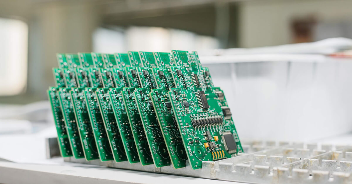
An SMT PCB board is a printed circuit board designed for surface mount technology, where electronic components are mounted directly onto copper pads on the board surface rather than inserted through drilled holes. This approach allows components to sit flat against the PCB, enabling compact layouts, shorter electrical paths, and efficient automated assembly through reflow soldering. As a result, SMT PCB boards support higher component density while maintaining consistent solder quality.
What Is an SMT PCB?
An SMT PCB is a printed circuit board designed specifically for surface mount technology, where electronic components are mounted directly onto copper pads on the surface of the board. Unlike traditional assembly methods, components do not use long wire leads inserted through drilled holes. Instead, they sit flat against the PCB and are soldered in place using controlled reflow processes.
This structural change enables much higher component density. Components can be placed on both sides of the board, and spacing between parts can be significantly reduced. As a result, SMT PCB boards are smaller, lighter, and more electrically efficient than older designs.
Another key benefit is manufacturing consistency. SMT placement is highly automated, allowing machines to position thousands of components per hour with exceptional accuracy. This repeatability improves yield and reduces defect rates, especially in high-volume production.
SMT PCB boards are now standard across consumer electronics, medical equipment, industrial controls, automotive electronics, and communication systems.
How Does SMT Impact PCB Design?
SMT influences PCB design from the earliest layout stage. Because surface-mounted components have short electrical paths, signal integrity improves, especially in high-speed and high-frequency circuits. This allows designers greater flexibility when routing traces and managing impedance.
Pad design becomes a critical factor in SMT layouts. Pad size, shape, and spacing directly affect solder joint quality and long-term reliability. Improper pad geometry can lead to solder bridging, tombstoning, or weak joints, all of which increase rework risk.
Layer stack-up also changes with SMT. Multilayer boards are common, as designers use internal planes for power distribution and noise control. Thermal management becomes more important as well, since compact components can generate localized heat that must be dissipated efficiently.
Finally, SMT PCB design must align with assembly equipment capability. Package size limits, placement tolerances, and inspection access all influence layout decisions.
Is SMT the Same as SMD?
SMT and SMD are closely related terms, but they are not interchangeable. SMT stands for surface mount technology and refers to the manufacturing process used to assemble components onto a PCB. SMD stands for surface mount device and refers to the component itself.
In simple terms, SMT is the method, while SMD is the part. Factories use SMT processes to place SMD components onto SMT PCB boards.
What Is the Difference Between SMD and SMT PCB?
An SMT PCB describes both the board design and the assembly method, while an SMD describes only the component package. SMT PCBs are designed with specific land patterns that support surface-mounted components and reflow soldering processes.
SMD components include chip resistors, capacitors, integrated circuits, and discrete semiconductors packaged for surface mounting. Without an SMT-compatible PCB, SMD components cannot be properly assembled or soldered.
In practice, SMT PCBs and SMD components always work together, but their roles are distinct.
How Does PCB Board SMT Differ From Through-Hole Assembly?
The difference between SMT and through-hole assembly is structural and operational. Through-hole assembly uses drilled holes where component leads pass through the board and are soldered on the opposite side. SMT places components directly onto surface pads without penetrating the board.
SMT enables much higher component density and allows assembly on both sides of the PCB. This supports smaller board sizes and more complex functionality. Through-hole assembly, while mechanically robust, occupies more space and limits layout flexibility.
SMT also supports full automation, while through-hole assembly often requires manual or semi-automated steps. This difference has a significant impact on cost and scalability. However, some products use both methods together, such as board assembly SMT DIP PCB or board assembly SMT THT PCB designs, where connectors or power components still benefit from through-hole strength.
What Is the Major Advantage of Using SMT?
The primary advantage of SMT PCB assembly is efficiency at scale. Automated placement machines operate at high speed with consistent accuracy, enabling reliable mass production. This efficiency directly reduces assembly time and labor costs.
SMT also supports miniaturization. More functionality fits into less space, enabling thinner, lighter, and more portable devices. Electrical performance improves as well, since shorter lead lengths reduce parasitic effects and signal noise.
Reliability benefits from controlled soldering processes. Reflow soldering produces uniform joints, reducing variation and long-term failure risk.
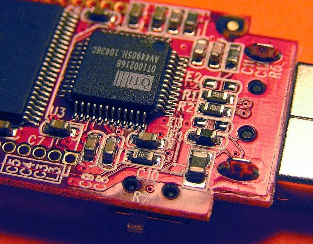
What Components Are Used in SMT?
SMT supports a wide range of electronic components. Common passive parts include chip resistors and capacitors in standardized package sizes. Integrated circuits appear in formats such as SOIC, QFP, QFN, and BGA, supporting everything from simple logic to advanced processors.
Discrete components like diodes, transistors, and MOSFETs are widely used in SMT designs. Many connectors and RF modules are also available in surface-mount packages, allowing compact system integration.
Each component type requires proper footprint design, accurate stencil thickness, and precise placement to ensure reliable solder joints. Successful SMT PCB assembly depends on matching component selection with process capability.
What Quality Checks Are Used in SMT PCB Assembly?
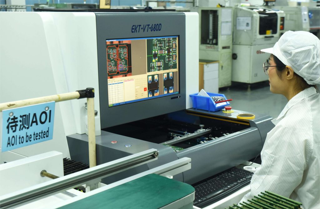
Quality control is central to SMT PCB assembly. Inspection begins with solder paste application, where volume and alignment are monitored to prevent downstream defects. Automated optical inspection then verifies component placement and visible solder joints.
For components with hidden connections, such as BGAs, X-ray inspection is used to evaluate internal solder quality. Reflow temperature profiles are carefully controlled to avoid thermal damage or weak joints.
Electrical testing confirms circuit continuity and functionality, while final inspection ensures cleanliness and cosmetic quality. These layered quality checks protect product reliability and customer confidence.
Where Do We Use SMT?
SMT is used across nearly every electronics sector. Consumer electronics rely on it for compact form factors and high functionality. Industrial and medical devices depend on SMT for precision, consistency, and long-term reliability.
Automotive electronics use SMT for control units and sensor systems that must withstand harsh conditions. Telecommunications and networking equipment rely on SMT to support high-speed signal performance and dense layouts.
As electronics continue to evolve, SMT PCB assembly remains a foundational technology enabling innovation at scale.
Conclusion:
An SMT PCB board is a circuit board built for surface mount technology, where components are placed on surface pads and soldered by reflow for fast, repeatable production. Compared with through-hole assembly, SMT PCB assembly supports higher density, smaller products, and strong electrical performance, which is why it dominates modern electronics.
To learn more about how Best Technology supports these SMT PCB assembly technologies, please contact us at sales@bestpcbs.com
Latvia’s PCB manufacturing sector boasts reliable production capabilities and strict quality control, making PCB Latvia manufacturer a trusted choice for regional electronic projects. With a manufacturing capacity utilization rate of 75.1% in late 2025, the industry balances precision and efficiency to meet diverse project needs. Whether for prototyping or mass production, PCB Latvia manufacturer integrates advanced technologies and European standards, solidifying its position in the Baltic electronic supply chain. This guide covers top suppliers, quality benchmarks, pain points, and selection strategies to support informed decisions for Latvia PCB projects.
Top 10 PCB Manufacturer in Latvia
Company Name
Main Business
Core Advantages
Process Capability
Lead Time
EBest Circuit Co., Limited
Metal core PCB design/fabrication
18-year experience, ISO certified, 30,000㎡ factory
Quality Certifications for PCB Latvia Manufacturer
ISO 9001:2015: A baseline mandatory certification for Latvia PCB company operations. It establishes a standardized quality management system, covering production processes, raw material inspection, and after-sales service to ensure consistent product quality.
RoHS Certification: An EU mandatory environmental certification for electronic products. It restricts the use of 10 hazardous substances (e.g., lead, mercury) in Latvia PCB manufacturing, with lead content limited to ≤0.1% to comply with EU environmental directives.
REACH Certification: Another EU mandatory environmental certification. It regulates the registration, evaluation, authorization, and restriction of chemicals used in Latvia PCB plant production, ensuring no harmful substances pose risks to human health and the environment.
CE Certification: A mandatory safety certification for products entering the EU market. All PCB Latvia products must obtain CE marking, proving compliance with EU technical directives including EMC and safety requirements.
ISO 13485: Mandatory for Latvia PCB manufacturer serving the medical industry. It specifies quality management system requirements for medical device-related PCBs, ensuring compliance with medical industry safety and effectiveness standards.
IATF 16949: Essential for Latvia PCB factory supplying the automotive sector. This certification aligns with global automotive industry quality standards, covering production control, traceability, and defect prevention for automotive-grade PCBs.
IPC-A-610: A mandatory assembly quality standard. It defines acceptability criteria for Latvia PCB assembly processes, ensuring soldering, component mounting, and wiring meet industry-wide quality benchmarks.
Pain Points of PCB Latvia Manufacturer
High material costs due to reliance on imported high-grade substrates, increasing per-unit production expenses for small-batch orders.
Limited local supply chain for specialty components, leading to delays when sourcing custom materials or obsolete parts.
Capacity constraints with average utilization at 75.1%, making it challenging to handle sudden surge in large-volume orders.
Strict EU environmental regulations raising production costs for waste treatment and sustainable material adoption.
Technical gaps in high-layer HDI PCB fabrication, limiting ability to cater to advanced electronic project requirements.
Inconsistent lead times caused by cross-border logistics delays for raw materials and component shipments.
1. Certification & Compliance Standards: Prioritize ISO 9001, UL, or IEC 61190-certified suppliers (e.g., ALMIKO Ltd, VOLBURG Ltd) to ensure quality control and regulatory adherence. Verify certifications via official directories.
2. Technical Capabilities & Specialization: Assess capabilities for multi-layer PCBs (up to 24+ layers), HDI (High Density Interconnect), impedance control, and materials (e.g., FR4, Rogers). ALMIKO Ltd, for example, supports Gerber/Excellon file formats and offers stencil production. Avoid suppliers lacking advanced tech documentation (e.g., layer stack-up details).
3. Turnaround Time & Logistics: Evaluate lead times, ALMIKO provides 3–15 working days (negotiable), with logistics via DHL/FedEx. European-based suppliers (e.g., Riga-based) reduce dependency on cross-border delays. Confirm DDP/DDU terms for cost transparency.
4. Cost Structure & Transparency: Analyze pricing models, setup fees, per-unit costs, and hidden charges (e.g., tooling, testing). IBISWorld reports the 2026 Latvian PCB market size at €78.6M, with 30 companies, compare quotes across 3+ suppliers to identify competitive rates.
5. Customer Support & Communication: Prioritize suppliers with 24/7 technical support (e.g., ALMIKO’s 25-year experience) and multiple communication channels (email/phone). Verify responsiveness through client reviews or direct inquiries. Avoid firms with opaque communication.
6. Supply Chain Resilience: Check component sourcing capabilities (e.g., ALFA RPAR AS’s local component supply network) to mitigate raw material shortages. European suppliers often align with REACH/RoHS standards, ensuring compliance.
7. Case Studies & References: Request case studies for similar projects (e.g., aerospace/industrial PCBs) to gauge reliability. ALMIKO’s portfolio includes prototypes and volume production, validate claims via client testimonials.
8. Scalability & Flexibility Confirm ability to scale from prototypes to mass production. Suppliers like VOLBURG Ltd offer box-build services, accommodating growing project needs. Avoid fixed-capacity manufacturers for dynamic projects.
How to Inspect the Quality Management System of PCB Latvia Manufacturer?
Verify the validity and pertinence of certifications: Confirm ISO 9001:2015 certification is issued by EU-recognized bodies (e.g., TÜV, SGS). For medical orders, ensure ISO 13485 covers cleanroom control; for automotive, IATF 16949 must include PPAP documentation support, which is a core requirement for Latvia PCB manufacturer serving high-end industries.
Review process-specific quality control plans: For drilling, plating and solder mask application, check if plans include parameter tolerances (e.g., drilling hole diameter ±0.02mm), inspection frequency (once per 50pcs) and SOP (Standard Operating Procedure) alignment with IPC standards, ensuring each key process has measurable control points.
Validate full-chain traceability systems: Ensure each batch is trackable via digital codes (Ecode or commodity barcode) from raw material batch numbers, production equipment IDs to finished product testing data. The system should enable locating problematic batches within 2 hours to minimize losses.
Assess in-house testing coverage and precision: Confirm X-ray inspection achieves ≥99.2% defect detection rate, solderability tests comply with IPC-J-STD-002, and impedance measurement maintains ±5% tolerance for high-frequency Latvia PCB. Prioritize factories with SPC (Statistical Process Control) data for test results.
Request customer complaint and correction records: Focus on 12-month data: top PCB manufacturer in Latvia maintains a complaint rate ≤0.3%. Check if each complaint has root-cause analysis, rectification measures (completed within 72 hours) and follow-up verification to prevent recurrence.
Confirm LVS and CE compliance: LVS must cover electrical safety, EMC (Electromagnetic Compatibility) and environmental indicators; CE marking should be supported by full test reports. Verify quarterly audit records from Latvia’s Consumer Rights Protection Center to ensure ongoing compliance.
Evaluate employee training and qualification: Check if new staff receive 100-hour pre-job training on IPC-A-600/IPC-610, and in-service staff have semi-annual refresher courses. Require qualification certificates for key positions (e.g., plating, testing) with a passing rate ≥95%.
How to Evaluate the Production Capacity of Latvia PCB Manufacturer?
Evaluation Guide to Quality Management System of PCB Latvia Manufacturer:
Confirm monthly production capacity to match your order scale: Use ICAPE-MMAB’s 550 sqm/month as a reference and verify alignment with your batch size. Ensure it stably handles small batches (≤500pcs) or large-volume orders (≥1000pcs) without efficiency loss.
Verify process coverage: Check maximum layer count (local factories mostly cover 1-14 layers; ultra-high layers over 16 require external cooperation), substrate range (FR-4, aluminum, high-frequency materials) and special processes (heavy copper up to 10oz, V-groove, HDI microvias).
Evaluate core equipment performance: Focus on CNC drilling machines (±0.02mm accuracy), AOI systems (≥99% defect detection rate) and supporting equipment such as electroplating lines and exposure machines to ensure process stability.
Assess small-batch and prototype flexibility: Most Latvia PCB plants excel in quick-turn prototypes. Confirm prototype turnaround (3-5 days for ≤10pcs) and changeover efficiency (≤2 hours between different designs) to fit agile production needs.
Audit raw material supply reliability: Secure stable access to FR-4, high-frequency (Rogers/PTFE) and metal substrates. Confirm backup suppliers to avoid 2-3 week delays for imported materials common in the region.
Check peak demand response capacity: Confirm shift arrangements (2-3 shifts daily) and overtime capability. Top PCB manufacturer in Latvia can boost production capacity by 30% through overtime to meet tight deadlines.
How to Evaluate the Delivery Time of PCB Manufacturing Company Latvia?
Clarify standard/expedited lead times by order volume: Prototypes (≤10pcs): 3-5 days standard, 24-48 hours expedited. Small-batch (100-500pcs): 7-10 days; mass production (≥1000pcs): 10-15 days. Confirm upfront expedited costs (5%-15% of order value) with a PCB Latvia manufacturer.
Confirm local delivery zones and logistics: Riga/Zone I: 1-day DPD delivery (2% failure rate). Zone III remote areas: 2-3 days via TNT. Check if the Latvia PCB factory covers secondary delivery costs for damaged goods.
Check delayed delivery penalties and compensation: Reliable partners include 0.5% daily order value deduction (capped at 10%) for delays in contracts. Confirm compensation for critical orders (free expedited rework, priority fulfillment).
Evaluate standard material inventory: Prioritize factories with ≥90% common substrate (FR-4, aluminum) coverage in local warehouses. Check inventory turnover (7-14 days ideal) and safety stock (supports 30% monthly volume) for faster Latvia PCB fulfillment.
Assess supply chain contingency plans: Confirm alternative material suppliers (48-hour response) to mitigate 2-3 week delays of imported high-frequency materials. Verify backup production capacity for downtime.
Request 6-month OTIF data: Target 95%+ OTIF (exceeds 82% regional average). Ask for order-type breakdown and third-party verification from the PCB manufacturer in Latvia.
Clarify custom process impact on lead times: HDI microvias (+2 days), rigid-flex (+3-4 days), heavy copper (≥6oz, +1-2 days). Discuss optimization to reduce extensions for Latvia PCB manufacturing.
FAQ of Latvia PCB Manufacturing
Q1: How to resolve PCB panel warping during production? A1: We use balanced copper layer design and controlled thermal processes to minimize warping. Our pre-preg material selection (matched to substrate Tg) reduces warpage rate to below 0.5%. Contact us for a custom DFM review to optimize panel design.
Q2: Why do prototypes have longer lead times in Latvia, and how to speed this up? A2: We maintain stock of standard FR-4 and aluminum substrates, enabling 3-day prototype turnaround. Our digital order system streamlines design approval, cutting 1-2 days from lead time. Inquire for our expedited prototype service. Q3: How to ensure impedance control for high-frequency Latvia PCB? A3: We use TDR impedance measurement equipment and tight process control (±5% tolerance). Our partnership with local material suppliers ensures consistent dielectric constant. Let us quote your high-frequency PCB project for tailored solutions. Q4: What causes solder mask adhesion issues, and how to prevent them? A4: Adhesion issues stem from inadequate surface cleaning. We implement plasma cleaning before solder mask application, achieving 99% adhesion rate. Our in-process testing catches issues early. Request a sample to verify quality. Q5: How to handle custom material requirements for Latvia PCB manufacturing? A5: We have a global supply chain for specialty materials (such as PTFE) with 7-day lead times, faster than local averages. Our material engineers help select alternatives if needed. Contact us to discuss your custom material specifications.
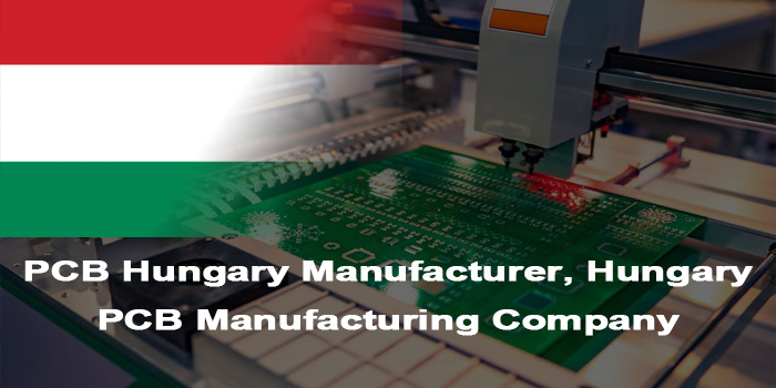
Hungary has emerged as a key hub for electronics manufacturing in Eastern Europe, attracting numerous PCB Hungary manufacturer and global firms setting up local production bases. As a professional PCB Hungary manufacturer, EBest Circuit Co., Limited (Best Technology Circuit Co., Limited) leverages local industrial advantages and global supply chain resources to deliver high-quality PCB Hungary solutions. The region’s PCB manufacturing sector benefits from labor cost advantages and proximity to European markets, while facing challenges like process consistency and supply chain stability that demand reliable Hungary PCB manufacturer partners.
Are You Facing These Challenges?
Are your PCB designs frequently rejected due to manufacturability issues, leading to repeated revisions and project delays?
Are you unable to find a Hungarian PCB factory that can provide 24-hour expedited prototyping services for small-batch, time-sensitive orders?
Do you encounter board warping and deformation issues after lamination or reflow soldering, affecting assembly yield?
Do you frequently experience communication difficulties with local Hungarian PCB companies, resulting in mismatched production requirements?
Are high raw material costs and exchange rate fluctuations making it difficult to control your Hungarian PCB manufacturing costs?
Is the quality inspection of your mass-produced PCBs insufficient, leading to a risk of defects after delivery?
Are you unable to obtain timely technical support in Hungary for specialized processes such as HDI or thick copper PCB manufacturing?
End-to-End Guarantee from Requirement to Delivery
Pre-Production Consultation: Provide free DFM analysis to identify design flaws in advance, avoiding revision delays and reducing Hungary PCB manufacturing costs. Our professional team delivers analysis reports with clear optimization suggestions for seamless cooperation.
Urgent Prototyping Support: 24-hour rapid prototyping service for time-sensitive orders, ensuring your project progresses as scheduled without waiting for standard lead times. We leverage global production resources to fulfill urgent demands for PCB Hungary projects.
Process Optimization: Adopt symmetric lamination and precise temperature control to eliminate board warpage, improving assembly yield for PCB Hungary products. Strict process parameters are standardized to ensure consistent quality across batches.
Dedicated Account Management: Assign exclusive account managers to handle your orders, providing scheduled progress updates and prompt responses to inquiries via email and phone. We ensure production requirements are accurately implemented through our global production network for Hungary-bound orders.
Cost Control: Offer cost-sensitive solutions based on 19 years of experience, optimizing material selection and process flow to offset raw material and exchange rate impacts. Customized plans help reduce overall Hungary PCB manufacturing costs effectively.
Full Inspection for Mass Production: Implement 100% AOI and X-Ray inspection in our PCB manufacturing process for Hungary orders, eliminating defective products before delivery. Inspection reports are provided to confirm quality compliance.
Special Process Capability: Master HDI, thick copper, and rigid-flex PCB technologies, with a professional technical team to solve bottlenecks. We support complex process requirements for Hungary PCB manufacturing projects.
On-Time Delivery Commitment: Rely on mature global supply chain management and automated production lines to achieve a 99.2% on-time delivery rate. Cross-border logistics optimization ensures timely arrival of PCB Hungary orders.
Why Hungarian Clients Choose EBest (Best Technology) for PCB Manufacturer?
19 Years of Industry Experience: Rich expertise in solving complex manufacturing challenges, helping customers reduce trial-and-error costs and shorten time-to-market.
Free DFM Analysis: Professional design review before production, identifying potential issues to avoid rework and improve Hungary PCB manufacturing efficiency.
24-Hour Urgent Prototyping: Dedicated production lines for emergency orders, completing PCB Hungary prototyping within 24 hours to meet tight project schedules.
Authoritative Certifications: Hold ISO9001:2015, ISO13485:2016, IATF16949, REACH, and RoHS certifications, meeting requirements for medical, automotive, and industrial electronics.
Competitive Pricing & Cost-Saving Solutions: Customized cost-sensitive plans based on project requirements, reducing overall Hungary PCB manufacturing costs by 15%-20% through process optimization.
High On-Time Delivery Rate: 99.2% order punctuality supported by MES production management system, ensuring stable supply for your production line.
Strict Quality Control: 100% full inspection for mass production, adhering to strict quality control processes that exceed industry standards for PCB Hungary products.
Verify Certification Compliance: Confirm IATF16949 (automotive) and ISO13485 (medical) certifications. Ensure EU RoHS (lead ≤0.1%) and REACH compliance, aligning with your product category to avoid penalties from misaligned credentials (impacting 12% of local orders yearly).
Test Urgent Prototyping Capability: Validate 24-hour quick-turn services via small trials. Confirm dedicated lines, ≥99.2% urgent prototyping yield, and transparent costs with urgent fees at 15%-30% of standard pricing. Avoid hidden fees with detailed quotes covering all process costs.
Review Quality Control Details: Request AOI (≥99.8% surface defect coverage) and X-Ray (≥99.5% BGA joints accuracy) data. Target batch defect rate ≤0.05% (half the 0.1% industry average), and clarify 48-hour quality response and replacement for batches over 0.03% defects.
Confirm Process Suitability: Ask for verifiable Hungary project cases for HDI, thick copper or high-frequency PCBs. Ensure impedance tolerance ±5%, micro-drill tolerance ±0.01mm, layer alignment error ≤5μm, and dielectric constant 3.5-4.5 for high-frequency PCBs.
Assess Delivery Stability: Check 12-month on-time rate ≥98% (exceeding the 95% local average). Inquire about supply chain contingencies, including local core material stock (minimum 2 weeks) and logistics partners with ≥99% on-time rates, plus ≤2% annual disruption rate.
Prioritize Value-Added Services: Optimize for free 1-hour DFM analysis, which cuts rework rates from 8%-12% to ≤3%. Ensure ≥95% 24-hour resolution for complex processes; DFM analysis also shortens lead time by 3-5 days on average.
Analyze Total Cycle Costs: Beyond unit prices, account for rework (7% of order value), late fees (1%-2% daily), packaging (2%-5%), and EU customs duties (0%-6%). Prefer 3-6 month price locks to mitigate volatility, as copper prices fluctuate ±18% yearly.
Clarify Communication Norms: Set 24-hour email response timelines and 99.9% accurate notifications for key order nodes. Define 8-hour confirmation for order adjustments, reducing delays from miscommunication (affecting 6% of orders).
How to Evaluate Production Capacity of PCB Hungary Manufacturer?
Inspect Equipment Precision & Efficiency: Verify automated SMT lines with ≥60,000 components/hour placement speed and ±0.03mm precision, AOI machines with ≥99.8% surface defect coverage, and micro-drilling equipment supporting minimum 0.1mm diameter with ±0.01mm tolerance.
Review Process Parameter Limits: Confirm maximum production layers (1-20 layers for high-capacity Hungary PCB factory), minimum line width 0.075mm, and minimum hole diameter 0.1mm, with impedance tolerance controlled within ±5% for high-frequency products.
Evaluate Daily Capacity & Batch Adaptability: Assess daily output (5,000-50,000 pieces for mass production, 100-500 pieces for small-batch) and order handling capability, ensuring ≤24-hour response for batches ≤500 pieces and stable yield ≥99.2% across batch sizes.
Check Supply Chain Stability: Confirm cooperation with top-tier material suppliers (e.g., Isola, Rogers for substrates; JX Nippon for copper foil), core material inventory ≥14 days, and supplier on-time delivery rate ≥99% to avoid production interruptions.
Assess Process Optimization Efficiency: Evaluate multi-variety order changeover time (≤2 hours for different PCB types) and process optimization effects, such as yield improvement ≥3% and production cycle reduction ≥15% via smart process adjustment.
Verify Quality Management Effectiveness: Check batch defective rate ≤0.05% (industry average 0.1%), customer complaint rate ≤0.3%, and ISO9001:2015-certified QMS with monthly quality review mechanisms.
Quantify Technical Problem-Solving Capacity: Confirm technical team size (≥15 professionals for mid-sized Hungary PCB manufacturer), complex process problem-solving rate ≥95%, and resolution time ≤24 hours for HDI/thick copper PCB issues.
Evaluate Scheduling & Urgent Order Flexibility: Ensure MES-based production scheduling system with real-time tracking, ≤2-hour response to urgent orders, and ability to handle ≤30% urgent orders without affecting standard order on-time rate (≥98%).
How to Evaluate Delivery Time of Hungary PCB Manufacturer?
Confirm standard delivery times: Clearly define delivery times for different order types and layer counts – prototyping (1-8 layers: 2-5 days; 10+ layers: 7-10 days) and mass production (1-8 layers: 3-8 days; 10+ layers: 10-15 days), consistent with the average standards of the Hungarian PCB manufacturing industry.
Assess urgent order handling capabilities: Verify 24/48-hour delivery capabilities, with urgent order fees at 15%-30% of the standard price. Ensure on-time delivery rate for urgent orders is ≥99%, and that a dedicated production line is available to support up to 30% of daily capacity.
Check on-time delivery rate: Require an on-time delivery rate of ≥98% over 12 months, higher than the local industry average of 95%. Require detailed data, with delays due to logistics reasons accounting for ≤60% and delays due to production reasons accounting for ≤40%.
Assess supply chain resilience: Confirm safety stock of core materials (copper foil, substrates) is ≥14 days. Ensure annual logistics disruption rate is ≤2%, and that an emergency plan for raw material shortages is in place with a 48-hour recovery capability.
Review scheduling transparency: Ensure real-time tracking based on the MES system, with order status updated every 4 hours. Require order visualization coverage of ≥99%, and respond to scheduling adjustment requests within 8 hours.
Inquire about delay contingency plans: Inquire about the capacity of backup production lines (which can be activated within 2 hours), representing 20% of total capacity. Clearly define delay compensation terms, typically 1%-2% of the order value per day.
Evaluate logistics partners: Verify that logistics partners have an on-time delivery rate of ≥99%. Confirm domestic delivery time in Hungary is within 24 hours, and cross-border delivery time in Europe is within 48-72 hours, with logistics costs ≤5% of the order value.
Check communication efficiency: Ensure delay notifications are sent within 2 hours of discovering a delay. Require delivery milestone reminder coverage of ≥99.5%, and respond to status inquiry emails within 24 hours.
FAQs of Hungary PCB Manufacturing
Q1: How to solve board warpage problems during Hungary PCB manufacturing? A1: We adopt symmetric lamination design and precise temperature control during reflow soldering (heating rate ≤2℃/sec, cooling rate ≤1℃/sec) to eliminate internal stress. Our pre-production DFM analysis also optimizes copper distribution to prevent warpage. Contact us for customized process solutions for your PCB Hungary project.
Q2: Why do design files often cause production delays, and how to avoid it? A2: Common issues include unclear layer definitions and insufficient pad spacing. We provide free DFM analysis to check design files within 1 hour, identifying and correcting flaws in advance. Our team will also offer optimization suggestions to ensure smooth Hungary PCB manufacturing. Inquiry now for free file review.
Q3: How to control costs when raw material prices and exchange rates fluctuate? A3: With 19 years of experience, we offer cost-sensitive solutions by optimizing material selection and process flow. We also lock in material prices for long-term cooperation and share cost-saving tips. Choose our PCB manufacturing service Hungary to stabilize your budget. Contact us for a quotation.
Q4: What to do if urgent prototyping is needed within 24 hours for a small-batch order? A4: Our Hungary PCB plant has dedicated urgent production lines, completing 24-hour prototyping for 1-20 layers of PCB. We also provide door-to-door delivery in Hungary to save time. Reach out now to start your urgent PCB Hungary order.
Q5: How to ensure quality consistency for mass-produced PCBs? A5: We implement 100% AOI optical inspection and X-Ray detection for BGA solder joints, with a strict three-stage quality control process. Our batch defective rate is controlled below 0.03%, meeting high industry standards. Trust our PCB Hungary manufacturer for stable quality—send your inquiry today.
Custom PCB prototyping is the process of creating tailored printed circuit board prototypes designed to meet the unique needs of specific projects—whether for consumer electronics, industrial equipment, medical devices, or aerospace applications. In Toronto’s dynamic tech ecosystem, this service isn’t just about producing a basic board; it’s about translating complex design concepts into functional, testable prototypes that align with local industry standards and project timelines. Unlike off-the-shelf PCBs, custom PCB prototyping prioritizes flexibility: from choosing materials (FR4, metal-based PCBs, ceramic PCBs, or flexible PCBs) to optimizing layer counts, trace widths, and component placements. For Toronto-based engineers and startups, this means getting a prototype that fits their exact use case—whether it’s a compact board for a wearable device or a high-frequency PCB for communication equipment.
Custom PCB Prototyping vs. Standard PCB Manufacturing: Key Differences
When deciding between custom PCB prototyping and standard PCB manufacturing, understanding the core differences is critical for Toronto tech teams. Standard manufacturing focuses on mass-produced, generic boards with fixed specifications, ideal for high-volume production where consistency and cost-efficiency are top priorities. Custom PCB prototyping, by contrast, is built for low-volume, project-specific needs—prioritizing design flexibility, rapid iteration, and precision over scale.
In Toronto’s fast-paced innovation scene, this distinction matters: startups testing a new product concept need a prototype that can be modified quickly if adjustments are needed, while established firms might use custom prototyping to validate a complex design before full-scale production. Custom prototyping also offers tighter quality control for specialized applications (e.g., medical devices requiring ISO 13485:2016 compliance or aerospace components needing AS9100D certification)—a must for Toronto industries operating in regulated sectors.
Top Applications of Custom PCB Prototyping in Toronto’s Tech Industry
Toronto’s diverse tech landscape relies on custom PCB prototyping to drive innovation across key sectors. Here are the most common use cases:
Medical Devices: Prototypes for diagnostic tools, wearable health monitors, and implantable devices—requiring biocompatible materials and adherence to ISO 13485:2016 standards.
Aerospace & Defense: High-reliability PCBs for avionics systems, where resistance to extreme temperatures and vibration is non-negotiable (aligned with AS9100D requirements).
Consumer Electronics: Compact, high-performance prototypes for smartphones, IoT devices, and home automation products—prioritizing miniaturization and energy efficiency.
Industrial Automation: Robust PCBs for control systems, sensors, and manufacturing equipment, designed to withstand harsh factory environments.
Renewable Energy: Prototypes for solar inverters, battery management systems, and wind turbine controls—focused on durability and high-power handling.
For Toronto engineers, these applications demand prototypes that don’t just work—they work within the city’s regulatory frameworks and industry-specific needs.
How to Choose the Right Custom PCB Prototyping Partner in Toronto
Selecting a reliable custom PCB prototyping partner in Toronto can make or break your project. Here’s what to prioritize:
Industry Certifications
Look for partners with globally recognized certifications like IATF 16949, ISO 9001:2015, ISO 13485:2016, and AS9100D. These certifications prove adherence to strict quality and safety standards—critical for Toronto’s regulated industries. Additional compliance with REACH, RoHS, and UL standards ensures environmental and safety compliance.
Material & Technology Capabilities
Ensure the partner offers a range of substrates (FR4, metal-based PCBs (MCPCBs), ceramic PCBs, flexible and rigid-flexible PCBs) and can handle complex designs (multi-layer PCBs, high-frequency PCBs). Toronto projects often require specialized materials, so versatility is key.
Turnaround Time
Urgent projects need expedited service—look for partners that offer 24-hour shipping for critical prototypes. In Toronto’s competitive tech scene, fast iteration can mean the difference between leading the market and falling behind.
End-to-End Services
A full-service partner (offering PCB Design, PCB Prototype, Component Sourcing, PCB Assembly, and Box-Build-Assembly) streamlines the process, reducing communication gaps and ensuring consistency from concept to prototype.
Common Terms in Custom PCB Prototyping You Need to Know
Navigating custom PCB prototyping requires familiarity with key industry terms—essential for clear communication with your Toronto-based manufacturer:
FR4: The most common PCB substrate (glass-reinforced epoxy resin), ideal for general-purpose applications.
MCPCB (Metal-Core PCB): A substrate with a metal core (typically aluminum) for enhanced heat dissipation—used in LED lighting and power electronics.
Rigid-Flex PCB: A hybrid board combining rigid and flexible sections, perfect for compact or foldable devices.
Trace Width: The width of the conductive pathways on the PCB, critical for carrying electrical current without overheating.
SMT (Surface Mount Technology): A method of mounting components directly onto the PCB surface, enabling miniaturization.
Through-Hole Technology: Components with leads inserted through holes in the PCB—used for high-reliability applications.
DFM (Design for Manufacturability): The process of optimizing PCB designs to ensure efficient, cost-effective production.
Understanding these terms ensures you can articulate your project needs and evaluate prototype quality effectively.
FAQ: Common Custom PCB Prototyping Questions for Toronto Engineers
How long does custom PCB prototyping take in Toronto?
Typical turnaround time is 3–7 business days for standard prototypes, but expedited service (24–48 hours) is available for urgent projects. Factors like design complexity, layer count, and material availability can affect lead time.
What materials are best for custom PCB prototypes in Toronto?
FR4 is ideal for general-purpose projects, while MCPCBs are best for heat-sensitive applications (e.g., LEDs). Ceramic PCBs offer high-temperature resistance (for aerospace/medical use), and flexible/rigid-flexible PCBs work for compact or wearable devices.
Do I need to provide a complete design file for prototyping?
Yes—most manufacturers require Gerber files (the standard PCB design format) or CAD files. Reputable partners may offer PCB Design support if you need help refining your design.
Can custom prototypes be scaled to mass production?
Absolutely. A quality custom PCB prototyping partner will ensure your prototype is designed for manufacturability (DFM), making the transition to Mass Production seamless—critical for Toronto startups looking to scale quickly.
Are custom PCB prototypes compliant with Toronto/Canadian regulations?
Yes—if you choose a certified partner. Look for compliance with RoHS (Restriction of Hazardous Substances), REACH (Registration, Evaluation, Authorization and Restriction of Chemicals), and industry-specific standards (ISO 13485:2016 for medical, AS9100D for aerospace).
How much does custom PCB prototyping cost in Toronto?
Cost varies based on layer count, material, size, and quantity. Prototypes typically range from $50–$500 for low-volume orders. Discussing your project details with a partner will get you a precise quote.
What if my prototype fails testing?
A reliable partner will offer design reviews and DFM checks upfront to minimize failures. If issues arise, they should work with you to iterate on the design and produce a revised prototype quickly.
Key Challenges in Custom PCB Prototyping (and How to Overcome Them)
Even with a great design, custom PCB prototyping can present challenges—here’s how to address them for Toronto projects:
Design Complexity
Complex layouts (e.g., multi-layer PCBs, high-frequency traces) can lead to signal interference or manufacturing errors. Solution: Work with a partner that offers DFM reviews to identify issues early and optimize your design for production.
Material Shortages
Global supply chain issues can delay prototype production. Solution: Choose a partner with established Component Sourcing networks—they can secure rare materials or suggest suitable alternatives without compromising quality.
Tight Timelines
Urgent projects (e.g., product launches, client demos) require fast turnaround. Solution: Prioritize partners with expedited services and efficient production capabilities—avoiding long shipping times from international manufacturers.
Regulatory Compliance
Meeting industry standards (e.g., ISO 13485:2016, AS9100D) can be daunting. Solution: Select a certified partner that understands Toronto’s regulatory landscape—they’ll ensure your prototype meets all necessary compliance requirements (including REACH, RoHS, and UL).
The Importance of DFM (Design for Manufacturability) in Custom PCB Prototyping
Design for Manufacturability (DFM) is a critical step in custom PCB prototyping—yet it’s often overlooked. DFM involves optimizing your design to ensure it can be manufactured efficiently, reliably, and cost-effectively. For Toronto engineers, this means reducing the risk of production delays, costly reworks, and prototype failures.
A strong DFM process includes checking for trace width consistency, component placement (to avoid soldering issues), and material compatibility. Reputable prototyping partners will conduct DFM reviews as part of their service, flagging potential issues (e.g., overly narrow traces, incompatible components) and suggesting adjustments. This proactive approach saves time and money—especially for Toronto startups and small teams with limited resources.
Custom PCB Prototyping for High-Frequency Applications in Toronto
High-frequency PCBs (used in communication systems, radar, and IoT devices) require specialized custom PCB prototyping—and Toronto’s tech industry is increasingly demanding this expertise. High-frequency prototypes need substrates with low dielectric loss (e.g., PTFE) to minimize signal degradation, as well as precise trace spacing to avoid interference.
Manufacturers with experience in high-frequency prototyping understand the unique challenges: maintaining signal integrity, controlling impedance, and ensuring thermal management. Whether you’re developing a 5G device or a satellite communication system, a specialized partner will tailor the prototype to your frequency requirements (typically 1 GHz and above) and validate performance through testing.
How Custom PCB Prototyping Supports Toronto’s Startup Ecosystem
Toronto’s startup scene thrives on innovation—and custom PCB prototyping is a cornerstone of that success. Startups often have limited budgets and tight timelines, making prototyping a make-or-break step. Custom prototyping allows them to test ideas quickly, iterate on designs without committing to Mass Production, and validate product-market fit before scaling.
For example, a wearable tech startup can use a custom prototype to test a new sensor integration, while a cleantech startup can validate a battery management system design. Local prototyping partners offer the agility startups need: fast turnaround, flexible order quantities (even 1–10 boards), and personalized support. This accessibility levels the playing field, allowing Toronto startups to compete with larger firms and bring innovative products to market faster.
Quality Control in Custom PCB Prototyping: What Toronto Engineers Should Expect
Quality is non-negotiable in custom PCB prototyping—and Toronto engineers should demand rigorous quality control (QC) from their partner. A robust QC process includes:
Visual inspections to check for soldering defects, trace damage, or component misalignment.
Electrical testing (e.g., continuity testing, impedance testing) to ensure the prototype functions as intended.
Material verification to confirm substrates and components meet specified standards (e.g., RoHS compliance).
Environmental testing (for specialized applications) to validate performance in extreme temperatures, humidity, or vibration.
Certified partners (ISO 9001:2015, IATF 16949) follow standardized QC protocols, providing documentation to prove compliance. This transparency is critical for Toronto projects in regulated industries—ensuring your prototype is reliable, safe, and ready for testing.
Why Choose EBest Technology for Custom PCB Prototyping in Toronto
When it comes to custom PCB prototyping in Toronto, EBest Technology brings over 20 years of expertise, industry-leading certifications, and a customer-centric approach that sets us apart. Founded in 2006, we specialize in tailored solutions—from standard FR4 prototypes to complex multi-layer PCBs, high-frequency PCBs, metal-based PCBs (MCPCBs), ceramic PCBs, and flexible/rigid-flexible PCBs—all manufactured to meet IATF 16949, ISO 9001:2015, ISO 13485:2016, and AS9100D standards, with full compliance to REACH, RoHS, and UL. Our monthly production capacity of 260,000 square feet (28,900 square meters) means we can handle both small-batch prototypes and scale-up orders, while our 24-hour expedited service ensures your urgent projects stay on track.
We don’t just produce prototypes—we offer one-stop PCB solutions, partnering with you every step of the way: from PCB Design support and DFM reviews to Component Sourcing, PCB Assembly, and Box-Build-Assembly. Our team of engineers invests heavily in research and development to stay ahead of industry trends, focusing on product quality and customer satisfaction. We understand Toronto’s tech ecosystem and regulatory requirements, ensuring your prototype is not just functional, but optimized for your specific application. Whether you’re a startup testing a new concept or an established firm validating a complex design, we deliver reliable, high-quality prototypes that drive your project forward.
Don’t let prototyping delays or subpar quality hold you back. Contact EBest Technology today to discuss your custom PCB prototyping needs—we’ll provide a tailored quote, fast turnaround, and the expertise you need to turn your design into a successful product. With our personalized support and proven track record as a trusted global partner, we’re here to help you innovate with confidence. Let’s build something great together.
Estonia’s electronics sector relies heavily on reliablePCB manufacturer in Estonia to support diverse applications from industrial control to automotive electronics. As a key part of the European supply chain, PCB manufacturer in Estonia combines local technical advantages with global quality standards. Whether it’s small-batch prototypes or mass production, Estonia PCB manufacturers strive to meet market demands, though challenges in process precision and delivery efficiency persist. This guide explores top Estonia PCB companies, core pain points, and our tailored solutions to help you navigate the Estonia PCB manufacturing landscape.
Top 10 PCB Manufacturer in Estonia
Company Name
Main Business
Core Advantages
Process Capability
Lead Time
Tallinn PCB Solutions OÜ
Rigid PCB, metal core PCB for industrial control equipment
Local quick response, strict environmental protection control
2-12 layer PCB, thick copper (2-4OZ), thermal management process
Standard 8-12 days, prototype 4-6 days
Tartu Electronic Circuits Ltd.
PCB prototype, small-batch production for telecom and IoT
High-precision drilling, personalized technical support
2-8 layer PCB, blind/buried hole, SMT
Prototype 3-4 days, mass production 9-14 days
Pärnu PCB Factory OÜ
Single/double-layer PCB, PCBA for consumer electronics
Design-process mismatch leading to rework, as some designs fail to adapt to local Estonia PCB Manufacturing processes, increasing production cycles and costs.
Slow prototype delivery, with most local Estonia PCB Factory taking 3-7 days for prototypes, unable to meet urgent project schedules.
Quality inconsistency in mass production, lacking full inspection capacity, resulting in unstable yield rates for high-precision PCB Estonia orders.
High cost of custom materials, as specialized materials for high-frequency or medical PCB require import, raising the overall cost of Estonia PCB Company projects.
Limited HDI process capability, with most local manufacturers unable to meet high-density interconnect requirements for advanced electronics.
Poor assembly-process coordination, leading to soldering defects such as cold joints or bridging in PCBA services.
Lack of real-time production tracking, making it difficult for clients to grasp the progress of orders from PCB Manufacturer in Estonia.
Full-Process Guarantee from Requirement to Delivery
Pre-design Optimization: Provide free DFM analysis to align designs with Estonia PCB Manufacturing processes, eliminating rework risks and reducing costs.
Rapid Prototyping Support: 24-hour fast prototyping service to meet urgent project needs, far exceeding the average lead time of local Estonia PCB Plant.
Intelligent Production Control: Adopt digital management system to realize real-time order tracking, ensuring transparent progress for every PCB Manufacturer in Estonia order.
Strict Quality Inspection: Implement full inspection for mass production with automated testing equipment, ensuring 100% qualified rate for Estonia PCB orders.
Material Supply Chain Integration: Cooperate with global material suppliers to provide cost-effective specialized materials, reducing the cost burden of custom Estonia PCB Company projects.
HDI Process Advancement: Master advanced HDI technology to meet high-density requirements for advanced electronics, filling the gap of local Estonia PCB Manufacturer.
Integrated Assembly Service: Optimize assembly-process coordination with professional soldering technology, eliminating common defects and ensuring PCBA quality.
After-sales Support: Provide technical consultation and problem-solving services within 24 hours, ensuring smooth use of products from our PCB Manufacturer in Estonia.
Why Estonian Clients Choose EBest Circuit(Best Technology) for PCB Manufacturer?
Reasons Why Estonian Clients Choose EBest Circuit( Best Technology) for PCB Manufacturer:
Comprehensive Certifications: Hold ISO9001:2015, ISO13485:2016, REACH, RoHS, IATF16949 certifications, meeting diverse industry requirements for Estonia PCB.
24-hour Rapid Prototyping: Unique urgent prototyping line realizes 24-hour delivery for emergency orders, saving valuable project time.
High On-time Delivery Rate: Maintain 99.2% on-time delivery rate for years, ensuring stable project progress for clients cooperating with our PCB manufacturer in Estonia.
Strict Quality Control: Batch production full inspection combined with 8-stage quality control process, achieving 100% qualified rate for finished products.
Competitive Pricing: Adopt scale procurement and efficient production management to provide cost-sensitive solutions, reducing project costs by 15%-20% compared to other Estonia PCB manufacturer.
19 Years of Production Experience: Rich industry experience in Estonia PCB manufacturing to optimize processes and reduce unnecessary costs for clients.
Free DFM Analysis: Professional pre-design analysis to avoid process conflicts, improving production efficiency and reducing rework costs.
Advanced HDI Capability: Support 20-layer HDI PCB production with blind/buried hole technology, satisfying high-precision product needs.
Localized Service: Set up a service center in Estonia to provide quick response, with technical support available within 24 hours for PCB Estonia orders.
Sustainable Production: Adopt environmental protection processes to meet EU environmental standards, realizing green Estonia PCB manufacturing.
PCB Design & Prototyping Service We Can Offer You
We provide high-precision Estonia PCB prototyping services tailored to local market demands, covering automotive, medical, and industrial fields. Our prototyping service supports 1-20 layer PCBs, including HDI, rigid-flex, and metal core types, with core precision parameters controlled at a minimum line width/space of 3mil/3mil and minimum hole diameter of 0.1mm, fully meeting the high-density requirements of advanced electronics in Estonia.
Equipped with advanced flying probe testing equipment, we achieve a test coverage rate of over 90% for prototypes, ensuring performance consistency with mass production standards. Our one-stop prototyping solution integrates free DFM analysis, customized material selection, and full-functional testing, boosting design verification efficiency by 30% and maintaining a prototype yield rate of 99.5%+, helping clients accelerate project progress efficiently as a reliable PCB manufacturer in Estonia.
Clearly outline PCB layer count, material type (e.g., FR4, polyimide), copper thickness, surface finish (ENIG, HASL), and impedance requirements.
Include dimensional details, drilling specifications, and tolerance thresholds.
Example: “4-layer PCB with 2oz copper, ENIG finish, and 0.15mm minimum trace/space” ensures precise cost estimation.
2. Prepare Design Files
Submit Gerber files, BOM (Bill of Materials), and CAD files (Altium, Eagle, or KiCad).
Attach DFM (Design for Manufacturability) reports to identify potential production issues early.
Use standardized formats to minimize errors and accelerate quote processing.
3. Select Certified Manufacturers
Prioritize Estonia-based PCB manufacturers with certifications like ISO9001, IATF16949 (automotive), or ISO13485 (medical).
Verify their production capabilities (e.g., HDI, rigid-flex, metal-core PCBs) through official websites or industry directories.
Example: Tallinn PCB Solutions OÜ offers local quick response and strict environmental controls for industrial control PCBs.
4. Request Multi-Option Quotes
Contact 3–5 manufacturers for comparative quotes, specifying batch size (prototype/mass production) and urgency (24-hour express vs. standard lead time).
Include shipping preferences (air/sea/land) and payment terms (Net 30, prepayment).
Use platforms like PCB Directory or local EMS providers to streamline RFQ (Request for Quote) processes.
5. Leverage Value-Added Services
Optimize for manufacturers offering free DFM analysis, design consultation, or rapid prototyping (e.g., 24-hour turnaround).
Confirm their capacity for small-batch customization and scalability to large volumes.
Example: Eesti PCB Tech OÜ provides ISO13485-certified medical PCBs with traceability systems for critical applications.
6. Evaluate Total Cost and Support
Compare quotes based on PCB cost, assembly fees, component sourcing, and logistics.
Assess technical support availability (24/7 engineering assistance) and post-sale services (warranty, rework policies).
Prioritize manufacturers with transparent pricing (no hidden fees) and proven track records in on-time delivery.
Welcome to contact us if you have any request for Estonia PCB manufacturing: sales@bestpcbs.com.
Let’s start with the basics: oxygen free copper meaning refers to high-purity copper alloys with oxygen content ≤0.001% (10 ppm) and minimal metallic impurities. Unlike regular copper, its ultra-low oxygen level eliminates hydrogen embrittlement—a critical advantage in high-temperature applications. Key properties include electrical conductivity up to 102% IACS, exceptional ductility, and resistance to high-temperature bubbling. We adhere to ASTM B152 and UNS standards to ensure consistency, making it reliable for precision engineering projects.
Not all oxygen free copper is the same—grades vary by purity, oxygen content, and use case. Here’s a breakdown for practical application:
C10100 (OFE Copper)
99.99% pure with oxygen content ≤0.0005% (5 ppm). Ideal for semiconductor packaging, medical devices like heavy ion accelerators, and cryogenic systems. Its ultra-high purity meets the strictest electronic component requirements.
C10200 (OF Copper)
99.95% pure with oxygen content ≤0.001% (10 ppm). A cost-effective option for general industrial use, including aerospace microwave devices and automotive wiring harnesses.
4N5+ High-Purity OFC
Advanced variants with 99.995%+ purity and oxygen content ≤3 ppm. Breaks import monopolies in critical fields like semiconductor sputtering targets and high-precision electronics.
How Is Oxygen Free Copper Manufactured? Process & Quality Control
The manufacturing process is all about avoiding oxygen contamination. We use electrolytic refining to remove impurities, followed by controlled atmosphere casting (typically nitrogen or argon) to prevent oxygen absorption. A key bottleneck is gas residue—even trace amounts can cause high-temperature bubbling. Our quality control includes real-time oxygen content monitoring and post-casting annealing to ensure grain structure uniformity, eliminating performance inconsistencies.
Oxygen Free Copper vs. Regular Copper (ETP C11000): Key Differences
The choice between oxygen free copper and regular ETP copper (C11000) comes down to application demands. ETP copper has 0.02-0.04% oxygen, making it cheaper but prone to hydrogen embrittlement at temperatures above 375℃. Oxygen free copper offers 3-5% higher current-carrying capacity, 2x longer lifespan in humid/corrosive environments, and no bubbling under high heat. For non-critical, low-temperature uses, ETP works—but for precision or high-performance systems, OFC is non-negotiable.
Single Crystal Copper (OCC): Premium Oxygen Free Copper Subtype
Single Crystal Copper (OCC) is a high-end oxygen free copper variant with no grain boundaries. This eliminates signal distortion caused by grain boundary scattering, making it perfect for high-fidelity audio cables, HDMI 2.1 lines, and server backhaul cables. It’s 50% more expensive than standard OFC but delivers unmatched signal integrity for high-frequency applications.
Top Applications of Oxygen Free Copper Across Industries
Oxygen free copper excels in fields where performance and reliability are critical. Here are its most common uses:
Electronics & Semiconductors
Semiconductor packaging, IC bond wires (drawn to 0.016mm thin), and sputtering targets for flat-panel displays. Used in TSMC 3nm processes and high-precision electronic components.
Aerospace & Automotive
Aerospace microwave devices and electric vehicle (EV) powertrains/chargers. Withstands extreme temperatures and vibration while maintaining conductivity.
Audio & Telecom
HiFi audio cables and 5G/6G network lines. Reduces signal attenuation and skin effect loss for clear transmission.
Medical & Industrial
Medical heavy ion accelerators and industrial furnace components. Resists corrosion and high-temperature degradation.
Why Oxygen Free Copper Is Critical for High-Frequency Signal Transmission
High-frequency signals (350MHz+) suffer from attenuation and skin effect loss. Oxygen free copper’s low oxygen content and controlled grain structure minimize these issues. Grain boundaries act as signal barriers—OFC (especially OCC) reduces this barrier effect, ensuring signal integrity in 5G infrastructure, data centers, and audio systems. For applications where signal distortion equals performance failure, OFC is the only viable option.
Common Oxygen Free Copper Pain Points & Practical Solutions
Engineers face specific challenges with oxygen free copper—here’s how to solve them:
High-Temperature Bubbling
Caused by residual gas. Solution: Optimize casting atmosphere and post-heat treatment to remove trapped gases.
Brazing Oxidation
Use low-oxygen flux, control heating to 600-700℃, and avoid overheating single joints. Follow Copper Development Association guidelines for best results.
Cost Tradeoffs
Select the right grade: Use C10200 for general industrial use, reserve C10100/OCC for high-precision applications to balance performance and cost.
Cost-Benefit Analysis: Is Oxygen Free Copper Worth the Premium?
Oxygen free copper costs 20-30% more upfront than ETP copper, but the long-term savings justify it. It reduces energy loss by 8-10% and doubles lifespan in harsh environments. For critical systems—like EV chargers or medical devices—the cost of failure far exceeds the OFC premium. For temporary wiring or low-stress applications, ETP may be sufficient, but don’t cut corners on high-performance projects.
How to Identify Genuine Oxygen Free Copper & Avoid Counterfeits
Counterfeits labeled “pure copper” often use T2 electrolytic copper (0.03% oxygen). Verify genuine OFC with these steps: Check UNS/ASTM labels (OFC/OFE/OCC), measure conductivity (target 101-102% IACS), and inspect surface quality—genuine OFC has a uniform, blemish-free finish. Avoid suppliers without traceable quality certificates.
FAQs About Oxygen Free Copper (OFC)
Q: Does oxygen free copper have better conductivity than silver?
A: No, but it’s 1/10 the cost. OFC has ~101-102% IACS conductivity vs. silver’s 108% IACS, offering the best performance-cost balance.
Q: Can oxygen free copper be used in marine environments?
A: Yes. Its corrosion resistance works in slow-flow seawater, but use a protective coating in high-sulfide environments to prevent degradation.
Q: What’s the maximum temperature for oxygen free copper?
A: 700℃ for short-term use. Annealed OFC retains 101.5% IACS conductivity after 30 minutes at 700℃—avoid prolonged exposure above 375℃.
Q: Why doesn’t oxygen free copper suffer from hydrogen embrittlement?
A: Minimal oxygen prevents reaction with hydrogen to form water vapor, which causes cracking in regular copper under high heat.
Q: Is OCC better than standard OFC for audio cables?
A: Yes. No grain boundaries reduce signal distortion, making OCC the top choice for HiFi systems—worth the premium for audio enthusiasts.
Future Trends: Oxygen Free Copper in Next-Gen Tech
Demand for oxygen free copper will surge in 5G/6G infrastructure, EV powertrains, and semiconductor manufacturing. It’s replacing gold wires in IC packaging for cost and performance, and high-purity variants (4N5+) are enabling domestic production of critical components. As green energy and precision tech grow, OFC will become a core material for sustainable, high-performance systems.
Get Premium Oxygen Free Copper Solutions for Your Project
Whether you need C10100 OFE for semiconductors, OCC for high-frequency applications, or custom 4N5+ high-purity oxygen free copper, we deliver industry-leading products backed by strict ASTM/UNS compliance and traceable quality control. Our team of materials engineers provides tailored recommendations to balance performance, cost, and application needs—no guesswork, just reliable solutions. Skip the counterfeits and import delays—contact us today to get a customized quote and ensure your project meets the highest precision standards. Let’s turn your technical requirements into tangible results with premium oxygen free copper products.