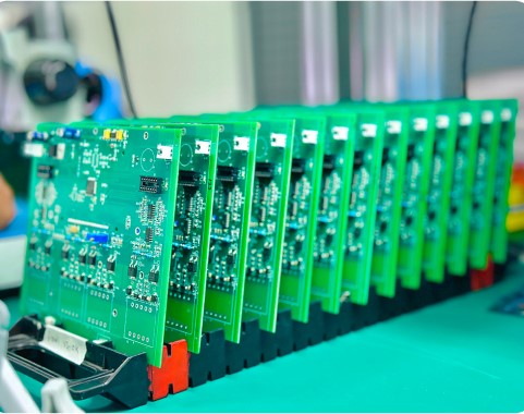
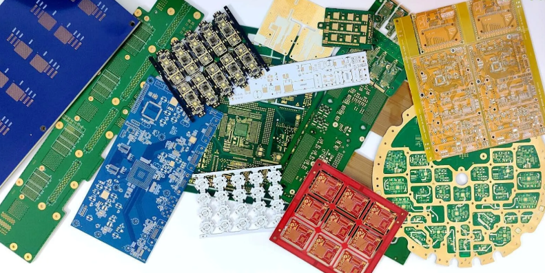
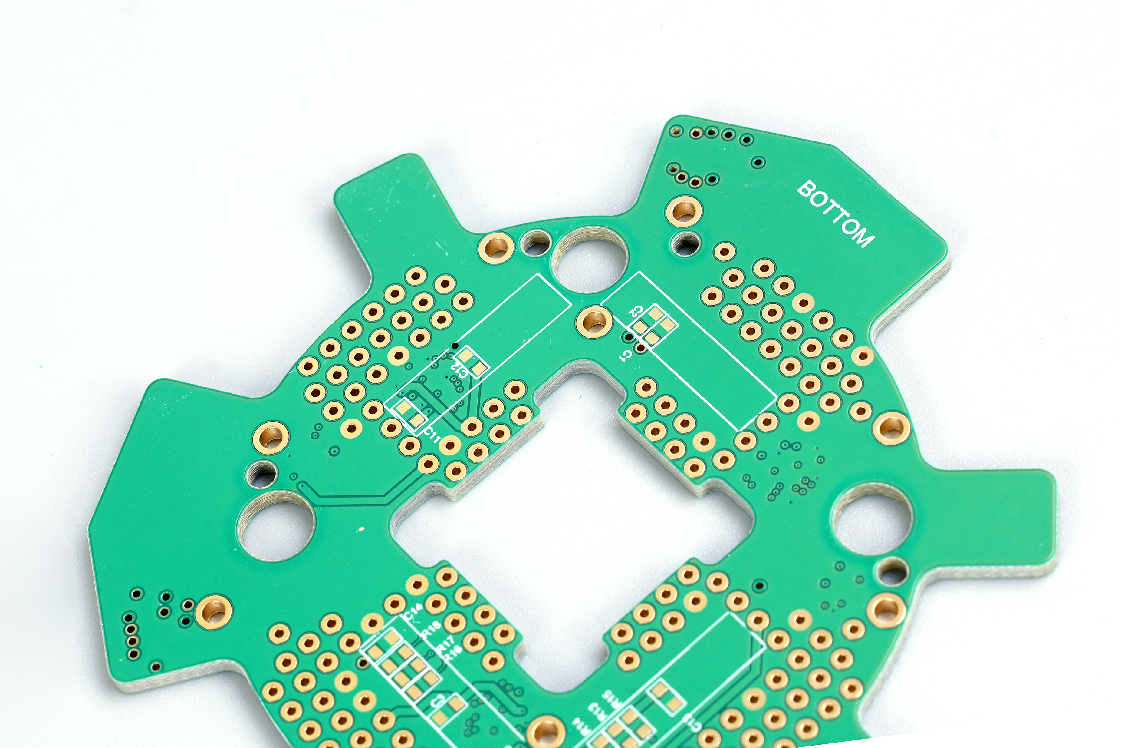
From a PCB manufacturing perspective, analog circuit vs digital circuit is not just a theoretical discussion about signal types. It directly affects stack-up design, component placement, grounding strategy, impedance control, EMI performance, and yield stability during fabrication and assembly.
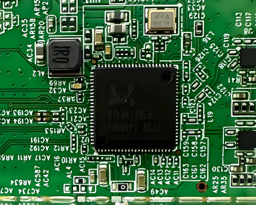
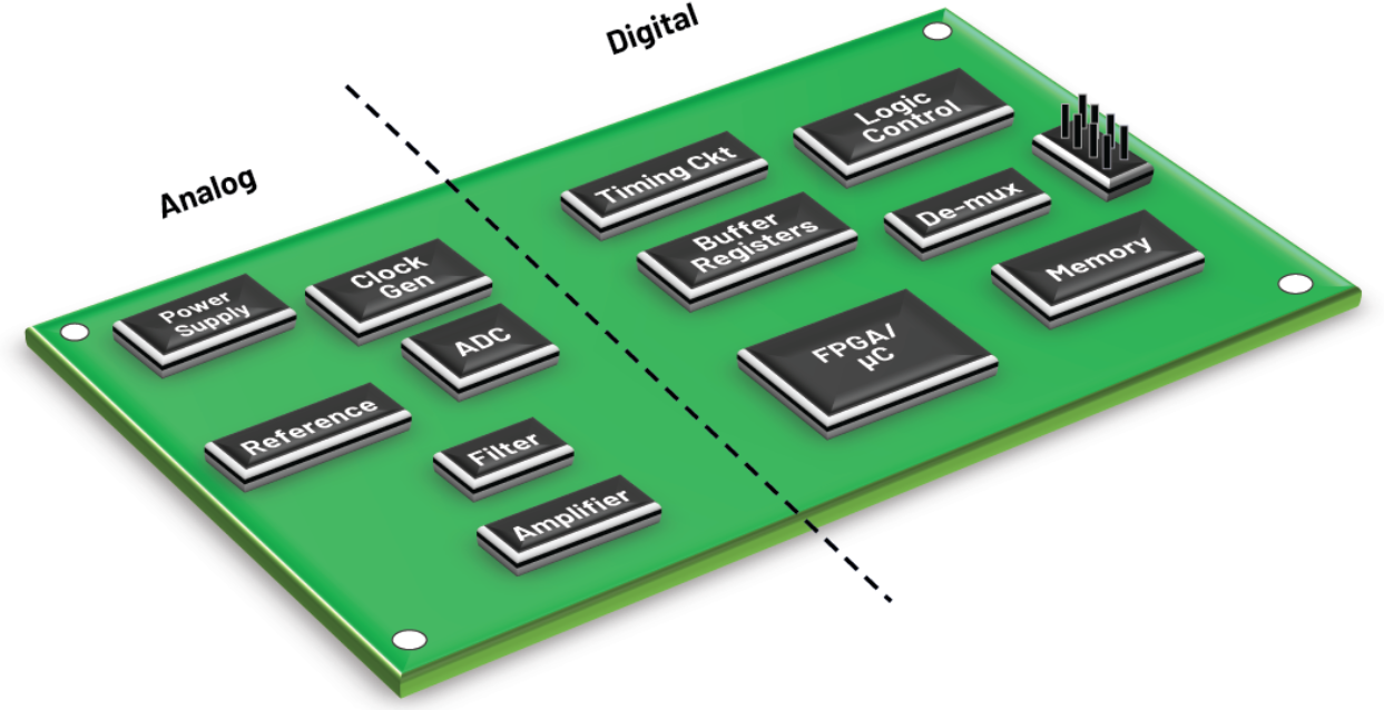
Most modern PCBs are mixed-signal boards, where analog and digital circuits coexist. Understanding how these two circuit types behave on a physical PCB is critical to achieving stable performance and high manufacturing reliability.

What Is an Analog Circuit?
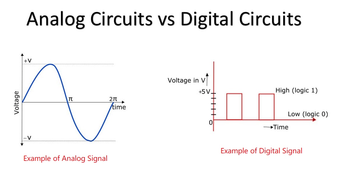
An analog circuit handles continuously varying electrical signals, which makes it inherently sensitive to layout parasitics, copper geometry, and material properties.
From a PCB standpoint, analog circuits are strongly influenced by:
- Trace impedance and length
- Parasitic capacitance and inductance
- Ground noise and return paths
- Dielectric consistency
Even small layout deviations can introduce offset, distortion, or noise coupling. As a result, analog PCB design places heavy emphasis on short signal paths, controlled grounding, and clean reference planes.
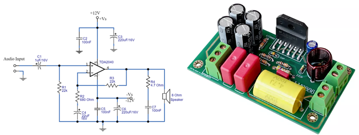
Analog Circuit Diagram and Typical PCB Layout
In analog PCB layouts, signal flow is often linear and localized. Components are placed close together to minimize loop area and external interference.
Key layout characteristics include:
- Compact placement of passive components
- Dedicated analog ground regions
- Minimal via usage in sensitive signal paths
For PCB manufacturers, tight analog layouts also demand accurate drilling, consistent copper thickness, and stable dielectric properties, especially for low-noise or high-gain designs.
What Is a Digital Circuit?
A digital circuit processes signals in discrete logic states, which makes it more tolerant of voltage variation but highly sensitive to timing, impedance, and reference integrity.
On a PCB, digital performance is driven by:
- Signal rise and fall times
- Controlled impedance routing
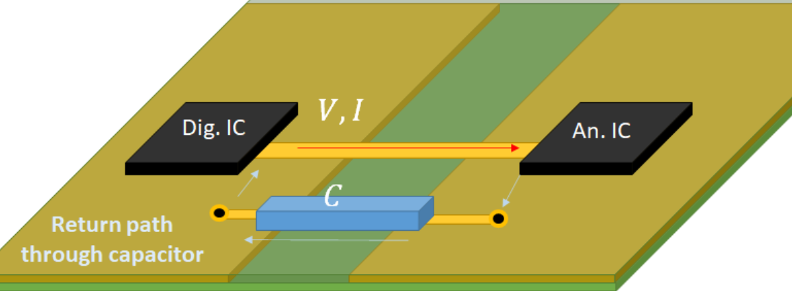
- Return current continuity
- Power distribution network stability
High-speed digital circuits can fail not because of logic errors, but because of poor PCB layout.
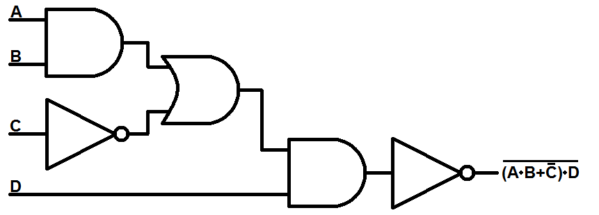
Digital Circuit Diagram and PCB Routing Rules
Digital PCB layouts emphasize structured routing and plane continuity rather than compact clustering.
Typical digital PCB features include:
- Wide, continuous ground planes
- Matched-length signal routing
- Decoupling capacitors placed at power pins
- Clear separation of clock and data paths
For fabrication, this often requires tight impedance control, consistent layer registration, and precise etching tolerances.
Analog and Digital Circuits Examples in PCB Manufacturing
Analog-dominant PCB examples:
- Sensor interface boards
- Audio processing PCBs
- Power feedback and control loops
- RF front-end circuits
Digital-dominant PCB examples:
- Microcontroller control boards
- FPGA and CPU modules
- Data acquisition systems
- Communication processing boards
In manufacturing reality, most products combine both. This mixed-signal nature creates layout and DFM challenges that must be addressed early.
What Is the Difference Between Analog and Digital Circuits on a PCB?
The fundamental difference appears in how signals interact with the PCB itself.
Analog circuits are affected by:
- Copper geometry
- Dielectric loss and consistency
- Crosstalk and EMI
Digital circuits are affected by:
- Impedance discontinuities
- Ground reference breaks
- Timing skew and reflection
Because of this, PCB manufacturers often recommend different layout rules, spacing, and plane strategies for analog and digital sections on the same board.
Analog Circuit vs Digital Circuit: Pros and Cons for PCB Manufacturing
Analog PCB advantages:
- Lower routing density
- Fewer high-speed constraints
- Simpler impedance requirements
Analog PCB challenges:
- High sensitivity to noise
- Performance variation due to material tolerances
- Greater dependence on layout discipline
Digital PCB advantages:
- Predictable logic behavior
- Easier functional testing
- Scalable designs
Digital PCB challenges:
- Tight impedance and stack-up control
- EMI and signal integrity risks
- Higher layer count requirements
These tradeoffs directly influence PCB cost, lead time, and yield stability.
Mixed-Signal PCB Layout: Key DFM Considerations
When analog and digital circuits share the same PCB, DFM becomes critical.
Best practices include:
- Physical separation of analog and digital sections
- Single-point ground connection strategy
- Separate power planes or filtered power domains
- Controlled return current paths
From a manufacturing view, mixed-signal boards benefit from:
- Clear net labeling
- Defined impedance rules
- Early DFM review to avoid late-stage redesign
Is HDMI Analog or Digital? Implications for PCB Design
HDMI is a fully digital interface, operating at high data rates with differential signaling.
For PCB fabrication, HDMI designs require:
- Tight differential impedance control
- Low-loss materials for longer traces
- Precise length matching
Even though HDMI is digital, poor PCB layout can quickly degrade signal integrity, reinforcing the importance of manufacturing expertise.
When Should PCB Designers Use Analog vs Digital Circuits?
From a PCB manufacturer’s perspective:
Use analog circuits when:
- Interfacing directly with sensors or transducers
- Precision signal conditioning is required
- Low latency is critical
Use digital circuits when:
- Data processing and control dominate
- Noise immunity is essential
- System scalability is required
In practice, successful products rely on well-partitioned mixed-signal PCB designs, supported by fabrication processes that can meet both analog stability and digital integrity requirements.
FAQs
1. Can analog and digital circuits be placed on the same PCB?
Yes. Most modern PCBs are mixed-signal designs. However, proper partitioning, controlled grounding, filtered power domains, and careful routing are required to prevent digital switching noise from degrading analog performance.
2. Do digital circuits really need impedance-controlled traces?
For low-speed digital circuits, impedance control may not be critical. For high-speed digital interfaces such as HDMI, USB, Ethernet, or DDR, controlled impedance is essential to prevent signal reflections, eye closure, and EMI issues.
3. What PCB materials are commonly used for analog and digital boards?
Standard FR-4 is widely used for both. However:
- Precision analog or RF designs may require tighter Dk/Df control
- High-speed digital designs may benefit from low-loss laminates
4. Why do digital systems still need analog circuits?
All digital systems interact with the real world through analog signals. Sensors, power regulation, clock generation, and signal inputs are inherently analog, making analog circuitry unavoidable even in fully digital products.
5. When should DFM review be done for mixed-signal PCBs?
DFM review should be done before layout finalization, ideally during stack-up planning. Early DFM feedback helps avoid impedance mismatches, grounding conflicts, via limitations, and fabrication constraints that are costly to correct later.