Why Choose EBest for Your Ceramic Substrate PCB Needs?
EBest stands as your premier choice for Ceramic Substrate PCB manufacturing and prototyping. We deliver unmatched lead times, rigorous quality control, industry-leading certifications, and comprehensive support throughout your project. Our commitment to excellence ensures your Ceramic Substrate PCB projects are completed efficiently, reliably, and to the highest standards.
- Fast Delivery: Industry-leading turnaround times for prototypes and mass production, meeting your critical project deadlines.
- Superior Quality: Precision manufacturing with zero-defect tolerance, ensuring optimal performance and long-term reliability.
- Certified Excellence: Compliant with ISO 9001, IPC-A-600, and other international quality and safety standards.
- Expert Support: A dedicated engineering team provides end-to-end technical assistance, from design to delivery.
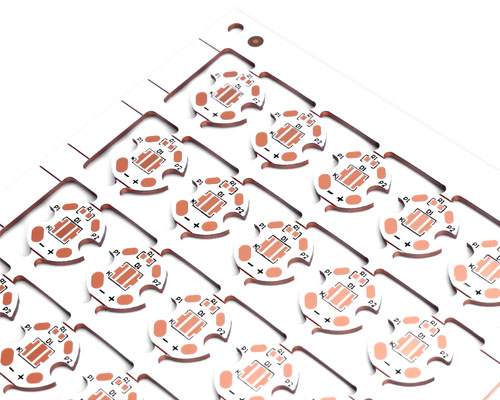
What is a Ceramic Substrate PCB?
A Ceramic Substrate PCB is a specialized printed circuit board that uses ceramic materials (such as alumina Al₂O₃, aluminum nitride AlN, or silicon nitride Si₃N₄) as its base insulating layer instead of traditional organic materials like FR-4. These boards are engineered to excel in high-temperature, high-power, and high-frequency electronic applications where standard PCBs fail. The ceramic substrate provides exceptional thermal conductivity, electrical insulation, and mechanical stability, making it indispensable for modern, demanding electronics.
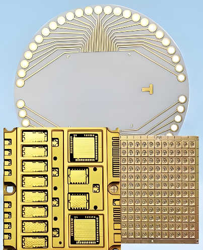
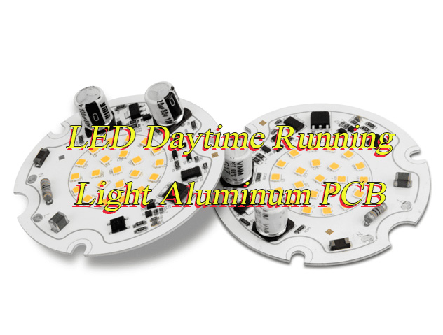
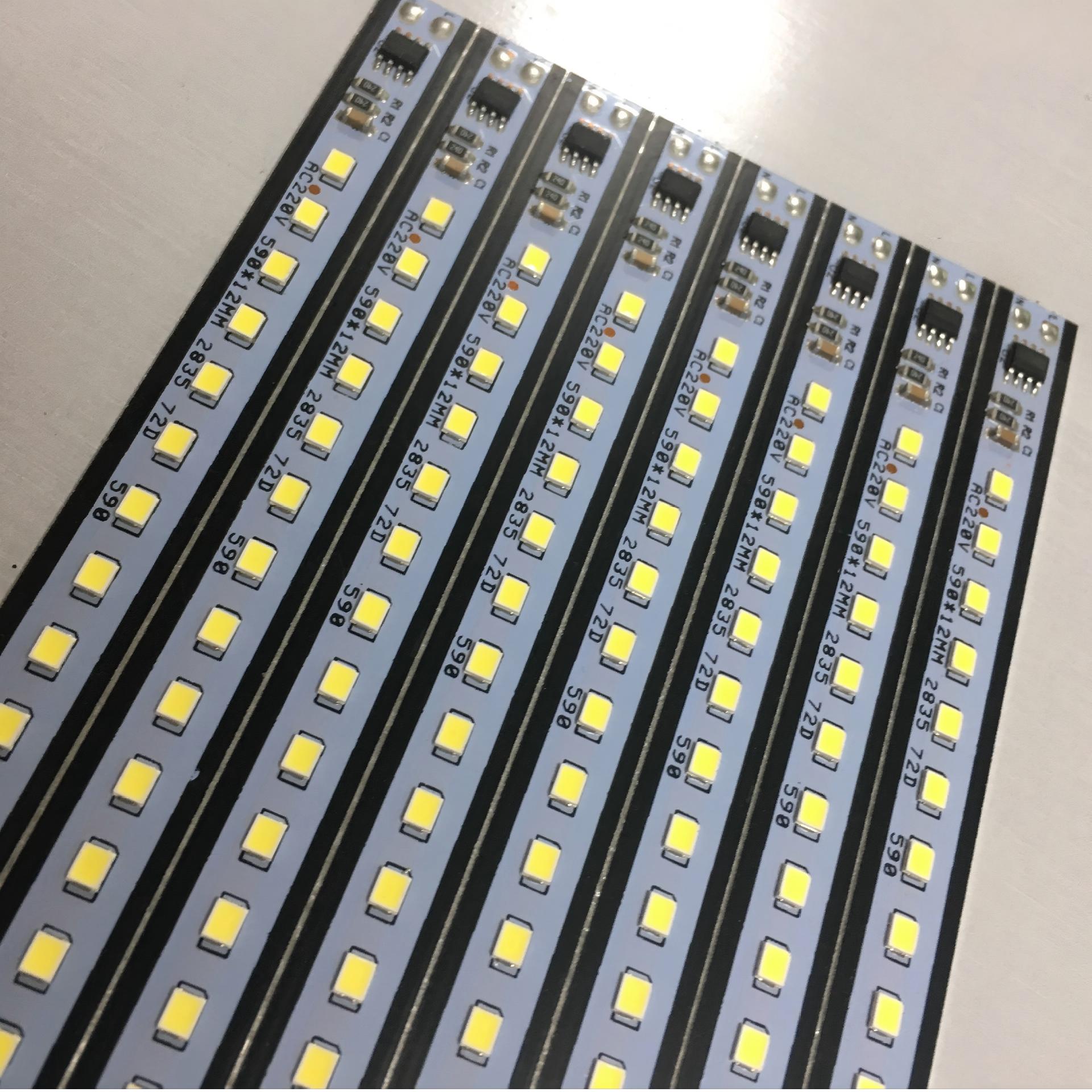
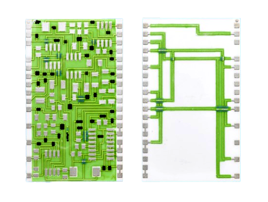
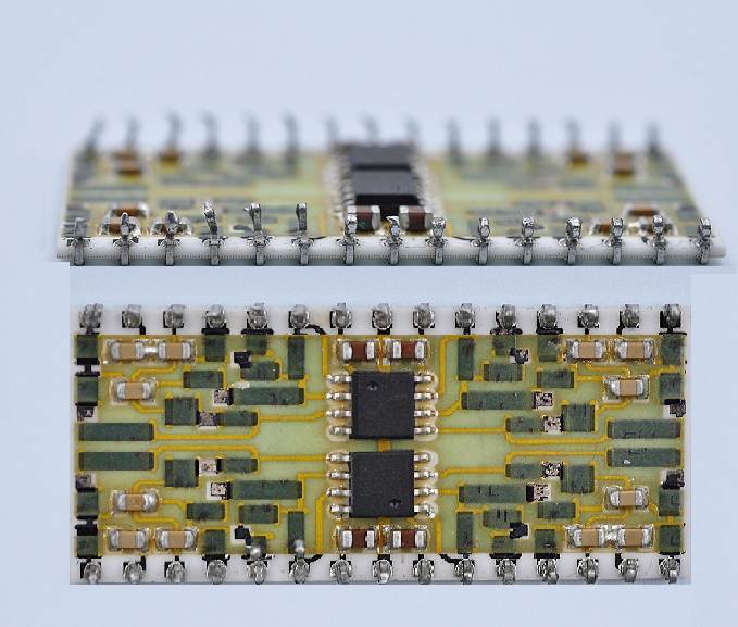
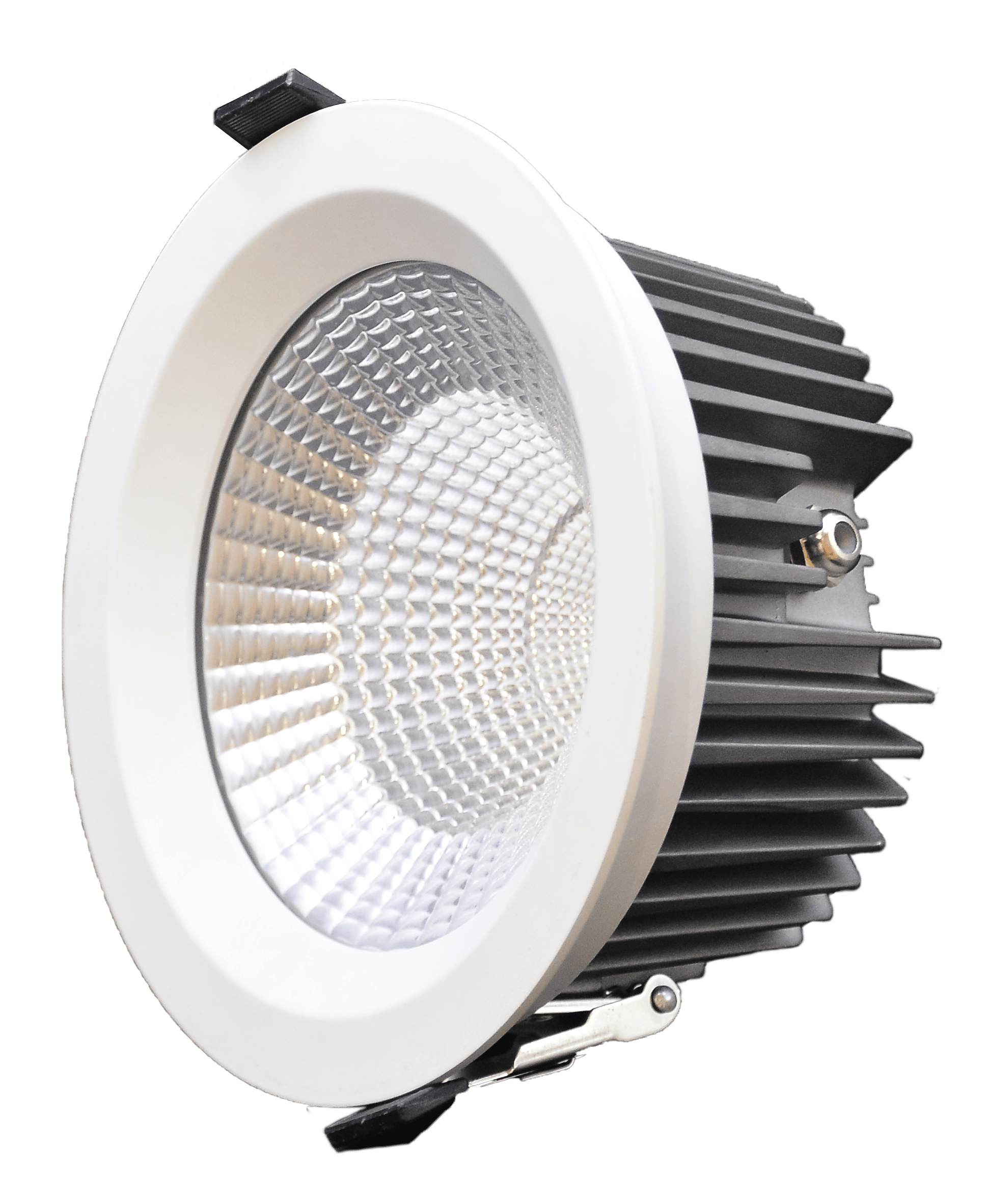
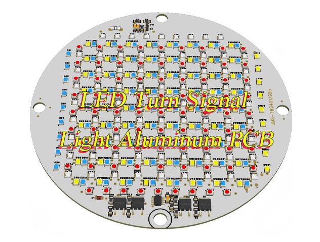
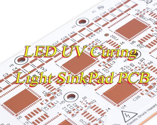
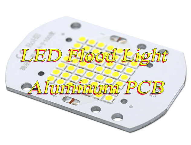
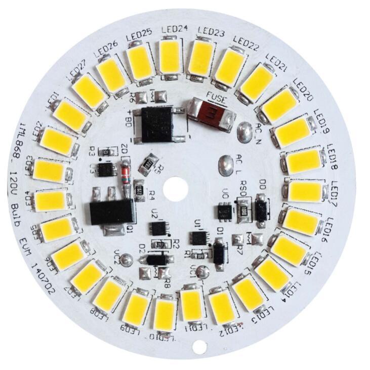
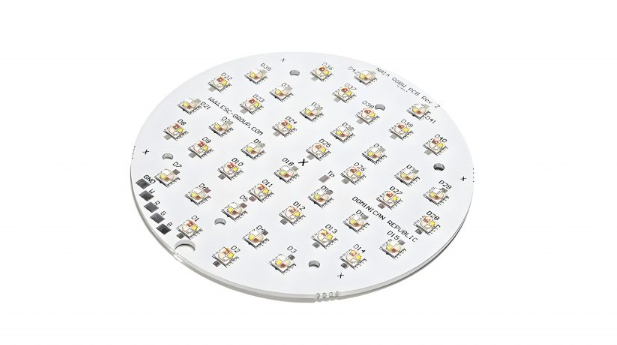
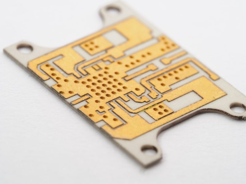
Ceramic Substrate PCB
Ceramic Substrate PCB Stackup
| Layer | Material | Thickness (Typical) | Function |
|---|---|---|---|
| Top Copper | Electrodeposited Copper | 1–5 oz (35–175 μm) | Conductive traces, pads, and planes |
| Ceramic Core | Alumina (Al₂O₃) / Aluminum Nitride (AlN) | 0.25–2.0 mm | Insulation, thermal management, structural support |
| Bottom Copper | Electrodeposited Copper | 1–5 oz (35–175 μm) | Conductive traces, pads, and planes |
| Surface Finish | ENIG / Immersion Silver / OSP | 0.05–0.5 μm | Protect copper, improve solderability |
Note: Multilayer ceramic substrate PCBs (LTCC/HTCC) feature alternating ceramic and conductive layers, typically up to 10–20 layers for high-density integration.
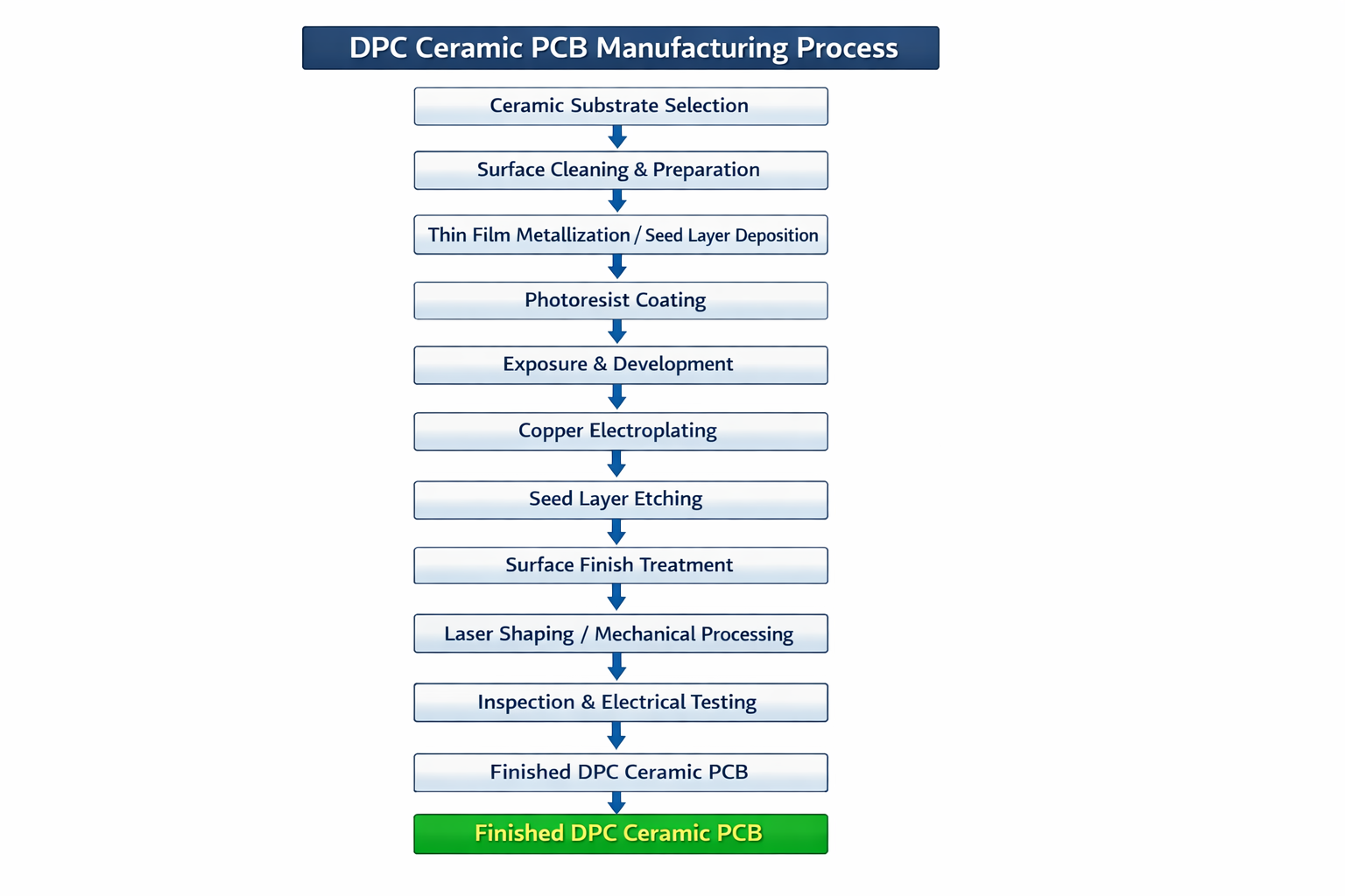
Ceramic Substrate PCB Manufacturing Process
Step 1: Ceramic Substrate Preparation
High-purity ceramic powders (Al₂O₃, AlN) are pressed into green sheets, precisely cut to size, and sintered at ultra-high temperatures (1,600–1,800°C) to form dense, rigid substrates with consistent material properties.
Step 2: Metallization & Circuit Patterning
Copper is bonded to the ceramic surface using advanced processes:
- DBC (Direct Bonded Copper): Copper foil is fusion-bonded to ceramic at ~1,065°C.
- DPC (Direct Plated Copper): Copper is electroplated onto a sputtered seed layer for fine-line precision.
Photolithography and etching define the circuit pattern, creating high-resolution traces and pads.
Step 3: Via Formation & Plating
Micro-vias are created using laser drilling for precision. The via walls are metallized through electroplating to establish vertical electrical connections between layers, critical for thermal and signal paths.
Step 4: Surface Treatment & Finishing
The board undergoes surface finishing (ENIG, immersion silver, etc.) to protect the copper circuitry and ensure reliable solderability during component assembly.
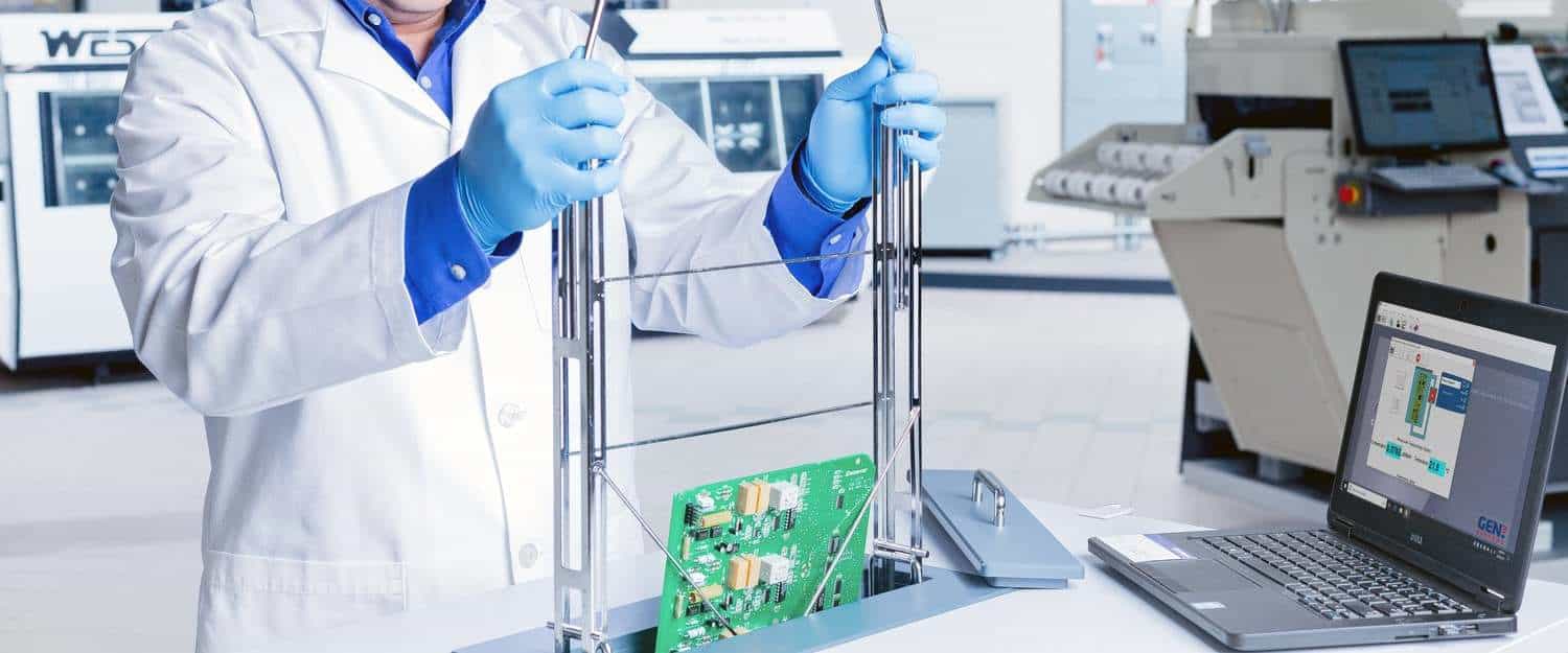
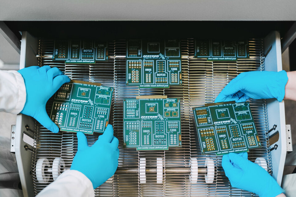
Step 5: Testing & Quality Assurance
Each Ceramic Substrate PCB undergoes rigorous electrical testing (continuity, insulation resistance), thermal cycling, and visual inspection to guarantee compliance with specifications and performance standards.
Ceramic Substrate PCB Design Guide
Designing a Ceramic Substrate PCB requires specialized knowledge to overcome inherent material challenges. Key pain points include material brittleness, CTE mismatch with components, thermal management, and fine-line manufacturing constraints. EBest’s engineering team provides expert guidance to navigate these challenges and optimize your design for success.
Key Design Considerations & Solutions
Material Compatibility & CTE Matching
- Pain Point: A significant CTE mismatch between ceramic (5–7 ppm/°C) and silicon (4.5 ppm/°C) causes thermal stress, leading to solder joint fatigue and substrate cracking.
- Solution: Select AlN (CTE ~4.5 ppm/°C) for silicon-based high-power devices. Use compliant materials and underfill in assembly to absorb stress.
Thermal Management Optimization
- Pain Point: Inefficient heat dissipation leads to hotspots and component failure in high-power designs.
- Solution: Maximize copper thickness in power paths, integrate thermal vias, and use large copper planes for heat spreading. AlN substrates offer 8–10x higher thermal conductivity than alumina.
Mechanical Stress & Fragility
- Pain Point: Ceramic brittleness causes chipping and cracking during handling, assembly, or thermal cycling.
- Solution: Avoid sharp corners; use rounded geometries. Design generous tolerances (+/–0.1 mm) and avoid V-cuts. Use robust panelization with thick connecting tabs.
Fine-Line & High-Density Design
- Pain Point: Achieving fine line widths/spacing (<50 μm) is challenging with standard processes.
- Solution: Utilize DPC technology for line widths down to 15 μm. Collaborate with EBest early for DFM analysis to ensure design manufacturability.
For flawless Ceramic Substrate PCB design, partner with EBest. Our experts provide complimentary DFM reviews and design optimization to ensure your project is built for performance and reliability.
Ceramic Substrate PCB Prototype: Rapid, Reliable, Custom
Prototyping Ceramic Substrate PCBs presents unique hurdles: long lead times, high costs, and difficulty in achieving consistent quality with low volumes. EBest specializes in rapid, high-quality Ceramic Substrate PCB prototyping, eliminating these barriers and accelerating your product development cycle.
Prototype Challenges & Our Solutions
Long Lead Times for Custom Prototypes
- Challenge: Traditional ceramic PCB prototyping can take weeks, delaying product validation.
- Solution: EBest offers rapid prototype services with industry-leading turnaround times, getting your boards in hand quickly.
High Cost for Low-Volume Runs
- Challenge: High tooling and setup costs make small-batch prototyping prohibitively expensive.
- Solution: We maintain flexible manufacturing lines optimized for low-volume, high-mix production, keeping prototype costs competitive.
Inconsistent Prototype Quality
- Challenge: Achieving the same material and process quality in prototypes as in mass production is difficult.
- Solution: Our prototypes use the exact same materials and production processes as full-scale manufacturing, ensuring reliable performance data.
Limited Design Iteration
- Challenge: Cost and time constraints limit the number of design iterations possible.
- Solution: Our efficient prototyping process allows for multiple design iterations, enabling you to refine and perfect your design before full production.
Trust EBest for your Ceramic Substrate PCB prototyping needs. We deliver fast, affordable, and production-quality prototypes to validate your design and accelerate your time-to-market.
How to Choose Ceramic Substrate PCB Raw Materials
Selecting the right ceramic material is critical for balancing performance, cost, and application suitability. The table below compares the most common materials:
| Material | Thermal Conductivity (W/m·K) | CTE (ppm/°C) | Dielectric Constant (εr) | Key Applications |
|---|---|---|---|---|
| Alumina (96% Al₂O₃) | 20–25 | ~7.0 | 9.5 | Consumer electronics, industrial control, LED lighting |
| Alumina (99% Al₂O₃) | 28–30 | ~7.0 | 9.8 | Automotive electronics, medical devices, telecom |
| Aluminum Nitride (AlN) | 170–230 | ~4.5 | 8.8 | High-power semiconductors, RF, EV power modules |
| Silicon Nitride (Si₃N₄) | 80–100 | ~3.2 | 7.8 | Automotive, aerospace, high-reliability industrial |
Ceramic Substrate PCB Applications
Ceramic Substrate PCBs are the backbone of high-performance electronics across critical industries, enabling innovation where thermal, electrical, and reliability demands are extreme.
Automotive Electronics
Ceramic Substrate PCBs are essential in electric vehicle (EV) powertrains, including IGBT modules, on-board chargers (OBC), and LED headlight drivers. They withstand extreme under-hood temperatures (-40°C to 150°C) and provide superior thermal management for high-voltage, high-power systems.
Communication & 5G Infrastructure
In 5G base stations, RF power amplifiers, and microwave systems, Ceramic Substrate PCBs (especially AlN) offer low dielectric loss and excellent thermal stability, ensuring signal integrity and efficient heat dissipation for high-frequency, high-power operation.
Industrial Automation & Power Electronics
Used in variable-frequency drives (VFDs), servo controls, and power supplies, these boards handle high power densities and harsh industrial environments. Their excellent thermal conductivity and mechanical strength ensure reliable operation in continuous-duty applications.
Medical Devices
Ceramic Substrate PCBs are used in precision medical equipment like ultrasound systems, patient monitors, and surgical lasers. They offer biocompatibility, high electrical insulation, and the ability to withstand repeated sterilization cycles, meeting strict medical device standards.
What Are the Key Advantages of Ceramic Substrate PCB Over FR4?
Ceramic Substrate PCBs offer transformative advantages over traditional FR-4 PCBs, particularly in high-performance applications. Key benefits include:
- Superior Thermal Conductivity: Up to 1,000x higher than FR-4, enabling efficient heat dissipation.
- Excellent Electrical Insulation: High dielectric strength prevents short circuits in high-voltage applications.
- Extreme Temperature Resistance: Operates reliably from -50°C to over 350°C.
- Mechanical Stability: High rigidity and resistance to warping under thermal stress.
- Chemical Inertness: Resistant to most chemicals, ideal for harsh environments.
How Does Thermal Conductivity Impact Ceramic Substrate PCB Performance?
Thermal conductivity is the defining performance metric for Ceramic Substrate PCBs. It directly determines the board’s ability to dissipate heat generated by power components. Higher thermal conductivity (e.g., AlN at 200 W/m·K vs. alumina at 25 W/m·K) allows for:
- Higher power density designs in smaller form factors.
- Lower component operating temperatures, significantly increasing reliability and lifespan.
- Elimination of bulky heat sinks, enabling more compact and efficient product designs.
What Are the Common Failure Modes in Ceramic Substrate PCBs?
The primary failure modes stem from thermal and mechanical stress:
- Thermal Fatigue: CTE mismatch causes cyclic stress, leading to solder joint cracking or substrate delamination.
- Mechanical Fracture: Brittleness leads to cracking from shock, vibration, or improper handling.
- Metallization Degradation: Oxidation or poor adhesion of the copper layer causes open circuits.
- Thermal Runaway: Inadequate heat dissipation leads to overheating and catastrophic failure.
Can Ceramic Substrate PCBs Be Used for High-Frequency Applications?
Absolutely. Ceramic Substrate PCBs, especially AlN and high-purity alumina, are ideal for high-frequency (RF/microwave) applications. They offer:
- Low Dielectric Loss (tan δ): Minimizes signal attenuation and power loss.
- Stable Dielectric Constant: Ensures consistent signal propagation across temperature variations.
- Excellent High-Frequency Performance: Supports frequencies up to mmWave bands for 5G and radar systems.
What Is the Difference Between DBC and DPC Ceramic Substrate PCB?
DBC (Direct Bonded Copper) and DPC (Direct Plated Copper) are the two primary manufacturing technologies:
- DBC: Copper foil is fusion-bonded to ceramic at high temperature. It is best for thick copper (up to 10 oz) and high-power applications. It offers excellent thermal performance but limited line resolution (~100 μm).
- DPC: Copper is electroplated onto a sputtered seed layer. It enables ultra-fine line widths (<15 μm) for high-density, high-frequency designs. It is ideal for complex, miniaturized circuits.
Ceramic Substrate PCB FAQ
Q1: What is the maximum operating temperature for a Ceramic Substrate PCB?
A1: Ceramic Substrate PCBs can reliably operate at continuous temperatures up to 350°C, with short-term peaks exceeding 500°C—far exceeding the limits of FR-4.
Q2: Can you manufacture flexible Ceramic Substrate PCBs?
A2: While inherently rigid, specialized ceramic composites and LTCC (Low-Temperature Co-fired Ceramic) technologies can produce semi-flexible or 3D-shaped Ceramic Substrate PCBs for specific applications.
Q3: What is the minimum line width/spacing achievable?
A3: Using DPC technology, EBest can achieve line widths and spacing as fine as 15 μm, enabling high-density circuit designs.
Q4: Are Ceramic Substrate PCBs suitable for mass production?
A4: Yes. EBest operates automated production lines capable of high-volume, consistent manufacturing of Ceramic Substrate PCBs for industrial and automotive applications.
Q5: How do I get a quote for my Ceramic Substrate PCB project?
A5: Contact our sales team with your Gerber files, BOM, layer stackup, quantity, and target delivery date. We provide detailed, competitive quotes quickly.
Q6: What surface finishes are available for Ceramic Substrate PCBs?
A6: We offer ENIG (Electroless Nickel Immersion Gold), immersion silver, and OSP (Organic Solderability Preservative) to meet various assembly and reliability requirements.
Q7: Can you assemble components on Ceramic Substrate PCBs?
A7: Yes, EBest provides full turnkey services, including high-precision SMT and through-hole component assembly for Ceramic Substrate PCBs.
Ready to Start Your Ceramic Substrate PCB Project?
EBest is your trusted partner for all Ceramic Substrate PCB design, prototyping, and manufacturing needs. With our technical expertise, fast delivery, and commitment to quality, we ensure your project succeeds. Contact us today to discuss your requirements and get a free quote.
Email: sales@bestpcbs.com