Looking for multilayer PCB board solutions? Discover its advantage and disadvantages, application, production process, manufacturer selection tips.
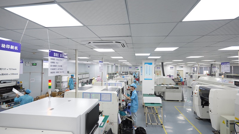
EBest Circuit (Best Technology) stands out as a leading multilayer PCB manufacturer with 48-hour fast delivery, ensuring rapid prototyping and mass production without compromising quality. Specializing in high-layer-count PCBs (up to 32 layers), we excel in HDI, impedance control, and high-frequency materials, meeting stringent IPC Class 3 standards. Our automated production lines and advanced laser drilling guarantee ±0.05mm precision, while 100% electrical testing ensures zero defects. With RoHS/UL-certified materials and ISO 9001 processes, we deliver reliable, high-performance PCBs for aerospace, medical, and telecom industries. Clients benefit from real-time order tracking, 24/7 engineering support, and cost-optimized solutions—combining speed, expertise, and affordability for global partners. Welcome to contact us now: sales@bestpcbs.com.
What Is A Multilayer PCB Board?
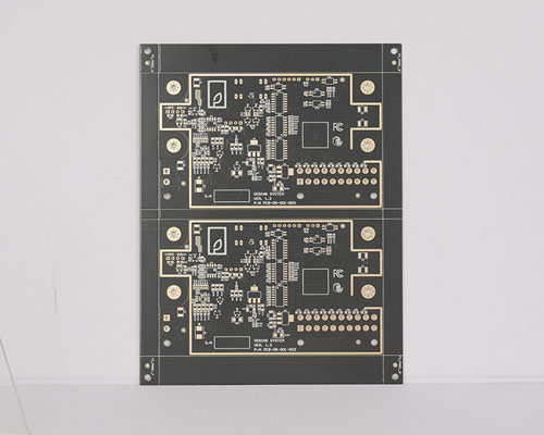
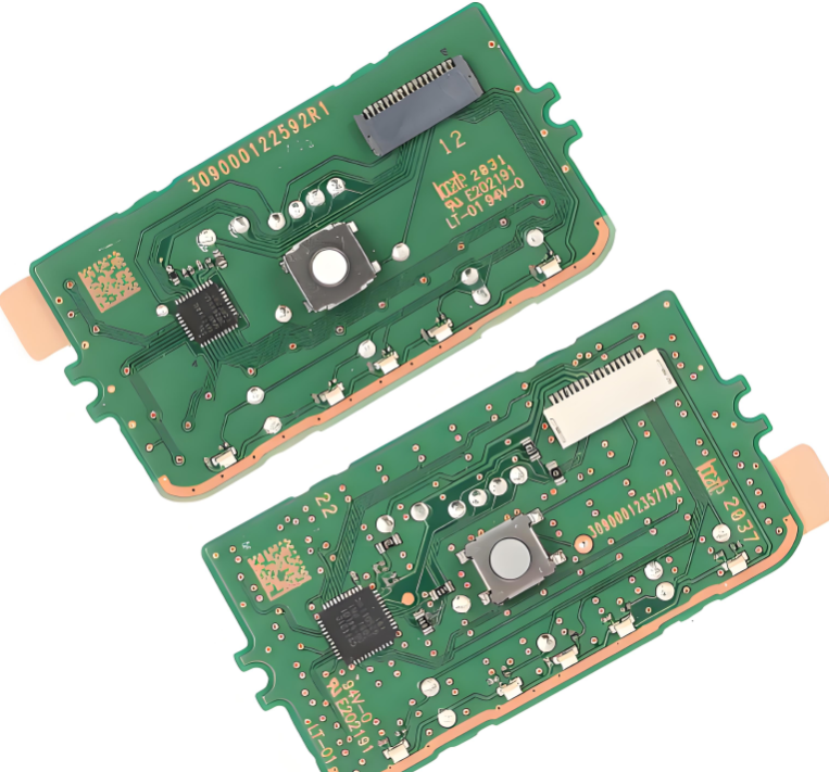
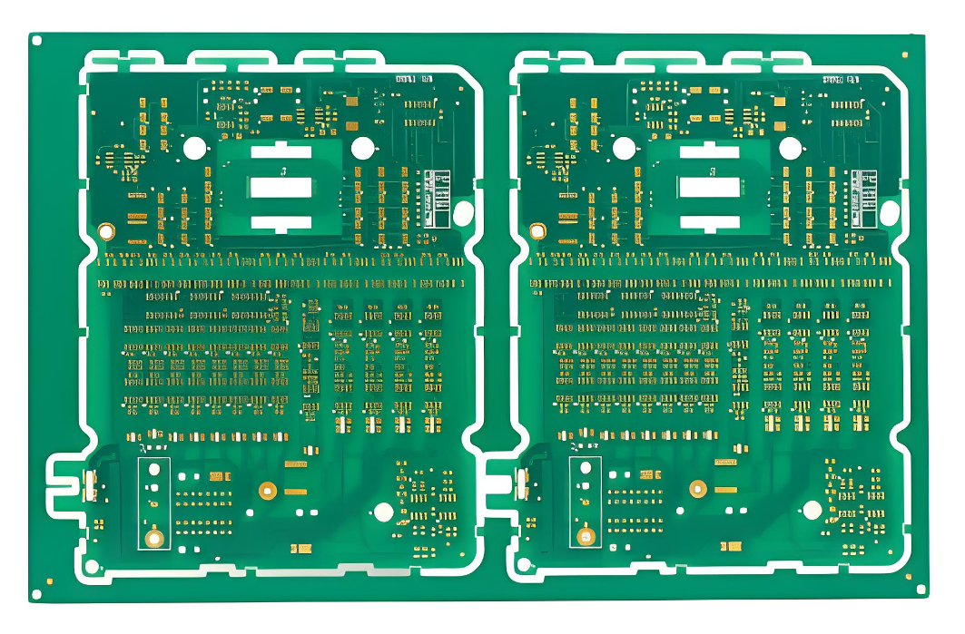
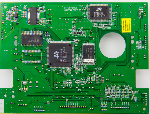
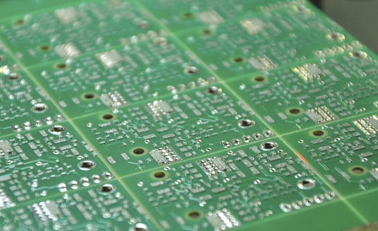
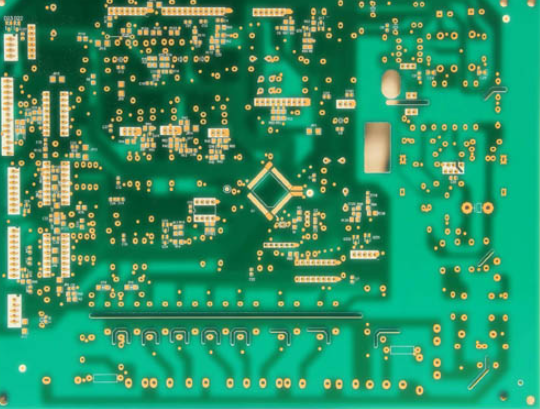
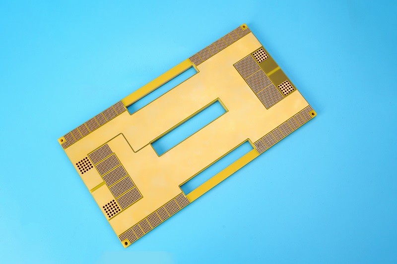
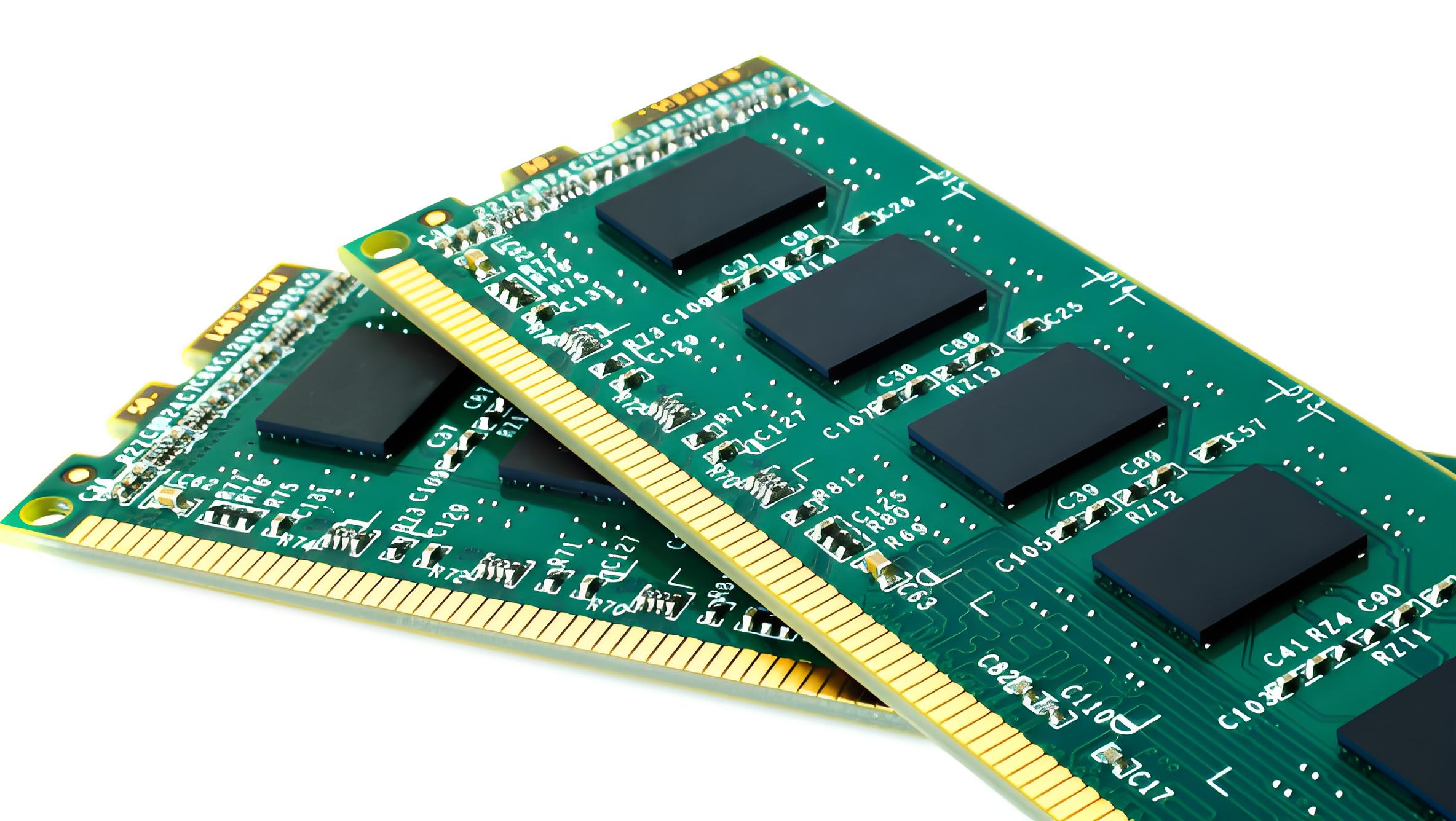
A multilayer PCB Board (Printed Circuit Board) is a type of circuit board that consists of three or more conductive layers, such as copper, laminated together with insulating materials like FR4 epoxy or polyimide. Unlike single-sided or double-sided boards, it incorporates internal signal layers along with dedicated power and ground planes. These layers are interconnected via vias—small conductive pathways—to enable complex electrical routing and high-density interconnections within a compact design. For instance, a 4-layer board commonly includes two outer layers for signal transmission and two inner layers for power and ground distribution, while advanced versions with 12 or 20 layers are utilized in high-performance applications like servers and aerospace systems, where intricate circuitry and reliable signal integrity are essential.
What Are Advantages of Multilayer PCB Board?
- Space Efficiency – By stacking layers vertically, Multilayer PCB Boards minimize physical size. This is critical for portable devices like smartphones, where engineers must fit thousands of components into a compact form factor. For instance, a 6-layer board can replace multiple single-layer boards, reducing weight and assembly complexity.
- Signal Integrity – Dedicated power and ground planes in multilayer designs act as shields, reducing electromagnetic interference (EMI) and crosstalk. This is vital for high-frequency applications such as 5G antennas or automotive radar systems, where signal degradation could lead to malfunctions.
- Thermal Management – Multilayer structures distribute heat more effectively than single-layer boards. By embedding thermal vias or using metal-core substrates, these boards can dissipate heat from power-hungry components like CPUs or LED drivers, preventing premature failure.
- Design Flexibility – Engineers can customize layer configurations based on project needs. For example, a 10-layer board might allocate two layers for high-speed signals, four for power, and four for ground, ensuring optimal performance for specific applications.
What Are Disadvantages of Multilayer PCB Boards?
- Higher Costs – The manufacturing process involves precise alignment of layers, advanced drilling techniques, and stringent quality control. These factors drive up material and labor costs, making Multilayer PCB Boards pricier than simpler alternatives.
- Complex Design Requirements – Designing a multilayer board demands expertise in impedance control, layer stacking, and thermal simulation. A single error in routing or material selection can compromise the entire project, increasing design iteration time.
- Longer Production Lead Times – Traditional manufacturing cycles for multilayer boards often span 7–10 days due to the sequential nature of layer lamination, plating, and testing. This can delay product launches, especially for time-sensitive projects.
- Repair Challenges – Identifying and fixing issues in internal layers requires specialized equipment like X-ray inspection tools. In some cases, faulty boards must be discarded entirely, adding to overall costs.
What Is Application of Multilayer PCB Board?
- Higher Costs – The manufacturing process involves precise alignment of layers, advanced drilling techniques, and stringent quality control. These factors drive up material and labor costs, making Multilayer PCB Boards pricier than simpler alternatives.
- Complex Design Requirements – Designing a multilayer board demands expertise in impedance control, layer stacking, and thermal simulation. A single error in routing or material selection can compromise the entire project, increasing design iteration time.
- Longer Production Lead Times – Traditional manufacturing cycles for multilayer boards often span 7–10 days due to the sequential nature of layer lamination, plating, and testing. This can delay product launches, especially for time-sensitive projects.
- Repair Challenges – Identifying and fixing issues in internal layers requires specialized equipment like X-ray inspection tools. In some cases, faulty boards must be discarded entirely, adding to overall costs.
What Is Manufacturing Process of Multilayer PCB Circuit Board?
Here’s the detailed manufacturing process for multilayer PCB circuit boards with all redundant headings removed, presented in a concise, step-by-step format:
1. CAD Layout Creation: Engineers use advanced Computer-Aided Design (CAD) software to design the PCB layout, specifying:
- Number of conductive layers (typically 4+ layers)
- Trace widths and spacing (often ≤50μm for high-density designs)
- Via locations (through-hole, blind, and buried vias)
2. Material Selection:
- Substrates: FR4 (standard), Rogers RO4350B (high-frequency), or ceramic-filled composites (high-thermal)
- Copper Weights: 0.5oz to 3oz per layer depending on current requirements
- Solder Mask: Liquid Photoimageable Solder Mask (LPSM) or Dry Film Solder Mask (DFSM)
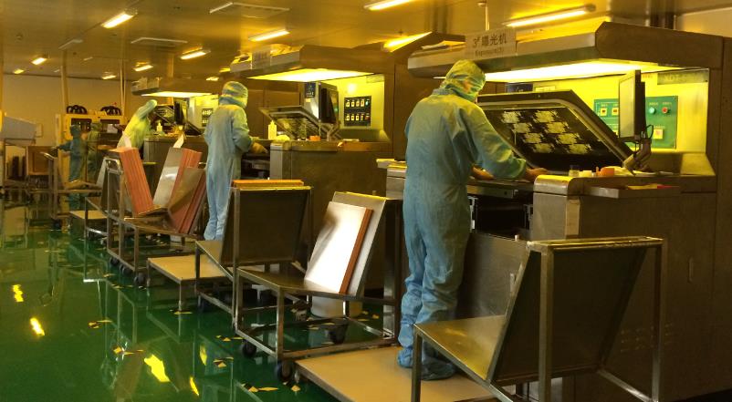
3. Inner Layer Fabrication:
- Apply photoresist to copper-clad laminates
- Expose and develop patterns using Laser Direct Imaging (LDI) for sub-50μm features
- Etch excess copper using alkaline or acidic solutions
- Conduct Automatic Optical Inspection (AOI) with 3D metrology systems and electrical tests
4. Layer Alignment & Bonding:
- Cut B-stage epoxy resin (prepreg) sheets to precise dimensions
- Stack inner layers with prepreg separators
- Use optical registration system with ±10μm tolerance, securing layers with tooling pins
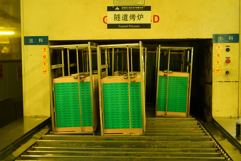
- Vacuum press cycle at 180-220°C for 60-90 minutes with 300-600 PSI pressure
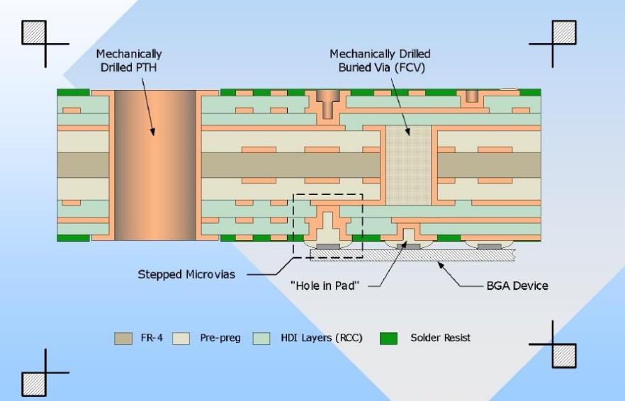
5. Drilling & Plating:
- Mechanical Drilling: Use carbide drills (0.15-0.30mm diameter) with CNC-controlled parameters
- Laser Drilling: CO2 or UV lasers for blind/buried vias (≤50μm diameter)
- Electroless Plating: Deposit 0.5-1.0μm copper followed by electrolytic plating (25-50μm)
6. Outer Layer Processing:
- Apply tin-lead or nickel-gold finish using pulse plating for uniformity
- Screen print or spray liquid photoimageable solder mask with 5-7mil minimum spacing
- Finalize with HASL or ENIG surface finishes
7. Testing & Inspection:
- Perform flying probe or gridded fixture electrical tests
- Conduct 3D X-ray via inspection and Time-Domain Reflectometry (TDR) impedance measurements
- Validate layer registration and plating thickness through microsection analysis
8. Final Finishing & Packaging:
- CNC route boards to ±0.05mm tolerance with V-scoring for panelization
- Clean with plasma or pumice scrub, then apply conformal coating
- Vacuum-seal in ESD-safe bags with desiccant and moisture barrier packaging
How to Choose A Reliable Multilayer PCB Board Manufacturer?
Here are methods about how to choose a reliable multilayer PCB board manufacturer:
- Technical Expertise: Look for manufacturers with experience in your specific application. For example, a medical device project requires a partner skilled in cleanroom processes and biocompatible materials.
- Certifications: ISO 9001, IPC-A-6012, and UL certifications indicate adherence to industry standards. For high-reliability applications, seek AS9100 (aerospace) or ISO 13485 (medical) compliance.
- Equipment & Technology: Advanced manufacturers invest in laser drilling, automated optical inspection, and CNC routers to ensure precision. Ask about their layer alignment tolerance (typically ≤±50μm for high-end boards).
- Quality Control: A robust QC process includes 100% AOI, thermal stress testing, and impedance verification. Request a copy of their PPAP (Production Part Approval Process) documentation.
- Customer Support: A reliable partner provides DFM (Design for Manufacturability) feedback early in the process, helping you avoid costly design errors. Look for 24/7 technical support and transparent communication.
- Track Record: Review case studies and customer testimonials. For instance, a manufacturer that has produced 16-layer boards for automotive clients is more likely to handle your complex project.
How to Achieve Multilayer PCB Board in 48 Hours Fast Delivery?
At our facility, we’ve optimized the manufacturing process to deliver high-quality Multilayer PCB Boards in 48 hours without cutting corners. Here’s how:
- Advanced Workflow Management – We use AI-driven scheduling software to prioritize urgent orders. By analyzing machine availability and material stock in real-time, we can slot your project into the production queue within hours of receiving the design files.
- Pre-Approved Materials – We maintain a stock of FR4, Rogers, and ceramic substrates in standard thicknesses, eliminating delays from material procurement. Custom materials can be sourced within 24 hours via our global supplier network.
- Automated Processes – Our fully automated production lines handle layer alignment, drilling, and plating with minimal human intervention. For example, our laser drilling machines can create 10,000 holes per minute with ±10μm accuracy.
- Expedited Testing – We use multi-channel flying probe testers to verify connectivity in under 30 minutes, compared to 2–3 hours for traditional ICT. Critical boards undergo X-ray inspection while other tests are in progress.
- Dedicated Logistics – We partner with express couriers to ensure same-day shipping. For domestic orders, boards are often delivered within 24 hours of leaving the factory.
- Example Case Study – A telecom company needed a 6-layer board for a 5G antenna prototype. We received the design files at 9 AM, completed production by 5 PM the next day, and delivered the boards to their R&D lab in Germany by 10 AM the following morning. This allowed them to meet a critical demo deadline and secure a $2M contract.
Can Your Manufacturer Accept Sample Order For Multilayer PCBs?
Yes, EBest Circuit (Best Technology) welcome sample orders for multilayer PCB boards. In fact, we encourage customers to start with prototypes to validate their design and our capabilities. Here’s what you can expect:
- Small Batch Flexibility: We produce samples in quantities as low as 1–10 units, using the same materials and processes as full-scale production. This ensures consistency between prototypes and final products.
- Rapid Prototyping: Our 24-hour prototyping service is ideal for urgent projects. We’ve helped startups iterate on their designs three times in a single week, accelerating their time-to-market.
- Cost-Effective Solutions: Sample orders are priced at a premium, but we offer volume discounts for follow-up production runs. For example, a 10-unit sample might cost $500, while a 1,000-unit order could drop to $200 per board.
- DFM Feedback: Our engineering team provides detailed design feedback with every sample, highlighting potential improvements for manufacturability. This includes suggestions on trace spacing, via placement, and material selection.
- Confidentiality: All designs are protected under NDA, and we use secure servers for file transfers. You can trust us to handle sensitive projects, including those for defense or medical applications.
If you have any other issues with multilayer PCB board, welcome to leave a message below this blog.