A lasercut stencil offers precision and customization like no other. But can a laser cutter make stencils? The answer is a resounding yes! Laser cutting technology has revolutionized stencil creation, providing industries with highly accurate, durable, and customizable stencils. Whether for screen printing, PCB manufacturing, or artistic projects, a laser cutter is an excellent tool for making a laser cut stencil.
Can Laser Cutters Make Stencils?
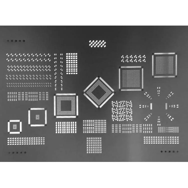
Yes, laser cutters are perfect for making stencils. Using focused laser beams, they cut through materials like mylar, plastic, and metal with incredible precision, offering sharp, clean edges that traditional methods can’t match. This makes them ideal for producing laser cut stencils for everything from screen printing to PCB manufacturing.
One of the biggest advantages of using a laser cutter is the level of detail it can achieve. Whether you need custom laser cut stencils for complex designs or laser cut stencils for painting, the technology ensures accuracy with tight tolerances, often as precise as ±4 μm. This reduces errors and ensures consistency across multiple stencils.
Additionally, laser cutters work with a variety of materials, such as mylar stencil sheets for screen printing or stainless steel for SMT stencils, giving you flexibility to choose the best material for your project. Laser cutting is efficient, saving time and minimizing the potential for mistakes compared to traditional methods.
Can You Make Stencils with a Laser Printer?
Laser printers and laser cutters might sound similar, but they serve different functions. While a laser printer uses toner and heat to print designs onto paper or other materials, a laser cutter uses focused laser beams to cut through materials such as plastic, metal, or mylar. So, can you make stencils with a laser printer? Not exactly. A laser cutter offers far more flexibility and precision, allowing you to create intricate designs on various materials, including the popular mylar stencil sheets used in screen printing.
Laser cutting not only makes sharper cuts but also works with a broader range of materials. From custom laser cut stencils for industrial use to laser cut stencils for painting and other crafts, the laser cutter is an essential tool for creating high-quality stencils.
What Are the Disadvantages of Stencil Printing?
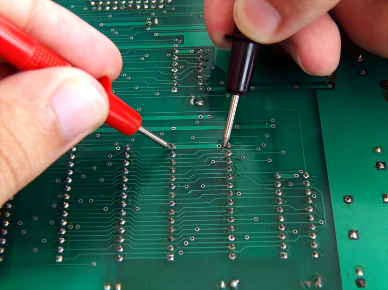
Stencil printing is a powerful method for duplicating designs, but it has its drawbacks. One of the main challenges is the limited accuracy when compared to modern laser cut stencils. Traditional stencil printing often requires manually adjusting the design or material, which can lead to human error. In contrast, laser cut stencils ensure consistency, with precision tolerances as tight as ±4 μm, ensuring that every cut is perfect.
Another issue is the wear and tear of reusable stencils. Over time, traditional stencils may degrade, leading to blurred edges or design distortions. With laser cut stencils, this issue is minimized, as the laser cutting process results in clean, sharp edges that last longer.
What Is the Best Material for Laser Cut Stencils?
The material you choose for a laser cut stencil plays a significant role in its performance and durability. For most projects, mylar stencil sheets are a popular choice due to their flexibility, ease of use, and durability. Mylar is a strong material that holds up well against repeated use, especially in laser cut stencils for screen printing.
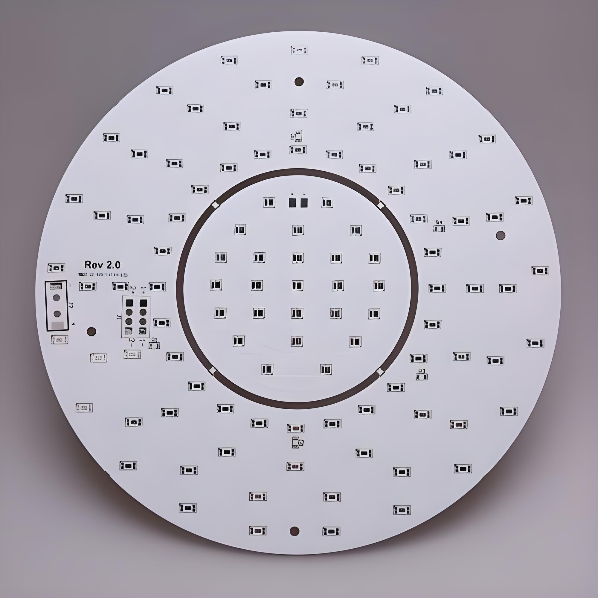
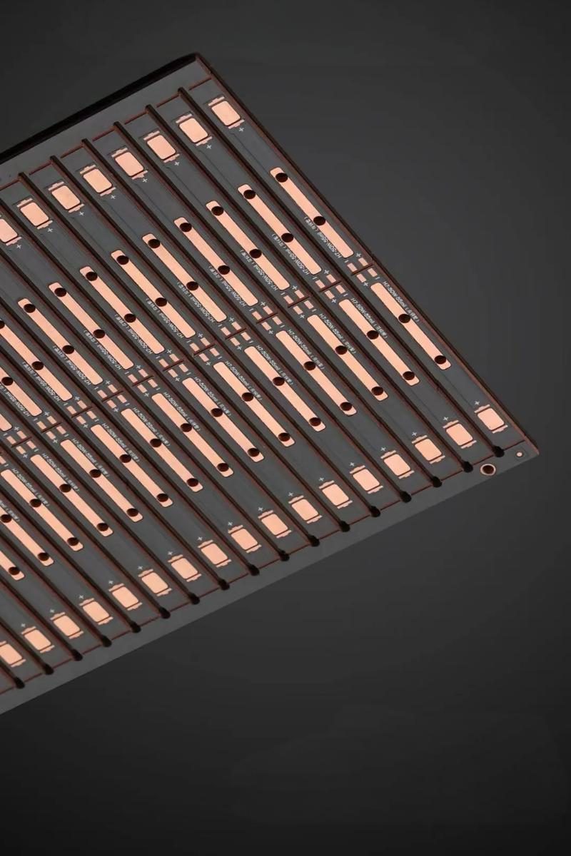
Stainless steel is another excellent material for laser cut stencils, especially for industrial applications like SMT stencils. This material offers unmatched durability and strength, and it’s often electro-polished for a smooth finish. Stainless steel laser cut stencils are also highly resistant to corrosion, making them ideal for repeated use in harsh environments.
The best material will depend on the specific application, but both mylar stencils and stainless steel are reliable options that deliver high-quality results.
What Is the Best App to Make Stencils?
Making a laser cut stencil requires precision, and that starts with the design. The best apps for creating stencils offer flexibility and control over intricate details. Popular software tools like Adobe Illustrator, CorelDRAW, and Inkscape allow you to create detailed vector designs that are perfect for laser cutting.
For PCB manufacturers, software that directly imports Gerber files, such as AutoCAD or Eagle, can be incredibly helpful. EBest Circuit (Best Technology)’s stencils, for example, are made with precision from customer-provided files, which minimizes the chances of errors and ensures that every detail is captured accurately.
The right app will depend on your project’s needs, but these tools are essential for creating custom laser cut stencils that are both precise and professional.
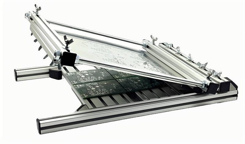
How Are Professional Stencils Made?
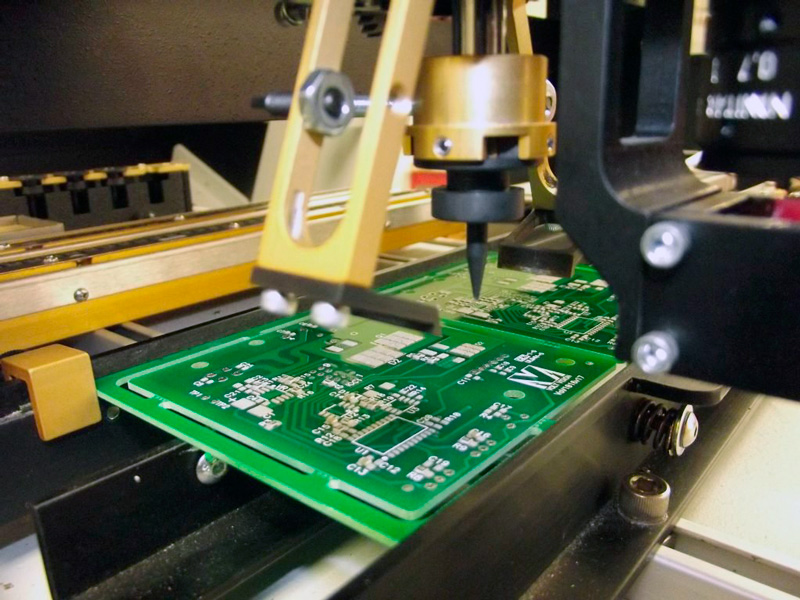
Professional laser cut stencils are made with precision equipment and high-quality materials. The process typically starts with a detailed design, often created in vector format. This design is then uploaded to a laser cutting machine, which uses a focused laser beam to cut the design into the material, whether it’s mylar, stainless steel, or another substrate.
At EBest Circuit (Best Technology), for example, we offer SMT stencils made from stainless steel with tolerances as tight as ±4 μm. These stencils are laser cut for ultimate precision and are often electro-polished to ensure smoothness. The end result is a stencil with clean edges and consistent openings that help reduce solder paste printing errors.
How Can Custom Laser Cut Stencils Improve Your Screen Printing Projects?
Custom laser cut stencils are a game-changer for screen printing. They offer precision that traditional stencils cannot match, ensuring that designs are transferred accurately every time. The ability to customize the size, shape, and number of openings allows for greater flexibility in design.
For example, laser cut stencils for screen printing ensure smoother paste release and cleaner edges. This reduces the need for frequent stencil cleaning, which can improve the overall efficiency of the printing process. Custom stencils are particularly valuable for complex designs, such as laser cut stencils for painting or laser cut stencils for industrial use, where accuracy is critical.
Moreover, custom laser cut stencils help streamline production times. Since they are made with high precision, the risk of errors is reduced, leading to fewer reprints and more consistent results in the long term.
What Is the Difference Between Laser Cut Stencils and Traditional Stencils?
The main difference between laser cut stencils and traditional stencils lies in the precision and versatility of the cutting process. Laser cut stencils are made using advanced technology that offers tighter tolerances, sharper edges, and more consistent results than traditional hand-cut stencils. Additionally, the laser cutting process allows for greater customization in terms of size, shape, and material choice.
Traditional stencils, while effective for simpler tasks, often require more labor-intensive processes and can lead to more inaccuracies, especially when dealing with intricate designs. In contrast, laser cut stencils are designed with a high level of detail and precision, ensuring that even the most complex patterns are reproduced flawlessly.
In a nutshell, whether you’re working on screen printing, PCB manufacturing, or an artistic project, a lasercut stencil is an invaluable tool that offers precision, durability, and customization. Laser cutting technology has revolutionized stencil making, allowing for the production of high-quality, accurate stencils that meet a wide range of needs.
At EBest Circuit (Best Technology), we pride ourselves on providing laser cut stencils for SMT applications with state-of-the-art technology and attention to detail. Our high-quality laser cut stencils are made from durable materials like stainless steel and are electro-polished for a smooth finish. With fast delivery and customizable options, EBest Circuit (Best Technology) is your trusted partner for all your stencil needs. Feel free to contact us at sales@bestpcbs.com for any doubts or queries you might have.