What makes copper plated PCB the top choice for high‑reliability electronics in medical, aerospace, and industrial applications? This guide fully explains copper plated PCB design, prototyping, assembly, quality control, and industry applications, and shows why EBest is your best partner for all copper plated PCB solutions.
Why Choose EBest as Your Copper Plated PCB Manufacturer?
Here are reasons why choose EBest as your copper plated PCB manufacturer:
- One-Stop Service: We handle the full production flow of copper plated PCB, from design and prototyping to mass production and assembly. Working with a single partner simplifies your workflow, cuts down coordination work, and keeps quality stable across production.
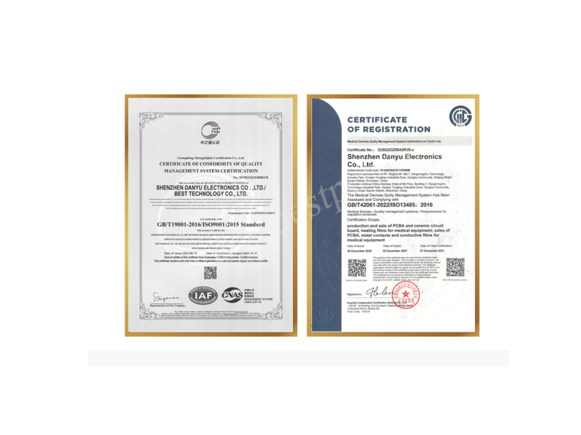
- Certified Quality Standards: EBest holds IATF 16949, ISO 9001, ISO 13485, AS9100D, RoHS, REACH, and UL certifications. These qualifications ensure copper plated PCB fully meets strict requirements for medical, aerospace, automotive, and industrial equipment.
- Advanced Manufacturing Technology: Our precision plating process delivers uniform coating, strong adhesion, and long-term stability for copper plated PCB. We effectively avoid common defects and support high-aspect-ratio vias, thick copper layouts, and high-frequency designs.
- Strong Capacity & Fast Delivery: With large-scale production capacity and support for diversified board designs, we handle both prototype and mass orders smoothly. Expedited services are available for urgent copper plated PCB projects to keep your project on schedule.
- Professional Engineering Support: Our engineering team provides free DFM analysis and targeted optimization for your copper plated PCB. This helps improve production yield, product reliability, and overall performance.
- Proven Industry Experience: We have rich experience serving medical devices, aerospace systems, and industrial equipment. Our copper plated PCB performs reliably in demanding environments and critical applications.
Copper Plated PCB Design: Common Pain Points & Our Solutions
Common Pain Points in Copper Plated PCB Design
- Uneven copper thickness leading to inconsistent conductivity.
- High aspect ratio holes with insufficient plating coverage.
- EMI and crosstalk in high-frequency layouts.
- Thermal stress causing trace or via cracking.
- Design rules unaligned with production capabilities.
How EBest Solves Copper Plated PCB Design Challenges
- DFM review and layer stack optimization for balanced copper distribution.
- Controlled impedance and grounding strategies to reduce EMI.
- Thermal relief and high‑TG material recommendations.
- Precise trace and via sizing per IPC standards.
- 24/7 engineering support for design adjustments.
Trust EBest for professional copper plated PCB design that ensures performance, yield, and long‑term reliability.
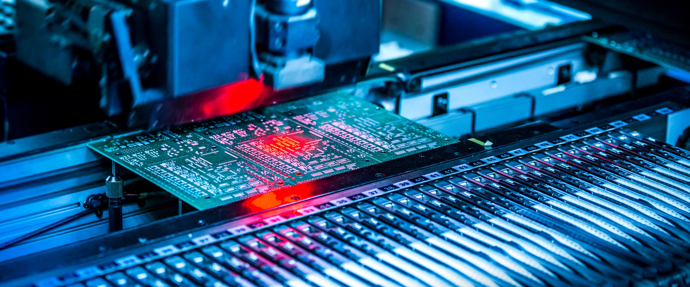
Copper Plated PCB Prototype: Challenges & Fast Solutions
Common Prototype Problems
- Unstable copper thickness across traces and vias.
- Weak bonding or voids in plated through holes.
- Board deformation caused by uneven stress.
- Long turnaround time blocking rapid verification.
EBest Prototype Solutions
- Precision plating lines with real‑time thickness monitoring.
- Strict surface pretreatment to improve bonding strength.
- Symmetrical layer design to reduce warpage risk.
- Quick‑turn prototyping with fast delivery for urgent projects.
For high‑quality, on‑time copper plated PCB prototypes, EBest is your trusted partner.
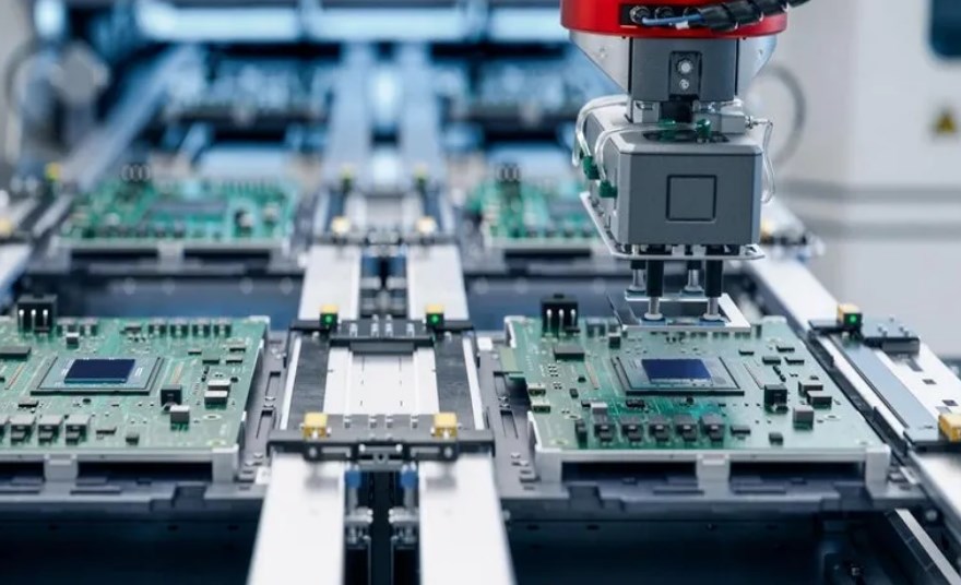
Copper Plated PCB Assembly: Reliability & Yield Improvements
How does copper plated PCB quality affect assembly yield? Poor plating leads to weak solder joints, component shifting, tombstoning, bridging, and thermal damage, all of which reduce production efficiency and field reliability.
Typical Copper Plated PCB Assembly Pain Points
- Poor solderability caused by oxidation or uneven surface.
- Tombstoning and misalignment due to unbalanced heating.
- Solder bridging in high‑density thick copper layouts.
- Thermal stress damaging copper layers during reflow.
Our Assembly Optimization Solutions
- Stable surface finishes ensuring consistent soldering.
- Optimized stencil design and printing parameters.
- Reflow thermal profiling customized for copper thickness.
- Full inspection including AOI, X‑ray, and functional testing.
For high‑yield, high‑reliability copper plated PCB assembly, choose EBest.
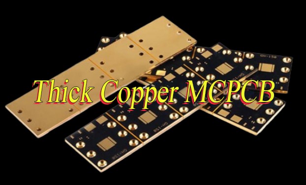
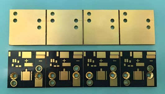
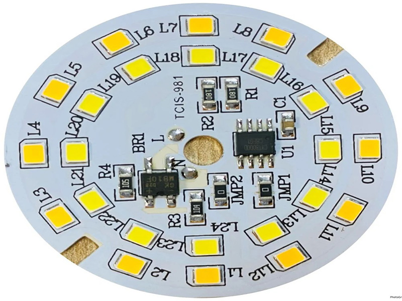
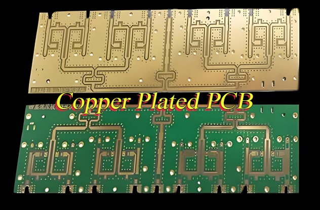
What Is Copper Plated PCB & How Does It Work?
A copper plated PCB is a printed circuit board with a reinforced copper layer applied to its surface and inside all plated through holes and vias. This plating improves electrical conductivity, current carrying capacity, heat dissipation, and structural stability, making it essential for high‑reliability electronics.
Copper plating creates continuous conductive paths between layers, lowers resistance, reduces signal loss, and strengthens vias against cracking or failure. It is widely used in medical, aerospace, industrial, and high‑power applications where stable performance under stress is critical.
At EBest, our copper plated PCB uses precision plating to ensure uniform thickness, strong adhesion, and long‑term durability for mission‑critical devices.

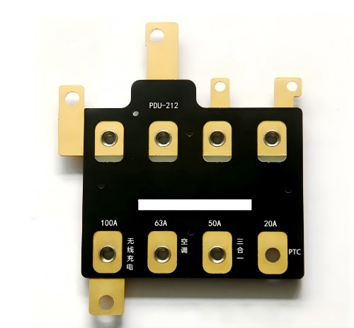
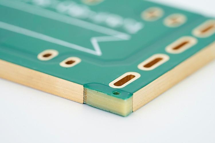
How Thick Should Copper Plating Be on a PCB?
Copper plating thickness directly determines current capacity, thermal performance, and reliability of a copper plated PCB. The right thickness prevents overheating, voltage drop, and premature board failure.
Standard thickness ranges include 0.5–1 oz for low‑power consumer electronics, 1–3 oz for industrial and automotive use, and 3–10 oz for high‑power, aerospace, and heavy‑duty equipment.
EBest engineers help you select the optimal copper thickness based on your current load, working environment, and industry standards to balance performance and reliability.
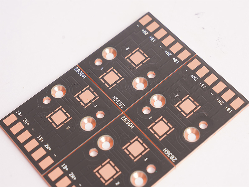
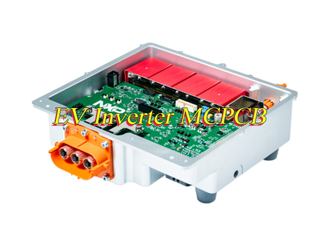
How to Improve Copper Plated PCBs Reliability in Medical & Aerospace?
Medical and aerospace electronics require zero-failure performance under extreme temperatures, vibration, and long-term operation. Copper plated PCB reliability must be engineered at the material, process, and design levels to meet these strict demands.
- Use high-TG and low-CTE base materials to minimize thermal expansion and avoid layer separation or via cracking in repeated temperature cycles.
- Maintain strict copper plating thickness to meet IPC Class 3 standards, ensuring full, uniform coverage in high aspect ratio vias with no voids or weak points.
- Adopt thermal relief structures and reinforced via/pad designs to reduce stress concentration and improve resistance to shock and vibration.
- Apply enhanced surface treatment and bonding processes to maintain stable conductivity and prevent oxidation, peeling, or delamination.
- Perform full reliability validation including thermal shock, temperature cycling, humidity testing, and mechanical vibration to ensure long-term stability.
- Follow ISO 13485 for medical devices and AS9100D for aerospace systems to ensure full traceability, consistency, and compliance.
- Optimize layer stack and copper distribution to balance internal stress and avoid board warping or deformation in critical applications.
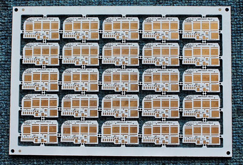
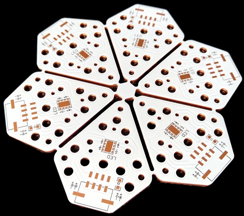
What Are Common Defects in Copper Plated PCB Manufacturing?
Copper plated PCB defects directly affect conductivity, reliability, and assembly yield. Most issues come from uneven plating, insufficient pretreatment, poor process control, or unbalanced design.
- Uneven copper plating thickness across traces, pads, and vias, leading to inconsistent conductivity and localized overheating.
- Voids or incomplete plating inside through holes and vias, causing open circuits or weak, unstable electrical connections.
- Poor adhesion between copper plating and the base material, resulting in blistering, peeling, or delamination during use.
- Rough or nodular copper surface that reduces solderability and increases the risk of assembly defects.
- Board warpage or twisting caused by unbalanced copper layout, asymmetric lamination, or uneven plating stress.
- Burning or discoloration in dense or thin circuit areas due to improper current control during plating.
- Insufficient coverage on high-aspect-ratio vias, which reduces structural strength and leads to early field failure.
How Does Copper Plated PCBs Enhance Thermal Management?
Effective thermal control is critical for high-power and high-reliability electronics. Copper plated PCB greatly improves heat dissipation using the high thermal conductivity of copper.
- Copper transfers heat rapidly from heat-generating components to the entire board surface, reducing localized overheating.
- Thick, uniform copper layers spread heat evenly, eliminate hotspots, and lower the operating temperature of key components.
- Plated vias and copper planes create efficient heat paths to heat sinks, chassis, or external cooling systems.
- Higher copper thickness reduces thermal resistance between layers, boosting overall cooling efficiency in high-power devices.
- Better thermal management reduces thermal fatigue, extending service life in industrial, medical, and aerospace environments.
- Balanced copper distribution reduces thermal stress, protecting against trace cracking, board warping, and premature failure.
FAQs About Copper Plated PCB Board
Q1: What is the main difference between copper plated PCB and standard PCB?
A1: Copper plated PCB has reinforced plating layers for better conductivity, higher current capacity, improved heat dissipation, and stronger structural reliability.
Q2: Which industries use copper plated PCB most widely?
A2: Medical devices, aerospace systems, industrial equipment, automotive electronics, power supplies, and high‑frequency communication devices.
Q3: What copper thickness is suitable for high‑current applications?
A3: 3 oz to 10 oz or heavier copper plating is typically recommended for high‑current designs.
Q4: Can you produce copper plated PCB for medical equipment?
A4: Yes, we are ISO 13485 certified and support Class I to Class III medical devices.
Q5: Do you support aerospace‑grade copper plated PCB?
A5: Yes, we hold AS9100D and provide high‑reliability boards for aerospace and aviation systems.
Q6: How fast can you deliver copper plated PCB prototypes?
A6: We offer expedited services with delivery within 24 hours for urgent orders.
Q7: What quality standards do you follow for copper plated PCB?
A7: We follow IPC‑A‑600, IPC‑6012, plus IATF 16949, ISO 9001, ISO 13485, AS9100D, RoHS, REACH, and UL requirements.
Q8: Can you manufacture heavy copper plated PCB?
A8: Yes, we support thick copper, heavy copper, and high‑power circuit designs.
Order Copper Plated PCB From EBest Today
EBest provides full‑service solutions for copper plated PCB and copper plated PCB board, covering design, prototyping, mass production, and assembly. If you need high‑quality, reliable, and fast‑delivery copper plated PCB, please contact us via email: sales@bestpcbs.com to place your order.