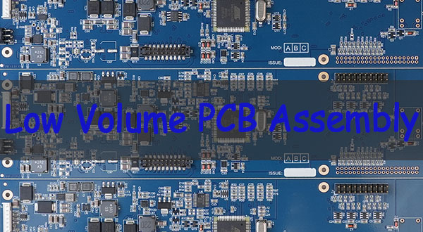
Looking for PCB manufacturer in Zimbabwe? This guide covers top 10 manufacturers, pain points, selection criteria, capacity evaluation, lead time analysis, 2026 challenges, and FAQs to help you navigate Zimbabwe’s PCB market confidently.
When looking for reliable PCB manufacturing solutions in Zimbabwe, understanding the local market landscape and identifying reputable providers is crucial. The top 10 PCB manufacturer in Zimbabwe represent the core strength of the regional PCB industry, offering a range of services tailored to different project requirements. Whether it’s prototype development or mass production, these top 10 PCB manufacturer in Zimbabwe cover various technical specifications and delivery needs, making them the primary choice for businesses seeking PCB manufacturer in Zimbabwe.

Top 10 PCB Manufacturer in Zimbabwe
| Company Name | Core Business | Process Capability | Lead Time |
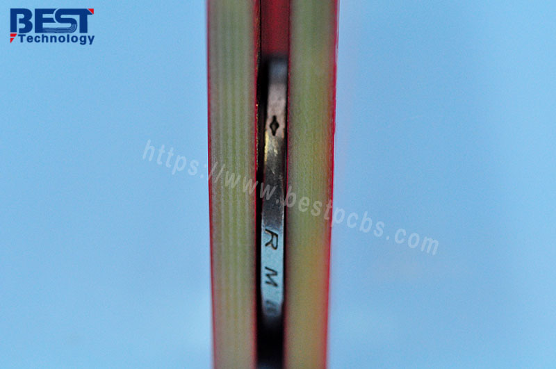
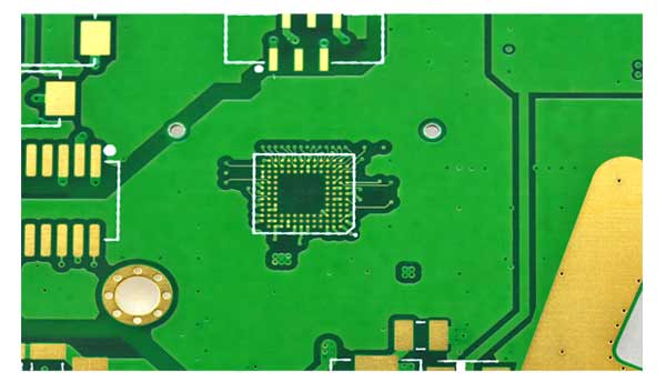
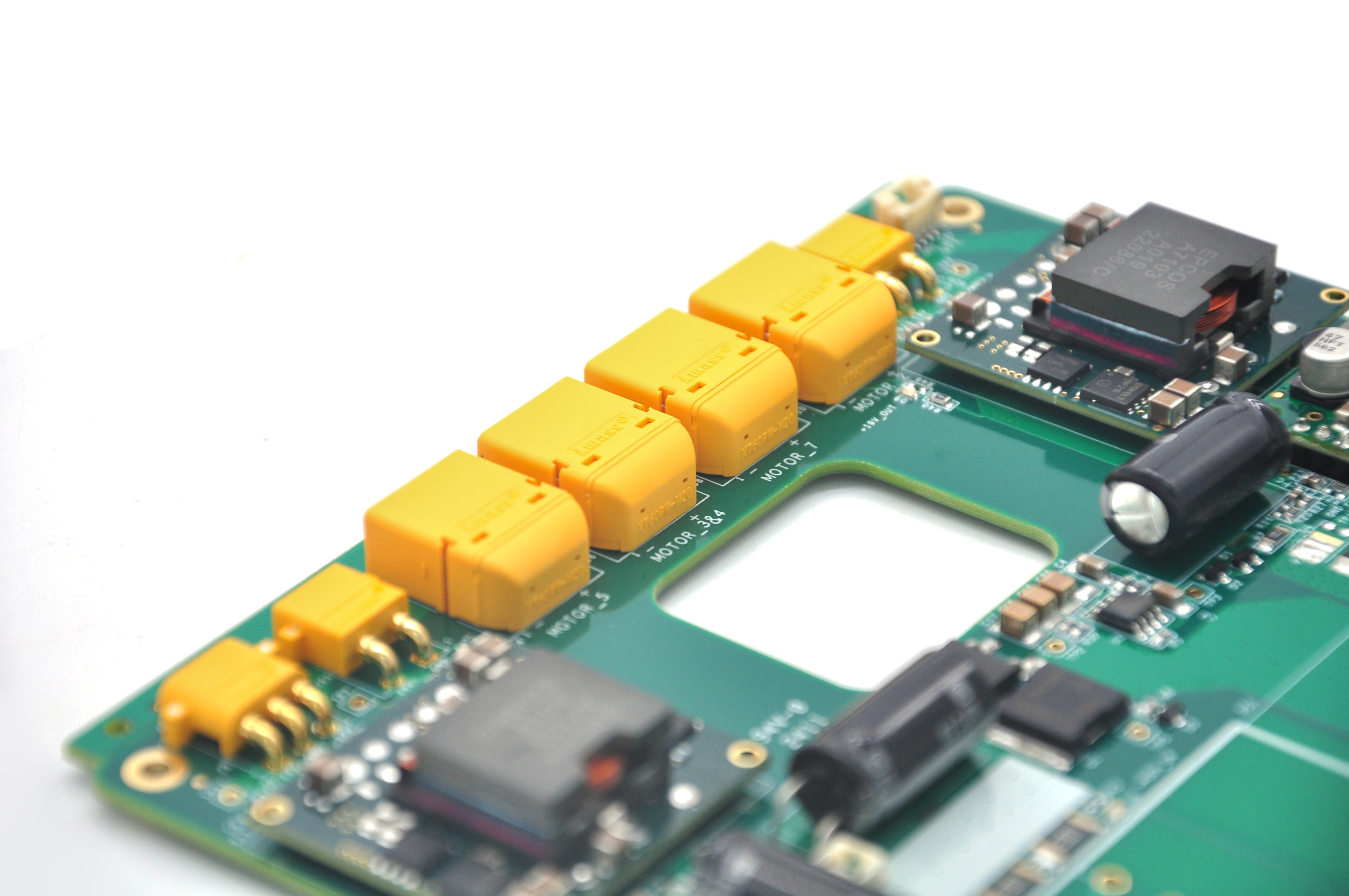
| EBest Circuit (Best Technology) Co.,Ltd. | Multilayer PCB fabrication, PCB assembly, prototype development | Supports 1-24 layer PCBs; line width/spacing 3/3 mil; LDI exposure (±1.5μm accuracy); RoHS/UL compliant | Prototypes: 3-5 days; Mass production: 7-12 days |
| KAISHENG PCB Zimbabwe | Turnkey PCB assembly, SMT & Thru-hole mixed assembly, PCB fabrication | 1-8 layer PCBs; order volume 1-500,000 pcs; AOI & X-Ray testing; DFM analysis | Prototypes: 3 days; Mass production: 3-4 weeks (free shipping for bulk orders) |
| Trend Systems (Pvt) Ltd | Industrial control PCB manufacturing, custom PCB fabrication, component sourcing | 1-12 layer PCBs; FR-4 substrate; copper thickness 1oz-3oz; solder mask: green/black | Prototypes: 5-7 days; Mass production: 10-15 days |
| Arachnid Design Zimbabwe | High-frequency PCB fabrication, PCB design support, small-batch production | 1-6 layer PCBs; line width/spacing 4/4 mil; Rogers substrate available; impedance control | Prototypes: 4-6 days; Mass production: 8-12 days |
| Tech24 Group | Consumer electronics PCB manufacturing, PCB assembly, testing services | 1-10 layer PCBs; SMT assembly (0402 component size); yield rate ≥98% | Prototypes: 3-5 days; Mass production: 7-10 days |
| Net Byte Technologies Pvt Ltd | Communication PCB fabrication, prototype sampling, medium-batch production | 1-8 layer PCBs; FR-4 & aluminum-based substrates; interlayer alignment tolerance ≤25μm | Prototypes: 5-8 days; Mass production: 12-16 days |
| Craft Solutions Zimbabwe | Medical equipment PCB manufacturing, high-reliability PCB assembly | 1-16 layer PCBs; IPC Class 6012B compliant; lead-free soldering; temperature resistance TG 180°C | Prototypes: 6-8 days; Mass production: 14-20 days |
| Novea Tech Zimbabwe | Automotive PCB fabrication, custom prototype development, PCB testing | 1-12 layer PCBs; line width/spacing 3/3 mil; vacuum etching; AOI testing | Prototypes: 4-6 days; Mass production: 9-13 days |
| Scan Top IT Solutions | Digital device PCB manufacturing, small-batch PCB assembly, DFM consultation | 1-6 layer PCBs; FR-4 substrate; copper thickness 1oz-2oz; solder mask customization | Prototypes: 5-7 days; Mass production: 10-14 days |
| Micro Man Zimbabwe | Legacy electronic PCB manufacturing, replacement PCB fabrication, low-volume production | 1-4 layer PCBs; traditional thru-hole assembly; compatibility with old electronic systems | Prototypes: 7-10 days; Mass production: 15-20 days |
Pain Points of PCB Manufacturer in Zimbabwe
- The lack of localized DFM (Design for Manufacturability) support leads to a 15-20% increase in design modification rates for PCB projects in Zimbabwe.
- Given that only 35% of local manufacturers have 24-hour rapid prototyping capabilities, the prolonged prototype lead time (average 5-8 days) hinders project progress.
- Due to the high cost of imported high-end materials (accounting for 40-50% of production costs), PCB manufacturers in Zimbabwe struggle to meet the demand for high-temperature and high-frequency substrates.
- With the defect rate of small-batch production averaging 0.8-1.2% locally, the insufficient precision of etching equipment (vacuum etching lines coverage rate <60%) is the main contributing factor.
- The unstable supply of key raw materials (such as copper clad laminates) due to import tariff fluctuations leads to production delays of 3-7 days for 60% of manufacturers.
- The lack of professional technical personnel in high-layer PCB manufacturing (16+ layers) restricts the ability of local PCB manufacturers in Zimbabwe to undertake complex projects.
- Due to the low penetration rate of advanced testing equipment (X-Ray testing available in only 40% of manufacturers), PCB products face higher quality risks in terms of internal soldering defects.
How to Choose A Reliable PCB Manufacturer in Zimbabwe?
Selection Guide to PCB Manufacturer in Zimbabwe:
- Prioritize manufacturers with IPC Class 6012B, UL and RoHS certifications. These certifications cut non-conforming product risks by 70% compared to uncertified ones.
- Match process capability to your project needs. For high-precision projects, choose manufacturers with LDI exposure (±1.5μm accuracy) and line width/spacing ≤3/3 mil, this ensures over 98% pass rate for complex circuits.
- Check raw material supply stability. Ask for supply chain records; manufacturers with long-term partnerships with global suppliers (e.g., Rogers, FR-4) have 35% fewer material shortage delays.
- Compare lead times against local benchmarks. Optimize for 3-5 day prototype lead times (Zimbabwe’s optimal standard); avoid manufacturers with lead times over 8 days, as this can extend project cycles by 20-30%.
- Assess after-sales support. Choose manufacturers offering 72-hour technical responses, timely resolution of post-delivery issues can reduce rework costs by up to 45%.
- Review historical performance. Prioritize manufacturers with ≥98% mass production yield and <0.5% defect rate for high-volume orders (1000+ units), which meets global advanced standards.
How to Evaluate Production Capacity of PCB Manufacturer in Zimbabwe?
Evaluation Guide to Production Capacity of PCB Manufacturer in Zimbabwe:
- Inspect production facility scale, including workshop area and equipment configuration; manufacturers with a production area of ≥5000 m² and automated production lines (e.g., automatic lamination machines) have stronger large-batch production capacity.
- Verify monthly production capacity data, such as monthly output of square meters of PCBs and component assembly volume; a monthly capacity of ≥10,000 square meters indicates the ability to undertake medium to large projects.
- Evaluate technical team strength, including the proportion of technical personnel (preferably ≥35%) and their years of industry experience; teams with more than 10 years of experience have a 50% higher efficiency in solving production technical problems.
- Test sample production capability by requesting a prototype of the target product; assess whether the sample meets design specifications, including circuit accuracy, solder mask uniformity, and hole position precision.
- Review certification and compliance credentials, such as IPC, UL, RoHS, and ISO certifications; the number of authoritative certifications reflects the manufacturer’s standardized production level and quality control capabilities.
- Investigate the ability to handle special processes, such as high-frequency PCB fabrication, impedance control, and lead-free soldering; this determines whether the manufacturer can meet customized project requirements.
- Analyze historical order completion data, including on-time delivery rate for large-batch orders (preferably ≥95%) and customer feedback on product stability; this reflects the manufacturer’s actual production reliability.

How to Evaluate Lead Time of PCB Manufacturer in Zimbabwe?
Evaluation Guide to Lead Time of PCB Manufacturer in Zimbabwe:
- Request a detailed lead time breakdown, including material procurement time, production process time, testing time, and shipping time; a transparent breakdown indicates effective production schedule management.
- Verify the manufacturer’s historical on-time delivery rate; prioritize those with an on-time delivery rate of ≥95% for orders of the same type and volume as the target project.
- Evaluate the flexibility of production scheduling, such as whether expedited services are available for urgent orders and the additional cost ratio (preferably ≤20% of the total order value) for expediting.
- Investigate the stability of the supply chain for key raw materials; manufacturers with safety stock of core materials (≥15 days of production demand) have lower risk of material shortage delays.
- Assess the efficiency of the testing process, including the number of testing equipment and testing personnel; manufacturers with automated testing equipment (e.g., AOI, X-Ray) can reduce testing time by 30-40%.
- Confirm the clarity of delivery commitment clauses in the contract, including penalty provisions for delayed delivery; formal penalty terms (e.g., 1-2% of the order value per day of delay) ensure the manufacturer’s responsibility for lead time.
- Collect customer feedback on lead time reliability, such as whether there have been frequent unforeseen delays and the manufacturer’s response measures for delays; this reflects the actual lead time performance in practice.
Challenges Faced by the PCB Industry in Zimbabwe in 2026
- Sustained inflation and rising labor costs could increase overall production costs by 15-20%, squeezing profit margins for Zimbabwean PCB manufacturers.
- The proposed VAT increase in Zimbabwe’s 2026 national budget may suppress market demand for electronic products, leading to reduced order volumes for local PCB manufacturers.
- Inadequate rural infrastructure, particularly unreliable power supply and poor internet connectivity, may limit PCB manufacturers’ capacity expansion and remote technical support capabilities.
- Global supply chain fluctuations driven by the inventory build-up for Nvidia’s Rubin platform in 2026 could lead to shortages and price increases of key electronic components, affecting the production stability of PCB manufacturers.
- Stringent global environmental regulations (e.g., EU RoHS and WEEE directives) require local manufacturers to switch to environmentally friendly materials and processes, increasing initial investment costs by 25-30%.
- Limited access to credit for small and medium-sized PCB manufacturers may hinder technological upgrades and equipment modernization, impacting their competitiveness in the global market.
- Low PCB e-waste recycling rates (only 20-30% globally) may lead to stricter regulatory scrutiny, requiring manufacturers to invest in additional waste treatment facilities.
- A shortage of skilled personnel in advanced PCB manufacturing areas (e.g., HDI boards, IC substrates) may limit the industry’s ability to upgrade to high-end product markets.
FAQ about PCB Manufacturing in Zimbabwe
Q1: What should I pay attention to when designing PCBs for manufacturing by PCB Manufacturer in Zimbabwe?
A1: Prioritize DFM compliance; avoid line width/spacing ≤3/3 mil if not necessary (only 60% of local manufacturers support this precision). Confirm substrate availability (FR-4 is widely available, while high-frequency substrates need advance booking) and provide clear impedance control requirements if applicable.
Q2: How to ensure the quality of PCB prototypes from manufacturers in Zimbabwe?
A2: Request pre-production sample testing reports (AOI or X-Ray). Choose manufacturers with a prototype defect rate <0.8% and confirm that they offer rework services for non-conforming prototypes within the lead time without additional costs.
Q3: What is the average lead time for mass production of PCBs in Zimbabwe, and how to shorten it?
A3: Average lead time is 7-15 days. To shorten it, place orders during the manufacturer’s off-peak season, provide complete design files in advance, and choose manufacturers with safety stock of raw materials and automated production lines.
Q4: Are PCB manufacturers in Zimbabwe capable of producing high-temperature resistant PCBs for automotive use?
A4: Yes, but select manufacturers compliant with IPC Class 6012B and using TG 180°C-220°C substrates. Verify their automotive PCB production experience (e.g., historical order cases) and temperature resistance test reports.
Q5: How to resolve disputes with PCB Manufacturer in Zimbabwe regarding product quality or delivery delays?
A5: Sign a formal contract with clear quality standards and delivery penalty clauses in advance. Preserve all communication records and test reports. Seek third-party industry testing institutions for verification if there are quality disputes, and enforce penalty provisions for delays as per the contract.