What are USB Ports?
The USB end is a connection for connecting a consumer electronics device such as an accounting machine. USB’s general name is a universal skewer line. USB end support USB support for connection. If you have a USB connection, you can set up a number of numbers. In addition, a USB port is also available, as well as a power supply. This end is fully equipped with the power.
The USB calculation function has additional functions, and one small adjustment can be made alternately. Please contact us if you have any questions about USB. With the advancement of technology, the current functionality of the USB end is greatly enhanced. Because of this, this is a small change to the end of the road. USB is important for three major directions. In this regard, the dimensions are the external size, the number of speeds, the visual power of the power.
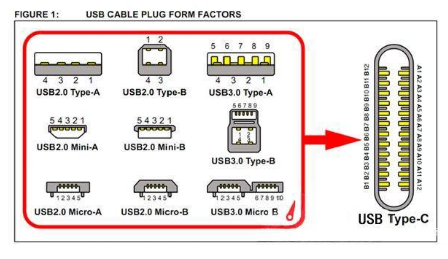
Usb connector types
Types of USB connectors: different types of connectors with different shapes and directions, USB connectors can be separated into different types:
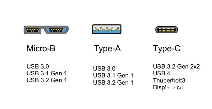
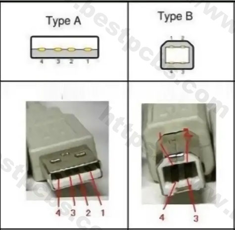
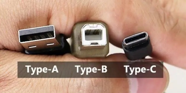
Type-A port: This is the most common type of USB port, the shape is long and rectangular, and the support is heat-resistant. Computer equipment such as printing machine, keypad, mouse button, driving device, etc. Type-A interface has USB 2.0 and USB 3.0 in different editions, among which USB 3.0 has faster speed, color is usually blue, and USB 2.0 has slow speed, color is black.
Type-B contact: Type-B contact shape is round shape, demand-specific connection. For general use, external equipment such as audio equipment, viewing equipment, etc., such as a 3.5 inch movable screen, stamping machine, display device, etc.Type-B verbal usage scene is relatively small, so this is an unusual sight in daily life.
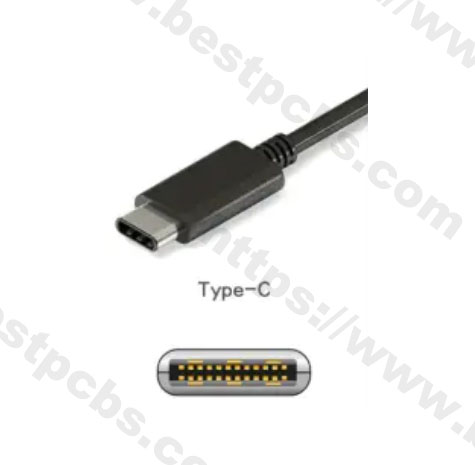
Type-C port: Type-C port is a new type of USB port that has emerged in recent years. Built-in USB 3.1, Type-C interface configuration, mainstream interface type, intelligent handheld computer, flat panel battery, notebook battery, etc. The biggest feature of the Type-C interface is its support and double-sided insertion, making it convenient and convenient to use.
Type-C interface support further improves the speed and power of the power, and provides more advanced usage experience. Previously, when I came here, I was confused as to how to get around the main machine.
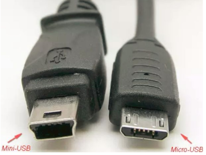
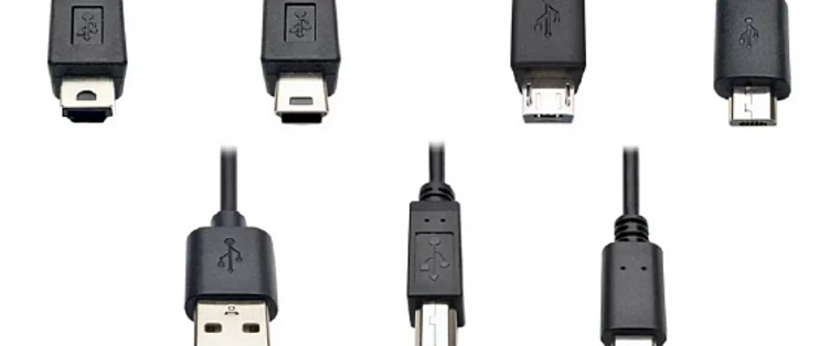
Mini USB port Micro USB port
Mini USB port Micro USB port: There are many types of ports for transfer equipment, digital reading machine, digital image machine, metering equipment, etc. Mini USB port ratio Micro USB port size is small, also known as a USB port, Micro USB port is smaller, thinner, supports OTG function, and provides a number of additional power functions. The Micro USB port is convenient and easy to use, and has various types of portability.
What functions does USB have?
- Power Delivery of USB Ports
Some USB cables can deliver power as well as transfer data, but most USB cables can do both. Power delivery of USB ports is mainly divided into three categories: fast charging, quick charging, and power only. - USB Data Transfer Speed
USBs come in various sizes and shapes. Also, USB types have multiple speed standards. It is important to know that some USB cables are designed for data transfer only, while some can only deliver power. However, some USB cables can serve both purposes at the same time. Therefore, it is necessary to verify the performance of the cable before purchasing it. - USB Video Transfer
The ability of USB ports to power devices and transfer data between devices is already impressive enough. However, you can decide to integrate USB-C to connect a monitor in place of a VGA cable or HDMI. In addition, USB-C also supports 4K video transmission.
What are the advantages of USB interface?
- Standard uniformity. The most common ones are hard disks with IDE interfaces, mouse and keyboards with serial ports, and printers and scanners with parallel ports. However, with USB, all these application peripherals can be connected to personal computers using the same standard. At this time, there are USB hard disks, USB mice, USB printers, etc.
- Easy to carry. Most USB devices are known for being “small, light, and thin”, which is very convenient for users to carry large amounts of data with them.
- Hot-swappable. That is, when users use external devices, they do not need to shut down and restart the computer, but directly plug in the USB when the computer is working.
- Multiple devices can be connected. USB often has multiple interfaces on personal computers, and several devices can be connected at the same time. If a USB HUB with four ports is connected, four USB devices can be connected, and so on. You can connect all the devices to a personal computer at the same time without any problems (up to 127 devices can be connected).
How Do USB Ports Work?
USB is an external bus standard used to regulate the connection and communication between computers and external devices. The USB interface has plug-and-play and hot-swap functions. The USB interface can connect 127 peripherals, such as mice and keyboards. USB was jointly launched by Intel and other companies in 1994 and has successfully replaced serial and parallel ports since 1996. It has become a must-have interface for computers and a large number of smart devices today. For most engineers, the main obstacles to developing USB2.0 interface products are: facing the complex USB2.0 protocol, writing USB device drivers by themselves, and being familiar with microcontroller programming.
Why USB Ports Are Replacing Serial Ports
USB has three major advantages. It is superior to serial ports in several aspects.
Speed
USB ports are able to transfer data at a much faster speed. They work ten times faster than regular parallel ports. Also, they are much faster than serial ports. On average, serial ports offer a data transfer rate of 150kbps. On the other hand, USB ports offer about 12 Mbps. The data transfer rate depends on the type of USB port. For example, USB 2.0 has a maximum data transfer rate of 480 Mbps.
Compatibility
USB ports have replaced serial ports in the past few years. Various industrial devices are equipped with serial ports. This replacement has brought problems. USB ports are generally compatible with most USB devices.
Durability
USB ports are more durable than serial ports. The tiny pins on a serial port can break or bend easily. Whereas USB ports are very sturdy.
Frequently Asked Questions
The USB interface cannot be used. It may be due to a problem with the system. You need to check whether the system service is disabled or reinstall the operating system.
BIOS setting problem. If USB is disabled in BIOS or CMOS, you need to restore it to the factory default settings.
USB driver is not installed or the driver is deleted. You need to install the USB universal driver.
The front USB cable is not connected properly. Try to insert the USB flash drive into the USB interface on the back of the chassis.
The USB interface voltage is insufficient. When the mobile hard disk is connected to the front USB interface, it may not be recognized due to insufficient voltage. You should use a hard disk box with an external power supply or replace the power supply.
Compatibility issues between the motherboard and the system. For example, the compatibility issues between the NF2 motherboard and USB require the installation of the latest dedicated USB2.0 driver and patch.
System or BIOS problem. When USB is disabled in the BIOS or operating system, you need to enable options related to USB devices.
Be careful when plugging and unplugging. Do not unplug during reading and writing, otherwise the chip may be burned.
If the USB device is frequently disconnected, it may be that the USB cable connection is unstable or there is a problem with the USB port. Try changing the cable or connecting to another USB port.
If the USB device cannot be recognized or charged, make sure the device is compatible and the cable is intact. Try connecting to another computer or updating the driver.