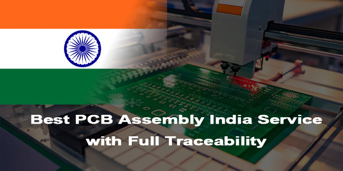
EMI shield PCB architecture is now a critical design element in high-speed, high-frequency electronic systems. As operating frequencies increase and circuit density continues to rise, electromagnetic interference directly impacts signal integrity, RF stability, and EMC compliance margins. This article explores how EMI shield PCB structures work, how PCB EMI shield solutions are implemented in manufacturing, and what engineers should consider to ensure reliable, compliant performance.
At EBest Circuit (Best Technology), we support EMI-sensitive designs with fully integrated in-house capabilities covering PCB fabrication, component sourcing, SMT assembly, testing, and box-build integration. With over 20 years of manufacturing experience, we have served more than 1,800 customers across industrial, automotive, medical, and aerospace sectors. Our engineering team provides free DFM analysis and process adaptation suggestions to optimize shielding effectiveness before production begins. We operate under ISO9001, ISO13485, IATF16949, and AS9100D quality systems. Whether you require rapid prototyping or volume production, pls feel free to contact us via sales@bestpcbs.com.
What Is an EMI Shield PCB and Why Is It Critical in Modern Electronics?
An EMI shield PCB is a printed circuit board designed with structural or physical shielding measures to suppress electromagnetic interference. The shielding may be achieved through multilayer stack-up optimization, grounded shielding cans, via fencing, conductive coatings, or a combination of these techniques.
Modern electronics operate at increasingly higher frequencies. Fast edge rates, switching regulators, dense layouts, and wireless modules generate unintended electromagnetic radiation. Without proper control, this radiation can:
Distort high-speed signals
Trigger instability in analog circuits
Interfere with wireless modules
Cause failure in CE, FCC, or automotive EMC testing
The role of PCB EMI shielding is not simply to “block noise.” It is to control electromagnetic energy flow inside the board, manage return paths, and isolate sensitive circuits from aggressive ones.
In high-performance designs, shielding is part of the architecture—not an afterthought.
What Causes EMI in PCB Designs?
EMI rarely comes from a single mistake. It usually results from cumulative layout and structural decisions.
Common root causes include:
1. Discontinuous Return Paths
When a high-speed signal crosses a split plane or changes reference layers without proper stitching vias, return current is forced to find an alternate path. This creates loop area, which directly increases radiation.
2. Poor Stack-Up Planning
If signal layers are not tightly coupled to a solid ground plane, electromagnetic fields extend further into space, increasing emissions.
3. Switching Power Supplies
High di/dt and dv/dt transitions in DC-DC converters generate wideband noise. Without careful layout and shielding, these become major EMI sources.
4. Inadequate Ground Stitching
Insufficient ground vias around board edges or RF sections reduce containment effectiveness.
In most real-world projects, EMI problems are layout-driven rather than component-driven.
What Is PCB EMI Shield and How Does It Work?
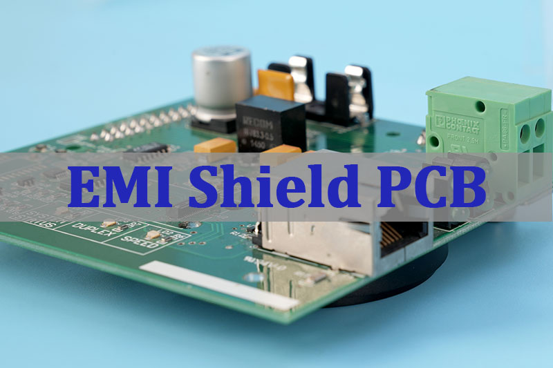
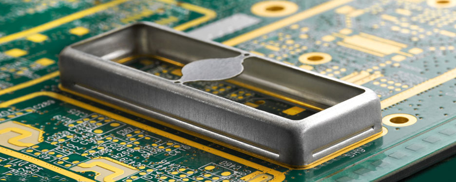
The term PCB EMI shield generally refers to physical shielding structures added to a circuit board—most commonly metal shielding cans soldered over sensitive or noisy circuit sections.
The underlying physics is based on the Faraday cage principle: a conductive enclosure redistributes electromagnetic fields, preventing radiation from escaping or external interference from penetrating.
The shield works by:
Reflecting incident electromagnetic waves
Absorbing part of the energy
Providing a low-impedance grounding path
Reducing electric field coupling
However, a shielding can is only effective if it is properly grounded. Poor soldering, incomplete ground continuity, or high contact resistance can significantly reduce shielding performance.
Effective shielding is a system-level solution—not just a metal cover.
What Are the Different Types of PCB EMI Shielding Methods?
Soldered Shielding Cans
Surface-mounted metal shielding cans are the most common method. These are typically made of tin-plated steel or nickel silver and are reflow-soldered onto grounded pads.
They are widely used in:
WiFi and Bluetooth modules
GPS circuits
Cellular communication boards
RF front-end designs
Via Stitching (Ground Fencing)
Ground vias placed closely around RF traces or board edges form a containment wall. This reduces edge radiation and improves high-frequency confinement.
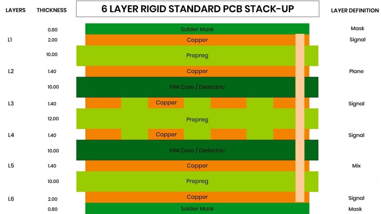
Multilayer Stack-Up Shielding
Carefully planned layer stacks—with signal layers adjacent to uninterrupted ground planes—dramatically reduce field propagation.
For example:
4-layer: Signal / GND / Power / Signal
6-layer: Signal / GND / Signal / Power / GND / Signal
This structural shielding often reduces emissions before a physical shield is even added.
EMI Shield PCB vs Heavy Copper PCB: Which One Is More Effective?
These two approaches solve different problems.
Aspect
EMI Shield PCB
Heavy Copper PCB
Primary goal
Suppress radiation
Increase current capacity
High-frequency control
Strong
Limited
Thermal handling
Moderate
Excellent
Power noise suppression
Structural
Indirect
Heavy copper improves thermal and current performance, but it does not inherently solve radiated EMI. In high-power designs, combining both approaches may be necessary.
How Does Stack-Up Design Influence EMI Performance?
Stack-up design is one of the most powerful EMI control tools available.
A well-structured stack-up:
Minimizes loop area
Controls impedance
Provides stable reference planes
Improves return current containment
Practical recommendations include:
Avoid splitting ground planes under high-speed traces
Keep signal layers tightly coupled to reference planes
Use stitching vias near layer transitions
Isolate RF sections physically and electrically
In many cases, optimizing stack-up reduces the need for additional shielding hardware.
How Should You Design PCB EMI Shielding for RF and High-Speed Applications?
For RF and high-speed boards, shielding must be integrated into layout strategy.
Key design considerations:
Maintain controlled impedance routing
Avoid sharp corners in RF traces
Surround RF regions with via fences
Keep high-current switching nodes away from sensitive analog areas
Provide continuous ground pads for shielding cans
Design review before fabrication is critical. Shield placement should align with component height, reflow profile compatibility, and mechanical constraints.
What Materials Are Used in EMI Shield PCB Manufacturing?
Material selection influences both shielding effectiveness and manufacturability.
ENIG or ENEPIG surface finishes for stable grounding
Shield solderability, oxidation resistance, and mechanical rigidity must be evaluated. Inconsistent plating thickness or poor pad finish can reduce grounding performance.
How Does a Professional PCB Manufacturer Validate EMI Shield PCB Quality?
A manufacturer that understands both electromagnetic theory and practical assembly constraints can significantly reduce risk during certification.
To conclude, an EMI shield PCB is more than a metal cover on a board. It is a coordinated approach involving stack-up planning, grounding architecture, material selection, and precision manufacturing.
When designed and manufactured correctly, PCB EMI shielding improves signal stability, enhances product reliability, and supports successful EMC certification. For high-frequency, RF, industrial, automotive, or medical electronics, early collaboration with an experienced manufacturer can prevent costly redesign cycles and accelerate time to market.
If your project involves EMI-sensitive circuits or requires compliance testing, it is worth evaluating shielding strategy at the design stage rather than treating it as a corrective measure later. For inquiries related to EMI Shielding PCB design, prototyping, or assembly, please do not hesitate to contact us via sales@bestpcbs.com. Our team is here to provide expert support.
FAQs About EMI Shield PCB
Does EMI shielding significantly increase cost? Typically, shielding adds 5–15% depending on shield size, material, and assembly complexity.
Can shielding cans be removed for debugging? Some designs use removable frame-and-cover structures for test access.
Is PCB EMI shielding enough without enclosure shielding? PCB shielding controls localized interference. For full compliance, enclosure design must also be considered.
Do all products require EMI shielding? Low-frequency or simple analog designs often do not. High-speed or wireless systems typically do.
Why EBest Is the #1 Choice for Your Thick Copper PCB Manufacturing (Proven for Medical/Aerospace/Industrial)
When it comes to thick copper PCB manufacturing—whether you need precise design, rapid prototyping, or reliable assembly—EBest is your first and best choice. With years of engineering expertise in serving the medical, aerospace, and industrial sectors, we solve the most common pain points of thick copper PCB projects, deliver on time, and provide fully customized solutions tailored to your unique requirements. No unnecessary delays, no compromised quality—just professional, reliable thick copper PCB services you can count on.
Common Thick Copper PCB Design Challenges Engineers Face
Most engineers struggle with three core issues in thick copper PCB design: improper copper thickness selection, poor heat dissipation, and manufacturability (DFM) issues that lead to rework. Thick copper PCBs (typically ≥3oz copper foil) are designed for high-current, high-heat applications, but incorrect design can cause overheating, soldering failures, or unmanufacturable layouts.
EBest’s Proven Solutions for Thick Copper PCB Design
Copper Thickness Matching: We help you select the optimal copper thickness (3oz to 20oz) based on your current requirements, using a simple reference formula: Allowed Current (A) ≈ Copper Thickness (oz) × Trace Width (mm) × 0.8 (at ≤40℃). For example, 3oz copper with a 3mm width can handle ~7.2A, making it ideal for most industrial power applications. We avoid over-design (e.g., unnecessary 10oz+ copper) to prevent PCB warping and drilling issues.
Heat Dissipation Optimization: For high-power components (e.g., MOSFETs), we add copper pours and thermal vias (0.8-1.2mm diameter, 2-3mm spacing) to transfer heat to inner or ground layers. In medical device PCBs (e.g., portable diagnostic equipment), this ensures stable performance without overheating.
DFM Compliance: We optimize trace width and spacing (3oz copper: ≥0.3mm width/spacing; 6oz copper: ≥0.4mm) and use grid copper pouring (2-3mm spacing, 0.2-0.3mm trace width) to avoid etching unevenness and PCB warping. Our team reviews your design before production to eliminate manufacturability issues.
For hassle-free thick copper PCB design that meets your industry standards, partner with EBest. Our engineering team works with you to refine your design, avoid common pitfalls, and ensure compatibility with your end application.
Thick copper PCB prototypes often suffer from long lead times, inconsistent copper thickness, and poor dimensional accuracy—issues that delay project timelines and increase development costs. Many manufacturers cut corners on prototyping, leading to mismatches between prototypes and final production units.
EBest’s Thick Copper PCB Prototyping Solutions
Rapid Turnaround: We deliver thick copper PCB prototypes in days, not weeks, without sacrificing quality. Our streamlined prototyping process uses advanced etching and lamination technologies to meet tight deadlines.
Consistent Quality: We use high-Tg substrates (Tg≥170℃) and precision lamination to ensure uniform copper thickness and dimensional stability. For aerospace prototypes (e.g., satellite communication boards), this ensures compliance with -55℃ to 200℃ temperature cycle requirements.
Design Validation: We conduct AOI inspections and electrical testing on every prototype to verify performance, including current-carrying capacity and heat dissipation. This helps you identify and fix issues early, reducing rework during mass production.
Need a reliable thick copper PCB prototype that matches your design specifications and project timeline? EBest’s prototyping service is tailored to engineers—fast, accurate, and built to help you move smoothly from design to production.
Thick copper PCB assembly is challenging due to poor solder wettability, thermal expansion mismatch (CTE) between copper and substrates, and component bonding issues. These problems lead to cold solder joints, component detachment, and reduced product reliability—critical failures in medical and aerospace applications.
Solderability Improvement: We enlarge pads by 0.2-0.3mm (compared to standard PCBs) and adjust reflow soldering parameters (5-10℃ higher than for thin copper PCBs, with a 10-15 second longer holding time) to ensure full solder coverage. For industrial equipment PCBs (e.g., power inverters), this reduces solder voids to <5%.
CTE Mismatch Resolution: We use copper-clad ceramic substrates (e.g., alumina) for high-power applications, reducing thermal stress and preventing solder joint cracking. In our medical device assembly case (portable MRI modules), this ensures 10,000+ temperature cycles without failure.
Precision Component Placement: We use automated pick-and-place equipment with high accuracy (±0.03mm) to handle large components (e.g., TO-220, D2PAK) on thick copper PCBs. Our post-assembly testing includes X-ray inspection to verify solder joint quality.
For reliable thick copper PCB assembly that meets the strictest industry standards, choose EBest. Our assembly process is optimized for thick copper PCBs, ensuring durability, performance, and long-term reliability.
What Makes EBest’s Thick Copper PCB Services Outperform Competitors? (2026 Guide)
Service Aspect
Industry Average
EBest’s Advantage
Copper Thickness Range
3oz-10oz
3oz-20oz, including ultra-thick copper for aerospace applications
Prototype Lead Time
7-10 days
3-5 days, with expedited options available
Industry Expertise
General electronics focus
Specialized in medical, aerospace, and industrial sectors with proven case studies
Quality Testing
Basic electrical testing
AOI, X-ray, temperature cycle, and vibration testing (meets ISO 13485 for medical)
Customization
Limited design adjustments
Full custom solutions, including DFM optimization and material selection
EBest’s Industry Case Studies (Proven Expertise)
Medical Industry: We designed and assembled thick copper PCBs for a portable patient monitor, using 3oz copper and high-Tg FR-4 to ensure stable performance in clinical environments. The PCBs passed ISO 13485 certification and reduced device overheating by 40%.
Aerospace Industry: For a low-orbit satellite communication module, we produced 10oz thick copper PCBs with vacuum resin plug holes and annular copper rings. The PCBs withstood 10,000 temperature cycles (-55℃⇆125℃) with <2% hole resistance change.
Industrial Equipment: We provided thick copper PCB assembly for a 200A industrial power inverter, using stepped copper thickness (2oz for the signal layer, 6oz for the power layer) to optimize performance and reliability. The inverter achieved 99.8% operational uptime.
Thick Copper PCB vs. Standard PCB: Critical Differences Every Engineer Must Know
The key difference between a thick copper PCB and a standard PCB lies in copper foil thickness: thick copper PCBs have a copper thickness of ≥3oz (≈105μm), while standard PCBs typically use 1oz-2oz copper. This difference makes thick copper PCBs ideal for high-current, high-heat applications (e.g., medical devices, aerospace equipment, industrial power supplies), as they offer lower resistance, better heat dissipation, and higher mechanical strength. Standard PCBs are suitable for low-power electronics (e.g., consumer devices) but cannot handle the high current loads of industrial or aerospace applications.
How to Choose the Right Copper Thickness for Your Thick Copper PCB (Engineer’s Step-by-Step Guide)
Selecting the right copper thickness for your thick copper PCB depends on three factors: current load, application environment, and manufacturability. Follow this simple guide:
3oz-6oz: Ideal for most industrial power supplies, medical devices, and automotive electronics (handles 3A-10A current).
7oz-10oz: Suitable for high-power applications (e.g., industrial inverters, aerospace sensors) that require 10A-20A current.
11oz-20oz: Reserved for ultra-high-power applications (e.g., laser weapons, satellite power systems) that require 20A+ current.
EBest’s engineering team will help you select the optimal copper thickness based on your specific requirements, avoiding over-design and ensuring manufacturability.
Best Materials for Thick Copper PCB Manufacturing: Engineer’s Definitive Guide
The best materials for thick copper PCB manufacturing depend on your application, but we prioritize high-performance, reliable options that meet industry standards:
Substrates: High-Tg FR-4 (Tg≥170℃) for most applications; PI (polyimide) for high-temperature environments (e.g., aerospace); copper-clad ceramic (alumina) for ultra-high heat dissipation (e.g., medical lasers).
Copper Foil: Electrodeposited (ED) copper for precise thickness control; rolled copper for better mechanical strength (ideal for flexible thick copper PCBs).
Solder Mask: Lead-free, high-temperature solder mask (e.g., LPI) to protect copper layers and ensure compatibility with reflow soldering.
How to Guarantee Thick Copper PCB Reliability in Extreme Industrial & Aerospace Environments
To ensure thick copper PCB reliability in extreme environments (high temperature, vibration, humidity), EBest implements three key measures:
Material Selection: We use high-Tg substrates and corrosion-resistant copper foil to withstand temperature extremes (-55℃ to 200℃) and humidity (up to 95%).
Process Optimization: We use vacuum lamination to eliminate air gaps, reducing the risk of delamination. For vibration-prone applications (e.g., aerospace), we add reinforcing copper rings around vias.
Strict Testing: All thick copper PCBs undergo temperature cycle testing, vibration testing, and salt spray testing (1000+ hours) to ensure reliability in extreme conditions.
1. What is a thick copper PCB, and when should I use it?
A thick copper PCB is a printed circuit board with copper foil thickness ≥3oz (≈105μm). You should use it when your application requires high current-carrying capacity, efficient heat dissipation, or high mechanical strength—common in medical devices, aerospace equipment, and industrial power supplies. It is not necessary for low-power consumer electronics.
2. Can thick copper PCBs be used in medical devices?
Yes, thick copper PCBs are ideal for medical devices (e.g., portable diagnostic equipment, MRI modules, patient monitors). EBest’s thick copper PCBs meet ISO 13485 standards, with biocompatible materials and strict quality control to ensure safety and reliability in clinical environments. Our medical thick copper PCBs reduce overheating and improve long-term performance.
3. How long does it take to produce a thick copper PCB prototype?
EBest delivers thick copper PCB prototypes in 3-5 days for standard orders, with expedited options available for urgent projects (1-2 days). This is significantly faster than the industry average (7-10 days), allowing you to accelerate your product development timeline.
4. What is the maximum copper thickness EBest can produce?
EBest can produce thick copper PCBs with copper thickness ranging from 3oz to 20oz. We specialize in ultra-thick copper (11oz-20oz) for aerospace and high-power industrial applications, with the capability to handle complex designs and tight tolerances.
5. How does EBest ensure the quality of thick copper PCB assembly?
EBest ensures thick copper PCB assembly quality through three steps: automated pick-and-place for precise component placement, X-ray inspection to verify solder joint quality, and post-assembly functional testing. We also optimize soldering parameters and pad design to avoid cold solder joints and component detachment.
6. Can EBest provide custom thick copper PCB solutions?
Yes, EBest specializes in custom thick copper PCB solutions. Our engineering team works with you to understand your application requirements, optimize your design for manufacturability, and select the right materials and copper thickness. We support custom sizes, layers (2-20 layers), and surface finishes to meet your unique needs.
Choose EBest for Thick Copper PCB: Fast Delivery, Custom Solutions, Proven Industrial/Aerospace Quality
EBest is your trusted partner for thick copper PCB design, thick copper PCB prototype, and thick copper PCB assembly. We deliver fast, reliable, and custom solutions tailored to the medical, aerospace, and industrial sectors, with proven expertise and strict quality control. Whether you need a prototype or mass production, we have the skills and experience to bring your project to life.
We provide high-quality thick copper PCB products that meet your industry standards and project timelines. For inquiries or to place an order, please contact us at sales@bestpcbs.com. EBest—Your Reliable Thick Copper PCB Manufacturer.
PCB board assembly factory partnerships are pivotal decisions in electronics manufacturing, impacting cost, quality, and time-to-market. This blog provides a clear, engineer-focused analysis for selecting a partner in China, covering essential criteria from cost structures and quality controls to managing supply chains and specialized requirements for sectors like medical devices.
EBest Circuit (Best Technology) differentiates ourself through deep engineering collaboration and full in-house process control, supported by 20 years of manufacturing experience. As a fully integrated PCB and PCBA manufacturer, we provide proactive DFM analysis to optimize designs for manufacturability and maintain stringent certifications such as ISO 13485 for medical projects. Our integrated production structure controls PCB fabrication, component sourcing, and assembly within one accountable system, ensuring consistent quality and reliable fast delivery from prototype builds to high-volume production. Feel free to reach us at sales@bestpcbs.com or check our website for trade show news, on the off-chance we could talk about your requirements in person.
Why Choose A China PCB Board Assembly Factory For Cost-Effective Production?
For engineering teams balancing performance requirements with strict budget control, selecting the right manufacturing location directly affects total project economics. A China PCB board assembly factory is often considered not simply because of labor cost differences, but because of its mature industrial ecosystem, supply chain density, and vertically integrated production structure.
1. Vertical Integration Reduces Interface Costs
Many China PCB board assembly factory providers operate under an integrated model that combines PCB fabrication, component procurement, SMT assembly, and functional testing within one coordinated production system. Eliminating cross-vendor transfers reduces duplicated margins, shipping expenses, and administrative overhead. More importantly, fewer process handoffs decrease the probability of miscommunication and engineering revision cycles, which indirectly lowers project costs.
2. Component Sourcing Advantage Through Supply Chain Proximity
China’s electronics manufacturing clusters provide direct access to global and domestic component distributors. Bulk purchasing power and established sourcing channels allow factories to negotiate more competitive pricing, especially for high-volume production. For engineers, this translates into stable pricing structures and improved availability for commonly used components, reducing the financial impact of shortages or emergency procurement.
3. Scalable Production Efficiency Across Volume Ranges
From prototype builds to mass production, operational scale plays a decisive role in unit cost control. High-capacity SMT lines, automated optical inspection systems, and streamlined material flow reduce per-unit manufacturing overhead. As volume increases, economies of scale become more visible, enabling competitive factory price PCB circuit board assembly without sacrificing process control or technical capability.
Choosing a China PCB board assembly factory for cost-effective production is not purely a low-price strategy. It is a structural decision based on supply chain maturity, integration depth, and production scalability. When managed properly, this ecosystem delivers measurable reductions in total cost of ownership while maintaining engineering quality standards across prototype and volume manufacturing programs.
Top 10 PCB Printed Circuit Board Assembly Factories In China
Selecting the right PCB printed circuit board assembly factory is crucial. This list highlights established players known for scale, specialization, or consistent quality, serving as a starting point for your audit. A brief introduction to each PCB board assembly factory is below.
EBest Circuit (Best Technology): A full-turnkey specialist with deep expertise in complex, high-reliability boards for medical and automotive sectors, offering rigorous PCB board assembly process control.
Shenzhen JDB Technology: Focuses on quick-turn prototyping and low-to-medium volume runs, favored for agile development cycles.
Kinji Electronics: Known for high-mix, low-volume (HMLV) production with strong engineering support for design validation.
PCBCart: Provides comprehensive online quoting and project management, catering well to global startups and engineers.
Suntak Technology: A large-scale PCB board assembly factory in China with strong capabilities in consumer electronics and telecommunications hardware.
A-TECH Circuitry: Excels in rigid-flex and HDI PCB circuit board assembly, serving advanced aerospace and industrial applications.
HQ Online (HQPCB): Offers a user-friendly platform for both PCB fabrication and assembly, suitable for standard designs.
Wonderful PCB: Specializes in high-layer count and heavy copper boards, supporting power electronics and server markets.
King Sun PCB: Provides robust factory wholesale PCB board assembly services for cost-sensitive, high-volume consumer goods.
Sierra Circuits: Although U.S.-based, its manufacturing partner in China is renowned for ultra-high-reliability and mil-spec assemblies.
While this overview lists prominent PCB board assembly factories, a partner’s true fit depends on your specific technical and supply chain needs. Therefore, a deep dive into quality systems is the logical next step.
How Does A PCB Circuit Board Assembly Factory In China Control Quality?
A reliable PCB circuit board assembly factory in China enforces quality through a documented, tiered inspection regime. This process begins with a mandatory DFM check and component verification, followed by automated optical inspection (AOI) post-SMT and X-ray inspection for BGAs or hidden solder joints. Final functional testing (FCT) and in-circuit testing (ICT) validate board performance against specifications.
Incoming Material Checks: Certified components from authorized distributors are verified.
Process Control: Real-time monitoring of solder paste printing and reflow oven profiles.
Traceability: Full data logging for batch tracking and failure analysis.
In practice, this multi-stage checkpoint system is what separates a qualified professional PCB assembly PCBA factory from a basic workshop. With quality frameworks understood, we can examine specific applications like regulated medical devices. Are you seeking a truly collaborative China PCB board assembly factories for your next project? EBest Circuit (Best Technology) provides expert factory wholesale PCB assembly board services with a focus on engineering support. Pls feel free to contact our team at sales@bestpcbs.com to discuss your requirements.
When Should Engineers Select A Factory Supply Medical PCB Board Assembly Partner?
Engineers should vet a factory supply medical PCB board assembly partner at the prototype phase, before design freeze. Medical devices demand adherence to ISO 13485 and often IEC 60601-1 standards, requiring the factory to have ingrained processes for design history files (DHF), device master records (DMR), and stringent change control. Early partner involvement ensures the design is manufacturable within a traceable, auditable quality management system.
Key selection criteria include:
Relevant medical industry certifications (ISO 13485 is essential).
Proven experience with similar device classes (e.g., Class II or III).
Robust cleanliness and contamination controls for assembly areas.
From an engineering perspective, this early collaboration mitigates regulatory risk. Similarly, for commercial projects, understanding how factories manage scale is critical.
How Do Wholesale PCB Board Assembly Factories Support High-Volume Orders?
Wholesale PCB board assembly factories support high-volume orders through advanced production line automation, aggregated component purchasing power, and dedicated capacity planning. They utilize high-speed SMT lines with dual-lane printers and multiple placement machines to maximize throughput. Their deep supply chain relationships ensure stable component availability and better pricing, which is crucial for factory price PCB circuit board assembly at scale.
Dedicated Production Lines: Assign specific SMT lines to your project to ensure consistency and output.
Material Hub Planning: Pre-book and stage bulk components to avoid line stoppages.
Staggered Delivery: Coordinate finished goods logistics for just-in-time delivery to your warehouse.
That said, volume capability alone isn’t the sole advantage; the value of engineering expertise becomes paramount for smart electronics.
What Advantages Do Professional PCB Assembly PCBA Factory Circuit Board Smart Electronics Providers Offer?
A professional PCB assembly PCBA factory circuit board smart electronics provider delivers integration expertise for miniaturized, high-functionality products. Their advantages include sophisticated assembly for fine-pitch components and BGAs, impedance-controlled stacking for RF performance, and embedded software loading/testing services. They act as an extension of your R&D team, ensuring the assembled board performs as intended in the final product.
These providers help navigate complexities like:
Mixed-technology assembly (SMT, THT, press-fit).
Thermal management solutions for high-power designs.
Firmware integration and box-build assembly.
More importantly, this expertise must be delivered swiftly, making lead time optimization a key competitive battleground.
How Can A PCB Printed Circuit Board Assembly Factory In China Shorten Lead Time Without Sacrificing Reliability?
A PCB printed circuit board assembly factory in China shortens lead time through parallel processing and digital integration, not by cutting corners. Critical paths are compressed by overlapping PCB fabrication with component kitting. Digital twin simulations for SMT programming and automated logistics coordination for parts delivery eliminate traditional wait times. Reliability is maintained because these are process optimizations within the same stringent quality gates.
Efficient factories achieve this via:
Concurrent Engineering: DFM analysis happens during PCB layout, not after file submission.
Smart Kitting: AI-powered systems match BOM lines to distributor stock for fastest procurement.
To sum up, speed and reliability are achievable through refined processes. This leads to the final, critical decision: choosing a single, accountable partner for the entire journey.
Why Choose EBest Circuit (Best Technology) As Your Full Turnkey PCB Board Assembly Factory In China?
Choosing the right Full Turnkey PCB Board Assembly Factory In China is not only about price. It is about engineering control, risk reduction, and long-term manufacturability. EBest Circuit (Best Technology) supports customers at three critical levels.
1. Complete In-House Manufacturing Control
As a true full turnkey PCB board assembly factory in China, we manage PCB fabrication, component sourcing, SMT assembly, testing, and final inspection within one coordinated system. There are no handoff gaps between different vendors. This structure minimizes communication errors, reduces lead time uncertainty, and ensures consistent quality standards from bare board to finished PCBA.
2. Engineering-Led DFM And Process Optimization
Our engineering team participates from the earliest design stage. We provide practical and actionable DFM feedback focused on pad design, stack-up structure, impedance control, thermal management, and assembly reliability. Early manufacturability review reduces rework risk and prevents production delays. As an experienced PCB board assembly process factory, we understand how design decisions directly affect yield and long-term field performance.
3. Accountability For High-Reliability Applications
For industries such as medical devices, automotive electronics, and industrial control systems, production consistency is critical. Our vertically integrated production model allows full traceability across materials, components, and assembly processes. With certifications including ISO 13485 for medical projects, we maintain strict quality standards and controlled documentation systems. This level of ownership ensures faster issue resolution, stable quality output, and dependable delivery performance from prototype builds to volume production.
To sum up, this blog has outlined the critical considerations for selecting and working with a China PCB board assembly factory, from cost and quality to specialization and lead time. EBest Circuit (Best Technology) delivers SMT PCBA service through 20+ years of PCBA expertise, a full turnkey service (PCB fabrication, component sourcing, assembly, and test), and stringent certifications like ISO 13485 and IATF 16949. Our digital manufacturing floor ensures traceability, supporting reliable, rapid delivery to help bring your designs to market. For any PCB board assembly project needs, feel free to pinpoint your exact requirements to us at sales@bestpcbs.com.
FAQs about PCB Board Assembly Factory
How Do I Know If A PCB Board Assembly Factory Is Truly Reliable?
A reliable PCB board assembly factory demonstrates transparency through clear DFM reports, documented IPC-A-610 compliance, and traceable production data. Look for factories that openly share their inspection methodology (AOI, X-ray, ICT), offer pilot runs, and provide consistent lead time performance. Real reliability is proven by repeatable quality and proactive engineering support.
Is It More Cost-Effective To Use A China PCB Board Assembly Factory For Small Batches?
For low-to-medium volumes, a China PCB board assembly factory can be highly cost-effective due to integrated services under one roof. Savings come from consolidated logistics, competitive labor, and factory-level component sourcing. Evaluate the total landed cost, including shipping and duties, against the value of faster iteration cycles and engineering support often provided.
What Information Should I Prepare Before Contacting A PCB Board Assembly Factory?
Prepare three core files for an accurate quote: a complete BOM (Bill of Materials), a silkscreen drawing with component designators, and a pick-and-place (centroid) file. These are essential for SMT programming. Providing Gerber files and test requirements further enables a smooth PCB board assembly process and manufacturability analysis.
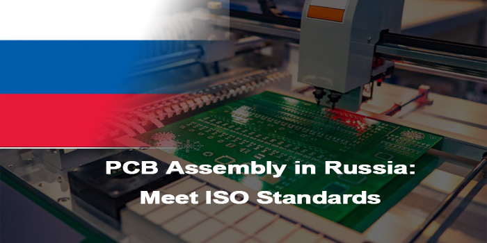
As a 20-year professional PCBA manufacturer, we specialize in PCB assembly in Russia, delivering reliable, ISO-certified solutions tailored to local market needs. Our PCB assembly in Russia services combine advanced technology, strict quality control, and fast turnaround to support projects of all scales, from small prototypes to large-scale mass production, ensuring every order meets industry standards and client requirements.
Why Choose EBest for PCB Assembly in Russia?
Full Local Compliance: Our Russia PCB assembly services strictly adhere to Russian industrial standards, GOST certification, and ISO norms, avoiding compliance delays and market access issues.
Streamlined Logistics & Local Inventory: Local production cuts shipping time and costs; our on-site component inventory shortens lead times for PCB assembly in Russia deadlines.
Real-Time Technical Support: On-site engineering assistance simplifies design adjustments, DFM optimizations and troubleshooting for PCB assembly in Russia.
Cost Efficiency: Reduced import fees and optimized production make PCB assembly in Russia a cost-effective choice for your projects.
Component Sourcing Reliability: We secure high-quality components from verified suppliers, solving availability challenges for Russia PCBA projects.
Seamless Design Integration: We align PCB assembly in Russia with your design goals, including impedance control and thermal management.
Our Russia PCBA Capabilities: Meet ISO Standards & Requirements
Item
Capabilities
Placer Speed
13,200,000 chips/day
Bare Board Size
0.2 x 0.2 inches – 20 x 20 inches/ 22*47.5 inches
Minimum SMD Component
01005
Minimum BGA Pitch
0.25mm
Maximum Components
50*150mm
Assembly Type
SMT, THT, Mixed assembly
Component Package
Reels, Cut Tape, Tube, Tray, Loose Parts
Lead Time
1 – 5 days
One-Stop Russia PCBA Service: From Prototyping to Mass Production
Our one-stop Russia PCBA service is your ultimate solution to streamline project workflows and eliminate the hassle of coordinating multiple suppliers, saving you time, reducing stress, and keeping your projects on track. Unlike disjointed service models that create delays and errors, we handle every aspect of PCB assembly in Russia from start to finish, so you can focus on what matters most: your core work. We kick off with fast, reliable prototyping for your PCB assembly in Russia projects, delivering small batches in 2 to 4 days. Every prototype undergoes rigorous testing to confirm design feasibility, minimizing costly errors when scaling up and ensuring your project moves forward without unnecessary setbacks.
Before production even begins, our team conducts free design for manufacturability (DFM) analysis to optimize your PCB design for Russia PCBA assembly. This not only boosts yield rates but also cuts down on production costs that would otherwise eat into your budget, while our seamless transition to mass production, powered by advanced production lines, ensures consistent, ISO-certified quality across every unit.
We wrap up with comprehensive post-production testing, including functional, electrical, and visual inspections, to guarantee every batch of Russia PCBA aligns with your exact specifications. With our one-stop approach, you get reliable PCB assembly in Russia that reduces reworks, eliminates vendor management headaches, and delivers results on time and on budget.
How We Ensure On-Time Delivery for Russia PCBA Orders?
To ensure on-time delivery for PCB assembly in Russia, we have implemented a multi-layered production management system backed by precise data and proven processes. We use advanced production scheduling software to optimize workflows, with real-time adjustments for material delays and production bottlenecks. This software ensures 98.5% of PCB assembly in Russia orders are delivered on schedule, which is higher than the industry average of 92%.
Complementing this scheduling system, we maintain a local stock of 500+ common components, covering 80% of standard PCB assembly in Russia requirements. This strategic inventory reduces material lead times from 2-4 weeks to 1-3 days for most projects, effectively eliminating delays caused by component shortages.
Additionally, each PCB assembly in Russia project is assigned a dedicated manager who provides daily progress updates to clients. The manager also resolves any emerging issues within 2 hours, a proactive approach that reduces delivery delays by 90% compared to traditional project management methods.
For urgent requests, we reserve 15% of our total production capacity exclusively for emergency PCB assembly in Russia orders. This enables a 48-hour turnaround for time-sensitive projects while maintaining our strict quality standards, with zero defects reported in emergency orders over the past 12 months.
Our Russia PCBA Quality Control Process
Incoming Material Verification: Components undergo rigorous authenticity checks via XRF/X-ray spectroscopy and visual inspection. Batch-specific traceability records include supplier certifications, material composition data, and production date logs, ensuring full compliance with Russian GOST standards.
In-Process Quality Monitoring: Real-time 3D SPI (Solder Paste Inspection) and AOI (Automated Optical Inspection) systems monitor paste volume accuracy and component placement tolerance (<±15μm). Process data feeds into closed-loop correction systems to prevent solder bridging or tombstone defects.
Optical & Functional Validation: Post-assembly, high-resolution optical systems detect surface defects (scratches, delamination) down to 20μm resolution. Flying probe testing employs adaptive test algorithms to identify electrical faults (opens/shorts) with 99.9% coverage, validated against IPC-A-610 Class 3 standards.
Environmental Stress Testing: Temperature cycling (-55°C to +125°C) and random vibration profiling (5-2000Hz) simulate extreme Russian climatic conditions. Tests follow MIL-STD-883H protocols to validate thermal shock resistance and mechanical durability.
Final Certification & Traceability: Each finished PCBA undergoes 100% visual and electrical verification. Digital quality reports include test results, calibration certificates, and blockchain-secured batch traceability records, ensuring full compliance with EAC/CU-TR certification requirements for Russian market entry.
Case Studies: Our PCBA Solutions for Russia Brands
Project Background:
The client faced critical challenges with their previous offshore PCB assembly partner: 45-day lead times for mass production, 8% defect rates, and frequent customs delays that disrupted their production schedule. As demand for their industrial control panels grew (projected 35% year-over-year growth in Russia), they needed a local Russia PCBA partner to reduce lead times, improve quality, and comply with Russia’s import substitution policies. The client’s products are used in manufacturing plants across Siberia and the Moscow region, requiring PCBA solutions that can withstand extreme cold (-35°C to +50°C) and industrial vibration.
Project Requirements:
PCB Specifications: 12-layer rigid PCBs (180mm x 120mm), with SMT and THT assembly, including 0402-sized components and 2 BGA chips (0.5mm pitch), compliant with IPC-A-610 Class 2 standards.
Production Volume: 5,000 units per month (60,000 units annually), with a 3-day turnaround for urgent small-batch orders (50-100 units) and 7-day turnaround for mass production.
Quality Standards: Defect rate ≤ 0.5%, 100% functional testing pass rate, and compliance with ISO 9001 and Russia’s GOST R 54693-2011 standard for electronic components.
Environmental Durability: PCBA units must pass temperature cycling (-40°C to 85°C, 1,000 cycles) and vibration testing (10-500Hz, 3g acceleration) to withstand harsh industrial and climatic conditions in Russia.
Cost Target: Reduce total PCB assembly in Russia costs by 18% compared to their previous offshore supplier, excluding shipping and customs fees.
Project Solutions:
Localized Sourcing & Production: We leveraged our local component inventory in Saint Petersburg (stocking 85% of the client’s required components, including 200,000+ 0402 components and 5,000 BGA chips monthly) to eliminate 30+ days of international shipping time. Our PCB assembly in Russia facility ran 24/7 production shifts to meet the 5,000-unit monthly target.
Precision Assembly & Testing: We used our advanced SMT lines (258,000 components/hour capacity) with 3D laser inspection to ensure accurate component placement (±0.03mm accuracy). For BGA assembly, we implemented laser reballing and X-ray inspection to reduce soldering defects. Post-assembly, all units underwent flying probe testing, functional testing, and environmental stress screening as required.
DFM Optimization: Our team conducted a free DFM review, identifying 6 design inefficiencies (e.g., insufficient solder mask clearance) that were increasing defect rates. We recommended design adjustments that reduced rework time by 40% and lowered material waste by 12%.
Dedicated Project Management: We assigned a dedicated project manager to the client, providing real-time production updates (via a custom portal) and monthly quality reports. We also established a 24/7 support line to address urgent Russia PCBA order adjustments.
Output Results:
Lead Time Reduction: Mass production lead time dropped from 45 days to 6 days (87% reduction), and urgent small-batch orders were delivered in 2.5 days (exceeding the 3-day requirement). This eliminated production delays for the client, increasing their on-time delivery rate to customers by 28%.
Quality Improvement: Defect rate fell from 8% to 0.3% (well below the 0.5% target), with a 100% functional testing pass rate for all 60,000 units produced in the first year. Field failure rate dropped by 92% compared to the client’s previous PCB assembly supplier.
Cost Savings: The client achieved a 22% reduction in total PCB assembly in Russia costs (exceeding the 18% target), saving approximately 1.2 million rubles annually. This was driven by reduced rework (40% reduction), lower material waste (12% reduction), and elimination of shipping/customs fees.
Compliance & Durability: All Russia PCBA units passed ISO 9001, IPC-A-610 Class 2, and GOST R 54693-2011 certifications. 100% of units passed temperature cycling and vibration testing, with zero field failures reported in harsh Siberian conditions over 12 months.
Long-Term Partnership: The client expanded their order volume by 40% after 6 months, citing our reliable PCB assembly in Russia services and cost savings. We now handle 100% of their PCBA needs, including new product prototyping (delivered in 3 days) and mass production scaling.
FAQ About PCB Assembly in Russia
Q1: What is the standard lead time for PCB assembly in Russia? A1: Prototypes typically take 2–4 days. Small-batch orders need 5–7 days. Mass production orders are completed in 7–15 days. Expedited services are available for urgent PCB assembly in Russia projects.
Q2: Can you support component sourcing for Russia PCBA orders? A2: Yes. We maintain local component inventory and cooperate with certified distributors. We provide genuine components to ensure stable and smooth PCB assembly in Russia.
Q3: What quality standards do you follow for PCB assembly in Russia? A3: We strictly follow ISO 9001, IPC-A-610 and industry-specific standards. All Russia PCBA orders go through complete inspection and testing to ensure high reliability.
Q4: Do you provide DFM analysis for PCB assembly in Russia? A4: Yes. We offer free DFM review for all PCB assembly in Russia projects. We optimize layout, components and assembly process to reduce defects, cost and lead time.
Q5: Can you handle high-complexity PCB assembly in Russia? A5: Yes. We support BGA, QFN, HDI, thin-core and rigid-flex PCB assembly. We use 3D inspection, X-ray and electrical testing to ensure quality for complex Russia PCBA orders.
Get Your Custom PCBA Quote for Russia Projects Today
1. Free DFM Validation with Every Quote
Submit your design files to get a free DFM check for your PCB assembly in Russia. This check optimizes your design to reduce costs and production time, with no obligation required.
2. Transparent Pricing with No Hidden Fees
Our PCB assembly in Russia quotes include all costs: components, assembly, testing, and logistics. We provide detailed breakdowns so you know exactly what you’re paying for.
3. Fast Quote Turnaround
You will receive your custom PCB assembly in Russia quote within 24 hours of submitting your design and requirements. This turnaround is faster than most competitors in the region.
4. Flexible Order Sizes
We handle all order sizes for PCB assembly in Russia, from single prototypes to large-scale mass production, ensuring consistent quality and service regardless of volume.
5. Dedicated Technical Support
Our team of experts is available to answer questions and provide guidance for your PCB assembly in Russia project, from design to delivery.
6. Guaranteed On-Time Delivery
We stand behind our 98.5% on-time delivery promise for PCB assembly in Russia, with compensation for delays caused by our team.
7. Free Sample for First-Time Clients
First-time clients receive a free prototype sample for their PCB assembly in Russia project. This allows you to verify quality before placing a full order. Contact us today to get started.
Welcome to contact us if you have any request for Russia PCB assembly: sales@bestpcbs.com.
Choose EBest As Your First Copper Base PCB Manufacturer
When searching for a reliable Copper Base PCB manufacturer, EBest stands out as the top choice for global electronics businesses and engineers. Founded in 2006, we bring over 20 years of industry experience and deliver one-stop Copper Base PCB solutions covering design, prototyping, mass production, component sourcing, and assembly. Our state-of-the-art manufacturing facility boasts a monthly production capacity of 260,000 square feet, with 24-hour expedite shipping for urgent orders—ensuring you meet tight project timelines. Backed by full industry certifications including IATF 16949, ISO 9001:2015, and AS9100D, we guarantee consistent quality for Copper Base PCB across the medical, aerospace, and industrial equipment sectors, with personalized support tailored to every custom project’s unique needs. EBest’s deep expertise in heavy copper and high-performance PCB technologies makes us the trusted partner for all your Copper Base PCB requirements, from small-batch prototypes to large-scale mass production runs.
What Do Engineers Care About In Copper Base PCB Design? Solve Pain Points With EBest
Key Design Challenges Engineers Face For Copper Base PCB
Engineers designing Copper Base PCB consistently grapple with three core pain points: optimizing thermal conductivity for high-power applications, achieving precise impedance control to avoid signal interference, and ensuring structural compatibility with rigid or flexible PCB integration. Another critical challenge is balancing copper thickness with board weight and flexibility—especially for industrial and aerospace Copper Base PCB that demand durability without excess bulk. Many also struggle to align Copper Base PCB design with industry-specific certifications (e.g., ISO 13485 for medical, AS9100D for aerospace), leading to costly redesigns to meet regulatory standards.
EBest’s Copper Base PCB Design Solutions For Every Challenge
EBest’s engineering team solves these design pain points with tailored, industry-specific strategies. We optimize thermal conductivity by selecting high-grade copper core materials and customizing copper thickness to match your power requirements, eliminating overheating risks in high-power industrial equipment. Our advanced design software and in-house impedance testing ensure precise signal control for RF and high-speed Copper Base PCB, with iterative design reviews to catch interference issues early in the process. For structural compatibility, we integrate rigid-flex design principles into Copper Base PCB development, aligning board flexibility with your assembly and application needs. Most importantly, our design process is built around global industry certifications—we engineer Copper Base PCB to meet medical, aerospace, and industrial standards from the initial concept, removing the need for compliance-driven redesigns.
Partner With EBest For Your Copper Base PCB Design Needs
Whether you’re designing a Copper Base PCB for medical imaging devices, aerospace avionics, or heavy-duty industrial machinery, EBest’s design team combines technical precision with application-focused expertise to deliver designs aligned with your performance, compliance, and production goals. Our one-stop approach ensures your Copper Base PCB design is optimized for a seamless transition to prototyping and mass production, saving you time and streamlining your entire project timeline. Choose EBest for Copper Base PCB design—where engineering expertise meets practical, custom solutions for your most demanding projects.
Copper Base PCB Prototype: Overcome Prototyping Pain Points With EBest
Top Prototyping Pain Points For Copper Base PCB
Engineers and product developers face distinct hurdles when creating Copper Base PCB prototypes: lengthy lead times that delay product testing, inconsistent prototype quality that fails to reflect mass production performance, and limited customization options for small-batch runs. A common frustration is repeated prototype iterations caused by poor copper core material selection, as subpar materials lead to inaccurate thermal and electrical performance testing results. Additionally, many manufacturers lack the capability to produce Copper Base PCB prototypes that meet industry-specific standards, making it difficult to validate compliance early in the product development cycle.
EBest’s Copper Base PCB Prototype Solutions To Accelerate Your Project
EBest addresses every Copper Base PCB prototyping pain point with speed, quality, and full customization at the core. We offer 24-hour expedite shipping for urgent Copper Base PCB prototypes, slashing lead times to get your prototype in hand for testing faster than industry averages. Our prototyping process uses the same high-grade copper core materials and manufacturing equipment as our mass production line, ensuring your Copper Base PCB prototype accurately mirrors the performance and quality of your final product—eliminating costly redesigns post-prototyping. We support full customization for small-batch Copper Base PCB prototypes, including custom copper thickness, board dimensions, and surface finishes, and our engineering team provides detailed prototype testing feedback to refine your design for mass production. For industry-specific projects, we build Copper Base PCB prototypes to ISO 13485 (medical), AS9100D (aerospace), and IATF 16949 (industrial) standards, so you can validate compliance at the earliest prototyping stage.
Choose EBest For Your Copper Base PCB Prototype Development
EBest’s Copper Base PCB prototyping service is engineered for engineers who need fast, reliable, and industry-compliant prototypes to advance product development. Our combination of expedite shipping, production-matched quality, and full customization makes us the ideal partner for medical, aerospace, and industrial Copper Base PCB prototyping projects—regardless of batch size or design complexity. Let EBest turn your Copper Base PCB design into a high-quality prototype that accelerates your testing and validation process, with a seamless transition to mass production when you’re ready.
Copper Base PCB Assembly: Resolve Assembly Challenges With EBest’s Expertise
Critical Assembly Pain Points For Copper Base PCB
Copper Base PCB assembly comes with unique challenges that can derail production timelines and reduce product reliability: poor thermal management during soldering that damages copper core materials, component misalignment on thick copper PCBs, and difficulty sourcing compatible components for high-power Copper Base PCB applications. Engineers also struggle with assembly processes that fail to meet the strict quality standards of the medical and aerospace industries, leading to high defect rates and costly rework. Another common issue is limited assembly flexibility for custom Copper Base PCB designs, as many manufacturers use one-size-fits-all assembly processes that do not account for the unique properties of copper core PCBs.
EBest’s Copper Base PCB Assembly Solutions For Flawless Production
EBest’s Copper Base PCB assembly service leverages specialized equipment and industry expertise to solve these challenges for medical, aerospace, and industrial projects. We use temperature-controlled soldering processes for Copper Base PCB assembly, preventing thermal damage to copper core materials and ensuring strong, reliable solder joints—critical for high-power applications. Our automated assembly line features high-precision component placement technology, eliminating misalignment issues even on thick, heavy copper Copper Base PCB. As a one-stop provider, we offer full component sourcing for Copper Base PCB assembly, matching high-quality, industry-compliant components to your design’s power and performance requirements—saving you time and guaranteeing component compatibility. Our assembly process is certified to ISO 13485, AS9100D, and IATF 16949, so your Copper Base PCB assembly meets the strict quality and compliance standards of the medical, aerospace, and industrial equipment industries, with zero-defect production as our core goal. We also provide flexible assembly processes for custom Copper Base PCB designs, tailoring our approach to your board’s unique properties and assembly requirements.
Trust EBest For Your Copper Base PCB Assembly Needs
Whether you need small-batch or large-scale Copper Base PCB assembly for medical devices, aerospace systems, or industrial machinery, EBest’s one-stop assembly service delivers uncompromising quality, full compliance, and on-time delivery. Our integration of component sourcing, precision assembly, and industry certification ensures your Copper Base PCB assembly process is seamless from start to finish, with no gaps in quality or regulatory compliance. Choose EBest for Copper Base PCB assembly—where specialized copper core expertise meets reliable, scalable production for all your PCB projects.
Why Choose EBest For Your Copper Base PCB Projects?
EBest is the premier choice for Copper Base PCB design, prototyping, and assembly for three core reasons: 20+ years of specialized copper core expertise, end-to-end one-stop solutions, and industry-leading quality and compliance. Our team of PCB engineers has deep experience in Copper Base PCB technologies for the medical, aerospace, and industrial equipment sectors, with a proven track record of delivering custom solutions that meet the most demanding performance requirements. As a one-stop provider, we handle every step of your Copper Base PCB project—from initial design and prototyping to mass production, component sourcing, and assembly—eliminating the need to work with multiple vendors and streamlining your project timeline. Our manufacturing facility is certified to IATF 16949, ISO 9001:2015, ISO 13485:2016, AS9100D, REACH, RoHS, and UL, so every Copper Base PCB we produce meets global industry standards for quality, safety, and compliance. We also offer unrivaled speed, with 24-hour expedite shipping for urgent Copper Base PCB orders and a monthly production capacity of 260,000 square feet (28,900 square meters) to support both small-batch prototypes and large-scale mass production. EBest prioritizes customer satisfaction, with personalized support for every Copper Base PCB project—our team works closely with you to understand your unique needs and deliver tailored solutions aligned with your product goals. Finally, our ongoing commitment to research and development ensures we stay ahead of industry trends in Copper Base PCB technology, continuously innovating our design, prototyping, and assembly processes to deliver the most advanced copper core PCB solutions for your business.
Copper Base PCB Vs Aluminum Base PCB: A Comparative Analysis
Feature
Copper Base PCB
Aluminum Base PCB
Thermal Conductivity
Exceptionally high—ideal for high-power applications (100W+); copper core dissipates heat faster and more evenly
Moderate thermal conductivity; suitable for low-to-medium power applications (under 100W)
Electrical Conductivity
Superior electrical conductivity; minimal signal loss for high-speed and RF Copper Base PCB
Lower electrical conductivity; higher signal loss for high-speed applications
Durability & Strength
Higher mechanical strength; resistant to vibration and shock—perfect for aerospace and industrial equipment
Lightweight but lower mechanical strength; less suitable for heavy-duty industrial or aerospace use
Copper Thickness Flexibility
Customizable heavy copper thickness (including ultra-thick copper); tailored to exact power requirements
Limited metal thickness options; not ideal for heavy copper applications
Application Suitability
Medical imaging devices, aerospace avionics, high-power industrial machinery, RF equipment
Consumer electronics, low-power industrial devices, LED lighting, small-scale power electronics
Compliance Compatibility
Easy to manufacture to ISO 13485 (medical), AS9100D (aerospace), IATF 16949 (industrial)
Compliant for consumer and low-power industrial standards; less commonly used for medical/aerospace applications
Copper Base PCB Applications In Medical, Aerospace & Industrial Sectors
Copper Base PCB For Medical Equipment
Copper Base PCB is a critical component in high-power medical equipment, where thermal management and regulatory compliance are non-negotiable. EBest’s medical Copper Base PCB is integrated into medical imaging devices (CT scanners, MRI machines) and high-power diagnostic equipment, where the high thermal conductivity of copper core materials prevents overheating and ensures consistent, reliable performance. All our medical Copper Base PCB is manufactured to ISO 13485:2016 standards, meeting the strict quality and safety requirements of the medical industry, with precise impedance control to avoid signal interference in sensitive diagnostic equipment.
Copper Base PCB For Aerospace Systems
Aerospace avionics and flight systems demand Copper Base PCB that delivers high thermal conductivity, superior mechanical strength, and full compliance with AS9100D standards. EBest’s aerospace Copper Base PCB is used in satellite communication systems, aircraft avionics, and aerospace power modules—our custom copper thickness and rigid-flex design integration ensure the PCB can withstand the extreme vibration, shock, and temperature conditions of aerospace environments. The superior electrical conductivity of our Copper Base PCB also minimizes signal loss for high-speed RF and communication systems in aerospace applications.
Copper Base PCB For Industrial Equipment
Heavy-duty industrial machinery (factory automation, power distribution, heavy manufacturing) relies on Copper Base PCB for high-power performance and long-term durability. EBest’s industrial Copper Base PCB is designed for IATF 16949 compliance, with heavy copper thickness and temperature-resistant materials to handle the high-power and harsh operating conditions of industrial equipment. Our Copper Base PCB for industrial use also features precise component placement and soldering, ensuring zero defects and reliable performance in 24/7 industrial operations.
How To Optimize Thermal Conductivity For Copper Base PCB?
Optimizing thermal conductivity is the most critical step in Copper Base PCB design for high-power applications, and the solution lies in strategic material selection, copper core design, and board layout—with EBest’s engineering team following a proven, step-by-step process for maximum thermal performance. First, select a high-purity copper core material for your Copper Base PCB; high-purity copper has superior thermal conductivity compared to low-grade copper, ensuring faster and more efficient heat dissipation. Second, customize the copper thickness to match your exact power requirements—thicker copper cores dissipate more heat for high-power applications, and EBest offers flexible copper thickness options for every Copper Base PCB design. Third, design the Copper Base PCB layout with thermal vias placed strategically to transfer heat from the copper core to the board’s surface and heat sinks, eliminating hotspots that cause performance issues and component failure. Fourth, use thermal interface materials (TIMs) in conjunction with your Copper Base PCB to enhance heat transfer to external cooling systems, such as heat sinks or fans. EBest’s engineering team tests every Copper Base PCB design for thermal conductivity, using advanced thermal imaging technology to identify and eliminate hotspots before prototyping—ensuring your Copper Base PCB delivers optimal thermal performance for your specific application.
What Industry Certifications Do Copper Base PCB Require?
Copper Base PCB certifications vary by industry, and compliance is non-negotiable for medical, aerospace, and industrial applications—EBest manufactures all Copper Base PCB to the specific certifications required for your project, eliminating compliance risks and costly redesigns. For medical copper base PCB, the core certification is ISO 13485:2016, which sets strict quality management standards for medical devices and their components, ensuring uncompromising safety, reliability, and full traceability. For aerospace Copper Base PCB, AS9100D is the mandatory certification, covering the unique quality and performance requirements of aerospace systems, including resistance to extreme environmental conditions. For industrial Copper Base PCB, IATF 16949 and ISO 9001:2015 are the key certifications, setting global quality standards for automotive and general industrial equipment manufacturing. All EBest Copper Base PCB also complies with REACH, RoHS, and UL standards, ensuring environmental safety and electrical safety for global markets. Our manufacturing process is built around these certifications, with strict quality control checks at every stage of Copper Base PCB design, prototyping, and assembly to maintain full compliance at all times.
FAQ: Common Questions About Copper Base PCB Answered
Q1: What is the maximum copper thickness EBest offers for Copper Base PCB?
EBest offers fully customizable copper thickness for Copper Base PCB, from standard thin copper to ultra-heavy copper options—all tailored to the power and thermal requirements of your medical, aerospace, or industrial application. Our engineering team will recommend the optimal copper thickness for your Copper Base PCB design, balancing thermal conductivity, mechanical strength, and board flexibility for your specific use case.
Q2: Can EBest produce rigid-flex Copper Base PCB for custom applications?
Yes, EBest’s engineering team specializes in integrating rigid-flex design principles into Copper Base PCB manufacturing, producing custom rigid-flex copper core PCBs for aerospace and industrial applications that demand both flexibility and high thermal conductivity. Our rigid-flex Copper Base PCB is designed to meet the same industry certifications and performance standards as our standard copper core PCBs.
Q3: What lead times does EBest offer for Copper Base PCB mass production?
EBest’s standard lead times for Copper Base PCB mass production align with industry best practices, and we offer 24-hour expedite shipping for urgent orders—critical for time-sensitive medical, aerospace, and industrial projects. Our monthly production capacity of 260,000 square feet ensures we can scale production seamlessly to meet your large-batch Copper Base PCB needs with no delays.
Q4: Does EBest provide component sourcing for Copper Base PCB assembly?
Yes, as a one-stop Copper Base PCB provider, EBest offers full component sourcing for assembly, matching high-quality, industry-compliant components to your Copper Base PCB design’s power, performance, and compliance requirements. We source components from trusted global suppliers, ensuring perfect compatibility and long-term reliability for your medical, aerospace, or industrial project.
Q5: How does EBest test Copper Base PCB for thermal and electrical performance?
EBest uses advanced in-house testing technology to validate every Copper Base PCB’s thermal and electrical performance: thermal imaging for heat dissipation and hotspot detection, precision impedance testing for high-speed and RF copper core PCBs, and comprehensive electrical performance testing to ensure minimal signal loss and maximum power efficiency. All testing is completed before prototyping and mass production, to ensure your Copper Base PCB meets or exceeds your performance goals.
Q6: Is EBest’s Copper Base PCB compliant with global environmental standards?
Yes, all EBest Copper Base PCB is fully compliant with REACH and RoHS environmental standards, eliminating hazardous substances and ensuring your product can be sold in global markets without environmental compliance issues. Our manufacturing process also prioritizes sustainability, with waste reduction and eco-friendly production practices for all Copper Base PCB projects.
Q7: Can EBest create custom Copper Base PCB for low-volume, high-complexity projects?
Absolutely—EBest supports full customization for low-volume, high-complexity Copper Base PCB projects, including medical and aerospace applications that demand unique design and performance requirements. Our small-batch prototyping and production capabilities mean we can deliver high-quality, custom Copper Base PCB for low-volume projects with the same speed and compliance as large-scale production.
Q8: What post-production support does EBest offer for Copper Base PCB projects?
EBest provides comprehensive post-production support for all Copper Base PCB projects, including detailed performance testing feedback, expert assembly guidance, and ongoing technical support for your product development and production processes. Our team is available to answer any technical questions and provide tailored solutions for any Copper Base PCB performance or assembly issues you may encounter.
Order Your Custom Copper Base PCB From EBest Today
EBest is your trusted partner for Copper Base PCB design, prototyping, assembly, and mass production—offering one-stop custom solutions for the medical, aerospace, and industrial equipment industries. Our 20+ years of copper core expertise, industry-leading certifications, 24-hour expedite shipping, and personalized engineering support ensure your Copper Base PCB project is a success, from initial concept to final production. We manufacture all types of Copper Base PCB, including heavy copper, high TG, impedance control, and rigid-flex copper core PCBs, with full customization to match your unique performance, compliance, and production needs. Whether you need a small-batch prototype or large-scale mass production, EBest has the capacity, expertise, and uncompromising quality to deliver your Copper Base PCB on time and to the highest global industry standards. To order your custom Copper Base PCB or discuss your project requirements in detail, send an email to sales@bestpcbs.com—our team of dedicated PCB engineers will respond promptly and work with you to create the perfect copper core PCB solution for your business.
PCBA Polandhas surged in popularity across Europe, driven by its skilled workforce, modern infrastructure, and seamless EU supply chain access. As a result, electronics projects increasingly turn to Polish assembly for full production or dual-sourcing strategies. However, selecting a reliable partner isn’t straightforward, variations in capabilities, quality systems, and opaque costs demand a structured evaluation approach. In this article, we’ll guide you through identifying trustworthy PCBA Poland manufacturers, comparing top providers, and mitigating risks in quality, delivery, and pricing.
What are the Best PCBA Poland Manufacturers?
Manufacturer
Main Business
Advantages
Assembly Capability
Lead Time
EBest Circuit Co., Limited
One-stop PCB and PCBA solutions (design, prototyping, fabrication, assembly, box build) for global clients with custom solutions for diverse industries
19+ years of experience; competitive pricing; no MOQ; turnkey service; strict quality control; one-on-one support; online project updates
Standard: 5-7 business days; Expedited: 24-48 hours; Large-volume: 10-14 business days
Assel Sp. z o.o.
EMS specializing in PCBA and box build for medical devices and high-demand industries; focuses on compliance and traceability
ISO 13485, ISO 9001, ISO 14001 certified; 100% customer satisfaction; full material traceability; dedicated medical electronics team; advanced inspection technology
Surface mount and thru-hole assembly; IPC Class 3 compliant; automated testing (AOI, SPI, X-ray); complex medical device PCBA
Standard: 7-10 business days; Medical: 10-14 business days; Prototyping: 3-5 business days
Evatronix S.A.
Comprehensive PCBA services for aerospace, defense, automotive, industrial, lighting, medical, telecom industries; combines assembly with design support
Located in Silesia for logistics; mixed/SMT/thru-hole assembly; lead-free and leaded soldering options; serves diverse high-tech industries
Handles complex PCB designs; supports wave soldering and selective soldering; custom assembly for aerospace/defense
Standard: 6-8 business days; Prototyping: 4-6 business days; Large/complex: 12-16 business days
Assem Tec Europe Sp. z o.o.
PCBA and EMS for aerospace, defense, energy, medical; focuses on flexibility and customization
Prioritize suppliers with core EU certifications: Focus on suppliers holding EU certifications such as ISO 9001 and IPC-A-610. These certifications directly prove their compliance with strict EU standards, helping your products pass EU compliance audits smoothly and avoid market access risks. Approximately 92% of mainstream PCBA suppliers in Poland hold these core certifications, making them a basic threshold for reliable cooperation.
Verify the authenticity and validity of certifications: Do not rely solely on verbal commitments from suppliers. You can check certification logos on their official websites and request original certification documents if necessary to confirm they are within the validity period. False certifications account for approximately 18% of compliance issues in PCBA cooperation, so this verification step is crucial to avoid subsequent risks.
Verify capabilities through small-batch trial production: Before large-scale cooperation, place small-batch trial orders. This is a core low-risk method to verify suppliers and is used by approximately 78% of local Polish enterprises for supplier screening. Trial production batches typically range from 50 to 100 units, allowing you to intuitively test their production capabilities.
Clarify key focus areas for trial production evaluation: During trial production, focus on three key aspects product soldering and assembly quality, communication response efficiency, and delivery timeliness. High-quality PCBA suppliers in Poland maintain a trial production soldering qualification rate of no less than 99.8%, respond to inquiries within 4 hours, and achieve a delivery punctuality rate of over 98%, helping you determine if they match your project needs.
Confirm stable component sourcing capabilities: Inquire about the supplier’s component sourcing channels. Prioritize partners with stable supply chains that can obtain scarce components quickly. Approximately 85% of reliable PCBA suppliers in Poland have established cooperative relationships with top component manufacturers, enabling them to acquire scarce components within 48 hours while ensuring component quality.
Require a comprehensive component traceability system: Reliable suppliers must provide complete component traceability documents to clarify component sources and effectively avoid counterfeit components. Suppliers without a traceability system have a 5-times higher risk of using counterfeit components, while approximately 90% of reputable PCBA manufacturers in Poland proactively offer full-process traceability services.
Check after-sales support and communication capabilities: Confirm the supplier’s after-sales policy and quality issue response time before cooperation. Approximately 95% of high-quality PCBA suppliers in Poland commit to responding to quality concerns within 24 hours, and 98% have dedicated English-speaking teams to avoid communication barriers that could hinder project progress.
What Are Quality Certifications for PCB Assembly in Poland?
ISO 9001: The most basic and widely recognized certification. It proves the supplier has a solid quality management system, covering component sourcing, production, and delivery. Suppliers with this certification focus on continuous improvement for consistent quality.
ISO 13485: Essential for medical device PCBA. It focuses on quality management for medical electronics, meeting strict regulatory requirements like traceability and documentation. Choose suppliers with this for medical industry projects.
IPC-A-610: A key standard for PCB assembly acceptability. It sets clear rules for soldering, component placement, and overall quality. Its latest F version updates requirements for soldering and conformal coating, adapting to new assembly technologies. Certified suppliers have trained staff to follow these guidelines.
ISO 14001: A bonus environmental certification. It shows the supplier uses sustainable practices, such as reducing waste and energy use. Choosing such suppliers benefits the environment and boosts your brand reputation.
How to Ensure Quality Control in PCBA Assembly in Poland?
To ensure PCBA quality in Poland, focus on these actionable inspection steps throughout the assembly process:
Conduct strict incoming component inspection: Approximately 8% of PCBA defects in Poland originate from unqualified incoming components. Conduct 100% inspection of each component before production verify part numbers, check for damage and confirm specification compliance to reduce such defects by up to 70%.
Use automated optical inspection (AOI) during assembly: Deploy AOI machines at multiple assembly stages. Top PCBA suppliers in Poland achieve a 99.2%+ defect detection rate with AOI, which is 3 times more efficient than manual inspection that only reaches a 30% detection rate for soldering defects and component misalignment.
Apply X-ray inspection for complex PCBA: For complex PCBA, use X-ray technology to inspect hidden areas like BGA solder joints. Standard AOI misses 40% of such hidden defects while X-ray achieves a 99.5% detection rate to ensure joint strength and defect-free assembly.
Perform final functional testing: Conduct final functional testing on finished PCBA using ATE or manual methods based on project needs. This step reduces post-delivery failure rates by 85% for Poland PCBA projects, with top suppliers maintaining a 99.7% functional pass rate after testing.
Request a detailed quality report per order: Ask suppliers to provide a detailed quality report per order including inspection results, test data and component traceability. Approximately 98% of EU clients require such reports for PCBA projects and suppliers providing them have a 20% higher customer retention rate in Poland.
How to Evaluate the Technical Capabilities of PCBA Poland?
Evaluation guide to technical capabilities ofPCBA Poland:
Prioritize suppliers with up-to-date core production equipment: Choose suppliers whose main production equipment is updated every ≤3 years. Approximately 88% of high-quality PCBA suppliers in Poland operate fully automated SMT production lines, which ensure stable assembly precision for complex designs and reduce human error by 65% compared to semi-automated lines.
Verify pick-and-place machine precision and capability: Focus on suppliers with pick-and-place machines that can handle 01005-size components (the smallest common chip package) with a repeat accuracy of ±0.03mm. Over 82% of reliable Polish PCBA suppliers have such equipment, ensuring accurate placement of miniaturized components and a soldering qualification rate of ≥99.8%.
Assess PCB type and layer handling capacity: Confirm the supplier’s ability to process different PCB types. Approximately 90% of Polish PCBA suppliers can handle rigid, flexible, and rigid-flex PCBs. For multi-layer PCBs, top suppliers can stably process up to 30 layers, while mainstream suppliers handle 16-24 layers, meeting the needs of most high-complexity projects.
Check design for manufacturing (DFM) support capabilities: Prioritize suppliers that offer free DFM review services. Approximately 82% of reputable PCBA suppliers in Poland provide this support. Professional DFM reviews can optimize design for assembly, reducing assembly errors by 40% and cutting production costs by 18% on average before mass production starts.
Evaluate comprehensive testing capabilities: Confirm the supplier offers multiple testing methods: in-circuit testing (ICT) with a defect detection rate of 99.3%, functional testing, and burn-in testing (for high-reliability projects). Top Polish PCBA suppliers have a 99.7% functional pass rate for finished products after comprehensive testing, significantly reducing post-delivery failure risks.
How to Assess the Delivery Capabilities of Poland PCB Assembly?
Evaluate lead times by order size: For PCBA Poland, mainstream suppliers offer average lead times of 3-5 business days for small-batch prototyping (50-100 units), 7-14 business days for large-volume orders (1,000+ units), and 24-48 hours for expedited orders. Approximately 89% of Polish PCBA suppliers can consistently meet these standard lead time ranges, ensuring alignment with your project timeline.
Verify production capacity and peak adaptability: Mainstream PCBA suppliers in Poland have an average monthly production capacity of 15,000 to 40,000 square meters, enabling them to handle 50 to 100 orders simultaneously. Top suppliers with monthly capacities exceeding 35,000 square meters maintain a 90%+ on-time delivery rate even during peak production periods (Q3 and Q4).
Assess logistics proximity and advantages: Poland’s central EU location reduces EU-wide transit times by 2-3 days on average. Approximately 76% of reliable PCBA suppliers are located within 50 kilometers of major shipping hubs (e.g., Warsaw Chopin Airport, Gdansk Port), cutting local transit time by 1-2 days.
Confirm contingency plan coverage: Over 92% of high-quality PCBA suppliers in Poland have formal contingency plans, including partnerships with 2+ backup component suppliers and 1-2 standby production machines. These plans reduce delay risks by 75%, suppliers resolve component shortages within 48 hours and machine breakdowns within 24 hours on average.
Check on-time delivery rates: Top PCBA suppliers in Poland maintain an on-time delivery rate of 98% or higher, while mainstream suppliers average 95%-97%. Suppliers with an on-time delivery rate below 95% have a 30% higher risk of project delays, so prioritize those with verifiable delivery performance data.
Evaluate international shipping capabilities: Approximately 94% of Polish PCBA suppliers partner with global logistics providers (e.g., DHL, DB Schenker), offering average transit times of 3-5 business days for EU international orders and 5-7 business days for non-EU orders.
How Much Does PCB Assembly Poland Cost?
Assessing the delivery capabilities of PCBA Poland suppliers is critical to avoiding project delays. Focus on these data-backed, actionable steps to make accurate evaluations:
Evaluate lead times by order size: For PCBA Poland, mainstream suppliers offer average lead times of 3-5 business days for small-batch prototyping (50-100 units), 7-14 business days for large-volume orders (1,000+ units), and 24-48 hours for expedited orders. Approximately 89% of Polish PCBA suppliers can consistently meet these standard lead time ranges, ensuring alignment with your project timeline.?
Verify production capacity and peak adaptability: Mainstream PCBA suppliers in Poland have an average monthly production capacity of 15,000 to 40,000 square meters, enabling them to handle 50 to 100 orders simultaneously. Top suppliers with monthly capacities exceeding 35,000 square meters maintain a 90%+ on-time delivery rate even during peak production periods (Q3 and Q4).?
Assess logistics proximity and advantages: Poland’s central EU location reduces EU-wide transit times by 2-3 days on average. Approximately 76% of reliable PCBA suppliers are located within 50 kilometers of major shipping hubs (e.g., Warsaw Chopin Airport, Gdansk Port), cutting local transit time by 1-2 days.?
Confirm contingency plan coverage: Over 92% of high-quality PCBA suppliers in Poland have formal contingency plans, including partnerships with 2+ backup component suppliers and 1-2 standby production machines. These plans reduce delay risks by 75%—suppliers resolve component shortages within 48 hours and machine breakdowns within 24 hours on average.?
Check on-time delivery rates: Top PCBA suppliers in Poland maintain an on-time delivery rate of 98% or higher, while mainstream suppliers average 95%-97%. Suppliers with an on-time delivery rate below 95% have a 30% higher risk of project delays, so prioritize those with verifiable delivery performance data.?
Evaluate international shipping capabilities: Approximately 94% of Polish PCBA suppliers partner with global logistics providers (e.g., DHL, DB Schenker), offering average transit times of 3-5 business days for EU international orders and 5-7 business days for non-EU orders.
FAQs of PCB Assembly in Poland
Q1: Is PCBA Poland cheaper than PCB assembly in other EU countries like Germany or France? A1: Yes, PCBA Poland is more affordable. With lower labor and operational costs, it can save 15-30% on assembly costs compared to Western EU countries. Polish suppliers maintain the same strict EU standards, achieving a balance of quality and affordability.
Q2: Can PCBA Poland suppliers handle urgent prototype orders within 24-48 hours? A2: Many top suppliers like EBest Circuit can meet the 24-48 hour deadline for prototypes with standard components. Prototypes with rare components may take 3-5 days, so confirming expedited options upfront is recommended.
Q3: Do PCBA Poland suppliers provide component sourcing services? A3: Most suppliers offer component sourcing. Approximately 85% of reliable Polish PCBA suppliers have stable partnerships with top component manufacturers, enabling them to source high-quality or hard-to-find components within 48 hours. They also accommodate clients who prefer to provide their own components.
Q4: Are PCBA Poland products compliant with EU regulations for European markets? A4: Yes, most products comply with EU directives like RoHS and REACH. Over 92% of mainstream suppliers hold ISO and Polish B Mark certifications. For medical devices, choose suppliers with ISO 13485 certification to meet industry-specific requirements.
Q5: How to communicate with PCBA Poland suppliers without speaking Polish? A5: Communication is convenient as approximately 98% of high-quality Polish PCBA suppliers have dedicated English-speaking teams. They provide English communication via email, phone or video call, along with English-language websites and documentation.
PCB bus bar is a proven power distribution solution in modern power electronics, designed to carry high current with lower resistive loss, reduced thermal buildup, and minimal voltage drop compared to traditional copper traces. This article explains what high-current PCB bus bars are, how different bus bar structures function in power designs, and which manufacturing capabilities are required to produce them reliably, while highlighting how professional PCB bus bar manufacturing directly impacts system efficiency, thermal stability, and long-term reliability.
EBest Circuit (Best Technology) supports customers throughout the entire lifecycle of solderable PCB bus bars projects—from R&D design and engineering validation to rapid industrialization and production ramp-up. Driven by a strong sense of commitment, our team demonstrates a high level of professionalism and dedication in delivering high-quality, one-stop PCBA services. The United States, Germany, and Israel ranked as our top three export markets in the past year, reflecting long-term trust from global customers. To date, we have served more than 10,000 engineers and 1,800 customers worldwide.
Guided by a common vision of responding precisely to customer requirements, we focus on delivering reliable solutions that meet real high-current application needs. If you have any requirements for high current busbar PCB, please feel free to contact us at sales@bestpcbs.com.
What Is a PCB Bus Bar and Why Is It Used in Power Electronics?
A PCB bus bar is a solid conductive structure—typically copper—integrated into or mounted onto a PCB to distribute high current efficiently. It replaces or supplements wide copper traces when current levels exceed what standard PCB routing can safely support.
From an engineering perspective, power electronics systems such as inverters, converters, EV power modules, and industrial drives demand low impedance paths with predictable thermal behavior. PCB bus bars provide controlled cross-sectional area, uniform current flow, and improved heat dissipation compared to etched copper alone.
In real-world power designs, bus bars are used to stabilize voltage under load, reduce EMI caused by uneven current density, and extend product lifespan. As a result, PCB bus bars have become a standard element in high-power PCB architecture rather than a niche solution.
How Do PCB Bus Bars Improve High Current Handling Compared to Copper Traces?
High-current applications quickly expose the limitations of conventional PCB copper traces. Even with heavy copper, etched traces are constrained by foil thickness, heat concentration, and PCB dielectric limits, making them unsuitable for sustained high current paths.
PCB bus bars overcome these constraints by introducing solid copper conductors with controlled geometry, significantly reducing resistance and thermal rise. From an engineering perspective, this shift is not incremental—it fundamentally changes how current is distributed across the board.
In real power electronics builds, engineers typically observe lower voltage drop, more stable thermal behavior, and reduced risk of copper delamination once bus bars replace wide copper pours. The difference becomes especially clear when current levels exceed the safe operating range of standard PCB copper.
Parameter
Standard Copper Trace
PCB Bus Bar
Typical Current Capacity
Limited by copper weight
50–300A
Conductor Thickness
≤ 6 oz copper foil
1.0–3.0 mm solid copper
Voltage Drop
Higher under load
Significantly lower
Thermal Dissipation
Relies on PCB laminate
Improved via copper mass
Mechanical Strength
Low
High, load-bearing
Long-Term Reliability
Moderate at high current
Excellent for power electronics
As a result, PCB bus bars are no longer viewed as optional enhancements but as essential structures once power density and current levels rise beyond standard PCB limits.
What Types of PCB Bus Bars Are Commonly Used in Power Designs?
PCB bus bars come in multiple structural forms, selected based on current level, mechanical constraints, and assembly method.
Common types include:
Surface-mounted bus bars soldered or bolted onto the PCB
Through-hole copper bus bars mechanically fixed and soldered
Hybrid bus bar structures combined with thick copper layers
In practice, surface-mounted bus bars are widely used for flexibility, while embedded bus bars are favored in compact, high-density power modules. From an engineering perspective, selecting the right structure early prevents layout rework later.
How Are Solderable PCB Bus Bars Integrated into PCB Assemblies?
Solderable PCB bus bars are designed to be assembled using controlled soldering processes while maintaining mechanical stability. Their integration must account for solder volume, wetting behavior, and thermal expansion.
From a manufacturing standpoint, these bus bars require:
Precisely defined solder pads
Controlled solder thickness
Stable fixturing during reflow or selective soldering
In real assembly lines, improper soldering can lead to voids, weak joints, or stress cracking. Professional PCBA processes ensure repeatable joints even under high thermal cycling. That said, solderable bus bars must always be treated as load-bearing conductors, not standard SMT components.
What Is a Bus Bar Embedded PCB and When Should It Be Used?
A bus bar embedded PCB integrates a solid copper conductor directly into the PCB during lamination. This approach shortens current paths and improves thermal coupling.
From a design perspective, embedded bus bars are ideal when:
Space is limited
Current levels are extremely high
Thermal control is critical
In real products such as EV power control units or industrial power modules, embedded bus bars reduce inductance and improve system stability. In practice, this solution requires close coordination between design and manufacturing from the earliest stage.
Why Is Copper Bus Bar for PCB Critical in High-Power Applications?
A copper busbar for PCB is essential because busbar copper offers unmatched electrical conductivity and predictable thermal behavior under continuous load.
In production environments, copper bus bars also improve long-term reliability by reducing stress on solder joints and PCB dielectric materials. More importantly, copper bus bars allow power electronics to operate closer to design limits without sacrificing safety margins.
How Does PCB Power Bus Bar Design Affect Reliability and Thermal Performance?
PCB power bus bar design directly influences system reliability. Geometry, mounting method, and surface finish all impact electrical resistance and heat dissipation.
Key design considerations include:
Cross-sectional area sized for continuous current
Short, direct routing paths
Mechanical anchoring to prevent vibration damage
Thermal interfaces to heatsinks or copper planes
In real operation, poorly designed bus bars become failure points. Well-designed bus bars, however, stabilize both electrical and thermal behavior over the product lifetime. Ultimately, bus bar design is a reliability decision, not just a current-rating exercise.
What Manufacturing Capabilities Are Required for Power Bus Bar PCB Production?
Manufacturing a power bus bar PCB requires capabilities well beyond conventional PCB fabrication. Precision copper handling, structural control, and process discipline determine whether a bus bar PCB performs reliably or becomes a failure point under load.
From a production standpoint, bus bar PCBs must balance electrical performance, mechanical integrity, and manufacturability. This demands tight control over copper spacing, thickness, drilling quality, and surface finishing—all executed within a coordinated PCB + PCBA workflow.
In real manufacturing environments, insufficient capability often results in uneven current distribution, assembly difficulty, or long lead-time delays. Professional manufacturers address these risks through standardized parameters and proven process windows.
Manufacturing Parameter
Typical Capability for Bus Bar PCB
Copper Bar Thickness
1.0–3.0 mm
Current Carrying Capacity
50–300A
Minimum Copper Bar Spacing
0.8–1.0 mm
Board Thickness
3.0–6.0 mm
Hole Wall Copper Thickness
≥ 25 μm
Thickness-to-Diameter Ratio
1:6 or 1:7
Layer Count
3–4 layers typical (expandable)
Surface Finishes
ENIG, Immersion Silver, Gold Plating
Maximum PCB Size
600×400 mm (standard), 900×600 mm (double-sided)
Lead Time
13–15 days (3–4 layers)
These capabilities ensure that power bus bar PCBs behave predictably under electrical and thermal stress while remaining compatible with downstream assembly processes.
All things considered, power bus bar PCB production is less about speed and more about executing every parameter within a controlled, repeatable manufacturing framework.
Why Choose a Professional PCB Bus Bar Manufacturer for Power Electronics Projects?
Choosing a professional PCB bus bar manufacturer directly impacts product performance and risk. At EBest Circuit (Best Technology), we approach bus bar manufacturing as a system-level engineering task.
Experience with high-current and power electronics designs
Engineering-led DFM review for bus bar integration
Controlled processes for repeatable power performance
Rather than treating bus bars as accessories, we design and manufacture them as core power components. Fundamentally, this approach reduces failure risk and accelerates qualification for power electronics products.
In a nutshell, PCB bus bar solutions enable stable, high-current power distribution where traditional PCB copper reaches its limits. This article explained how bus bars function, how different structures are used, and why manufacturing capability determines performance. EBest Circuit (Best Technology) delivers professional bare copper busbar PCB manufacturing with engineering discipline, integrated production, and proven reliability for power electronics projects. For technical consultation or quotations, please contact us via sales@bestpcbs.com.
FAQ: PCB Bus Bar
Q1: What current levels can a PCB bus bar safely handle? PCB bus bars can support tens to hundreds of amperes depending on copper thickness, geometry, and thermal design.
Q2: Are PCB bus bars better than thick copper PCBs for power distribution? Yes. Bus bars offer lower resistance and better thermal stability than thick copper alone in high-current applications.
Q3: Can PCB bus bars be used with SMT and through-hole assembly? Yes. Bus bars can be integrated with SMT, THT, or mixed assembly depending on design requirements.
Q4: How early should PCB bus bars be considered in power PCB design? They should be considered during initial schematic and layout planning to avoid redesign and thermal issues later.
PCB assembly Indiahas emerged as a competitive hub for global electronics manufacturing, driven by continuous technology iteration and advanced infrastructure upgrades. Businesses worldwide leverage PCB assembly India for a balanced combination of cost-effectiveness and strict compliance with international quality standards, solidifying its position as a go-to choice for both prototype development and high-volume production requirements.
Why Choose PCB Assembly India Service?
Government-backed incentives via “Make in India” and PLI schemes, reducing operational costs for manufacturers.
Competitive labor and operational expenses, lowering overall project costs without compromising quality.
Skilled workforce proficient in handling complex assembly processes and global certifications.
Advanced infrastructure with SMT lines, AOI, and X-ray inspection tools meeting IPC-A-610 standards.
Growing domestic demand creating a robust ecosystem for PCB manufacturing and assembly India.
RoHS and ISO 9001 compliance, ensuring products meet global environmental and quality norms.
Proximity to key electronics markets, enabling faster logistics and reduced shipping lead times.
Flexible services catering to low-volume prototypes and high-volume mass production requirements.
Types of PCB Assembly Services in India
SMT PCB assembly: The most in-demand option for compact, high-density designs, supporting fine-pitch components and high-volume production with advanced placement and reflow technology.
Through-hole assembly: Ideal for rugged applications requiring strong mechanical stability, suitable for components that need to withstand vibration or high-temperature environments.
Selective soldering: Delivers precision joints for sensitive components, avoiding thermal damage to nearby parts and ensuring consistent solder quality for critical connections.
BGA rework and repair: Specialized service for ball grid array components, including reflow, reballing and defect correction using X-ray inspection for accuracy.
Mixed-technology assembly: Combines SMT and through-hole processes to accommodate designs with both compact surface-mount parts and rugged through-hole components.
Conformal coating: Protective layer application to shield PCBs from moisture, dust, chemicals and environmental stress, enhancing long-term reliability.
Functional testing: Post-assembly validation to ensure PCBs perform as designed, identifying electrical or performance issues before final delivery.
Box-build assembly: End-to-end integration service, combining PCBs with enclosures, wiring and other components to deliver fully assembled finished products.
Top 10 Best PCB Assembly India Manufacturer in India
Company Name
Main Business
Core Advantage
PCBA Capability
Lead Time
EBest Circuit Co., Limited (Best Technology)
PCB design, prototyping, manufacturing and assembly
20 years of experience, ISO 9001/13485/IATF16949 certified, 24/7 support
SMT, through-hole, heavy copper PCB assembly, complex high-end PCBs
Urgent orders 24 hours, standard 5-10 days (97.2% on-time delivery)
Government incentive access, global supply chain integration
Automotive/telecom PCBA, SMT, functional testing
Standard 8-13 days, automotive 14-20 days
How to Choose the Best PCB Assembly India Service?
Selection Guide to Best PCB Assembly India Service:
Verify core certifications: Prioritize PCB assembly companies in India with ISO 9001:2015 (98% of reputable providers hold this), IATF 16949 for automotive projects (mandatory for tier-1 suppliers), and ISO 13485 for medical applications (requires 100% compliance with regulatory documentation).
Assess technical capabilities quantitatively: Confirm SMT precision (supports 01005-sized components), multilayer assembly capacity (up to 40 layers for high-end needs), and BGA rework capability (handles down to 0.4mm pitch with ≥99.5% success rate).
Validate industry-specific experience: Check for at least 3+ completed projects in your field, with a minimum 2-year collaboration history with clients of similar scale, and a portfolio showing 70%+ of revenue from your target industry.
Evaluate quality control processes with metrics: Ensure AOI inspection coverage (100% of SMT solder joint), X-ray inspection for BGA (detects voids ≥25% of pad area), and functional testing protocols that maintain a defect rate (DPPM) ≤50, a benchmark for top-tier manufacturers.
Ensure full traceability: Verify MES-driven systems that track component batches, production workflows, test data, and shipments, with 100% unit-level traceability. Data must be retrievable for 3+ years (5 years for medical per MDR) and compliant with automotive UN R156 norms.
Review reliability metrics from independent sources: Aim for on-time delivery rates ≥98% (industry average is 90%), customer satisfaction scores ≥4.5/5 on third-party platforms, and a customer retention rate of 85%+ for long-term partnerships.
Confirm order volume flexibility: Validate prototype capacity (minimum 1-50 units with 3-5 day lead time) and high-volume scalability (monthly output ≥100,000 units), with order change response time ≤48 hours for mid-production adjustments.
Assess post-delivery support: Ensure a minimum 1-year warranty (extendable to 3 years for medical/automotive), defect response time ≤8 hours, and a rework/repair completion rate of 95% within 5 working days.
How to Evaluate the Assembly Capability of PCB Assembly India?
Verify compliance with IPC-A-610 standard: Confirm compliance with the corresponding class (Class 1 for consumer products, Class 2 for industrial products, Class 3 for medical/automotive products), and provide annual audit documents. All technicians hold IPC-A-610 training certificates.
Evaluate professional material handling capabilities: Check proficiency in thick copper (2-20 oz) PCB assembly, ceramic substrate processing (high temperature resistance ≥150℃), and flexible/rigid-flex PCB assembly (minimum bending radius ≤10mm).
Analyze First Pass Yield (FPY) metrics: Top Indian PCB assembly suppliers achieve a standard SMT assembly FPY ≥98%, and complex designs (20+ layers, 0.4mm pitch BGA) FPY ≥95%, while the industry average is 92%.
Confirm Design for Manufacturability (DFM) support capabilities: Ensure DFM feedback is provided within 24-48 hours, covering solder mask optimization, component layout, and test point design, reducing rework rates by ≥30%.
Verify traceability system robustness: Verify the traceability system integrated with MES (using barcodes/QR codes for each unit), covering component batches, production stations, test data, and shipping information, with data retained for 3-5 years (compliant with UN R156 and MDR standards).
How to Evaluate the Delivery Time of PCB Assembly Companies in India?
Benchmark standard lead times against industry norms: 5-10 days for standard PCBA (batch 500-5000 pieces) and 15-20 days for HDI boards (8 layers or more) in PCB assembly in India, with top providers able to compress standard timelines by 20%-30%.
Assess emergency order capacity: Verify 24-48 hour expedited service availability for prototypes (1-100 pieces), with clear scope (excludes custom components) and cost premium (15%-30% above standard rates) in writing.
Validate MES system functionality: Ensure real-time tracking covers order status, process progress and quality checkpoints, with data synced every 2 hours and accessible via client portal for full transparency.
Evaluate production buffer capacity: Aim for 15%-25% redundancy (industry best practice) in equipment and workforce, to absorb demand fluctuations without delaying existing orders.
Review on-time delivery (OTD) metrics: Prioritize providers with OTD ≥98% (industry average 90%) over 6-12 months, backed by third-party audit reports, and penalty clauses (0.5%-1%/day) for delays.
Confirm material sourcing stability: Check dual-supplier certification for key components, ≥60% local sourcing rate for common parts, and 72-hour contingency plans for component shortages.
How Much Does PCB Assembly India Cost?
Component Costs: Bulk purchases (over 10,000 units) typically receive an 8%-15% discount. Lead-free components are 5%-10% more expensive than leaded components, while specialized parts (e.g., RF components, military-grade chips) command a 20%-40% price premium due to limited supply.
Assembly Labor Costs: SMT assembly costs $0.02-$0.05 per component, while through-hole assembly (manual insertion) costs 30%-50% more. High-precision requirements (01005 components, 0.4 mm pitch BGA) add a 15%-25% labor surcharge.
Setup Fees: One-time fees include $50-$200 for stencil fabrication (depending on size/layers) and $100-$300 for programming/production line setup. Orders exceeding 5,000 units typically receive a 50%-70% discount on setup fees.
Testing Costs: AOI inspection costs $0.10-$0.30 per unit, X-ray inspection for BGAs costs $0.50-$1.00 per unit, and functional testing costs vary from $1-$5 per unit depending on complexity (Level 3 medical/automotive products require higher testing costs).
Material Loss: Prototype products have a loss rate of 3%-5% (standard for small-batch production), while mass production (over 10,000 units) uses automated processes, keeping the loss rate at 1%-2%. High-cost materials (e.g., ceramic substrates) have a maximum loss rate of 1%.
Logistics and Taxes: The Goods and Services Tax (GST) for electronics in India is 18%, and local logistics costs account for 5%-8% of the total cost. Seasonal factors (e.g., monsoons) may necessitate air freight, increasing logistics costs by 15%-20%.
Volume Discounts: We offer tiered pricing – 5%-8% discount for 10,000-50,000 units, 8%-12% discount for 50,000-100,000 units, and 12%-15% discount for over 100,000 units. Discounts typically include component procurement and assembly.
Future Challenges for PCB Assembly in India
High-end material dependence: Over 80% of advanced substrates (e.g., HDI, semiconductor substrates) rely on imports from Japan and South Korea, leading to 15%-30% cost premiums and supply delays for premium PCB assembly in India projects.
Skill gaps: Shortage of talent proficient in HDI (20+ layers) and semiconductor packaging assembly results in 10%-15% lower first-pass yields, with only 35% of workforce trained in next-gen assembly processes.
Supply chain volatility: Global chip shortages and geopolitical trade frictions (e.g., 2025 India anti-dumping probe on PCB drills) disrupt component sourcing, causing 10-20 day production delays for 40% of manufacturers.
Technology upgrade costs: Next-gen SMT placement machines and 3D X-ray inspection equipment cost $500k-$1.2M per unit, straining small-to-mid-sized PCB assembly companies in India with limited capital reserves.
Policy uncertainty: Frequent adjustments to PLI scheme subsidies (10%-25% fluctuations) and import duty revisions (5%-12% tariff changes) force manufacturers to delay long-term facility expansion plans by 6-12 months.
Environmental regulations: Stricter RoHS 3.0 and electronic waste norms increase compliance costs by 3%-5% of annual revenue, requiring investments in eco-friendly solder and waste treatment systems.
Market competition: 25% annual growth in local and international players squeezes profit margins from 15%-18% to 8%-12%, pushing manufacturers to cut costs without compromising quality.
FAQs of PCB Manufacturing and Assembly India
Q1: What causes component lifting (tombstoning effect) in SMT assembly? How can it be resolved? A1: Component lifting is caused by uneven thermal capacity of the solder pads, placement offset, or inconsistent reflow soldering temperatures. Solutions include optimizing pad design for thermal balance, calibrating the pick-and-place machine for improved accuracy, and fine-tuning the reflow soldering profile. It is recommended to collaborate with an Indian PCB assembly service provider using 3D SPI (three-dimensional solder paste inspection) to monitor solder paste application.
Q2: How to address PCB delamination during assembly? A2: Delamination stems from moisture absorption in PCBs or rapid reflow temperature rises. Solutions involve pre-baking PCBs at 120°C for 4-8 hours before assembly, using high-TG materials (TG 170+) and controlling reflow temperature ramp rates.
Q3: Why do BGA solder voids occur and how to minimize them? A3: Voids result from flux outgassing, improper solder paste volume or PCB warpage. Minimize by using low-void solder paste, optimizing reflow profiles for flux evaporation and ensuring PCB flatness. X-ray inspection post-assembly helps identify voids exceeding 25% of pad area for rework.
Q4: How to resolve component misalignment in high-volume SMT assembly? A4: Misalignment is caused by worn placement machine nozzles, incorrect feeder setup or PCB warpage. Resolutions include regular nozzle calibration, feeder maintenance and using fixture supports for thin PCBs. Automated optical inspection (AOI) after placement catches misalignments before soldering.
Q5: What causes cold solder joints and how to prevent them? A5: Cold joints arise from insufficient reflow temperature, short peak time or oxidized pads. Prevention involves validating reflow profiles to meet component specs, cleaning pads before assembly and using quality flux. Post-assembly functional testing identifies hidden cold joints affecting performance.
PCB screen printing is a controlled printing process used in PCB fabrication to apply durable markings and functional coatings—most commonly legend (reference designators, polarity marks, logos) and, in some cases, solder mask patterns—so boards remain readable, traceable, and production-ready. This article explains how PCB screen printing works in manufacturing, what the PCB screen printing process looks like, how ink and method choices affect quality, and how to choose an experienced partner for PCB and PCBA delivery.
Have you ever received boards where “printing” looked fine at first glance, but later caused assembly confusion, inspection delays, or inconsistent results across batches?
Unreadable legends that slow down SMT placement checks and manual debug.
Misaligned markings that cover pads or hide polarity indicators.
Ink smearing or poor adhesion that flakes after cleaning, handling, or reflow.
Inconsistent print thickness that creates cosmetic rejects or customer returns.
Supplier-to-supplier variation where the first lot is acceptable but the second lot looks different.
The best results come from process control, not rework—here are production-grade solutions that map directly to the pain points above:
Define legend rules (minimum line width, text height, keepout from pads) before release.
Use registration control and board fiducials to prevent misalignment and pad encroachment.
Select ink by end-use (chemical resistance, UV cure stability, temperature durability).
Standardize mesh and squeegee parameters to stabilize print thickness across lots.
Lock process records and acceptance criteria so repeat orders match the first article.
On the strength of more than 20 years of experience in PCB and PCBA manufacturing, EBest Circuit (Best Technology) delivers stable, production-ready PCB board solutions. Our engineers and customer managers truly know the ropes—they are professionally trained and bring hands-on manufacturing knowledge. Supported by a MES-driven inventory management system, our factories maintain accurate material control, real-time traceability, and predictable delivery performance. We fully recognize that our customers’ trust is invaluable, and we treat every project with the responsibility and transparency. If you need PCB fabrication, SMT assembly, or one-stop PCBA delivery aligned to real manufacturing controls, pls feel free to contact us at sales@bestpcbs.com.
What Is PCB Screen Printing in PCB Fabrication?
PCB screen printing in PCB fabrication is primarily used to apply silkscreen legends—reference designators, polarity markers, connector IDs, warnings, and logos—so assembly and inspection remain fast and unambiguous. It can also be used for certain mask/ink applications depending on the board type and process route.
Where It Sits in the PCB Flow
In most production lines, PCB screen printing is introduced after core circuit fabrication and before final inspection/pack-out, because the goal is durable identification that survives handling and downstream processing.
What It Commonly Prints
Reference designators (R/C/U labels)
Polarity and pin-1 markers
Test point labels and connector IDs
Version control codes and date codes
Customer part numbers and logos
Quick Decision Guide
If you need high durability markings at volume, screen printing remains a common choice.
If you need extremely fine graphics or frequent artwork changes, alternate methods may fit better (covered later).
In essence, PCB screen printing is less about decoration and more about production clarity—done right, it reduces human error in assembly and inspection.
How Does Screen Printing for PCB Work in Manufacturing?
screen printing for PCB works by transferring ink through a patterned mesh onto the board surface using controlled pressure and alignment, then curing the ink to achieve adhesion and abrasion resistance. The manufacturing value is repeatability: the same artwork should print the same way across panels and lots.
What Happens During Printing
Artwork preparation and screen pattern definition
Panel alignment using registration features
Ink transfer via squeegee stroke control
Curing (UV or thermal) to lock adhesion
Inspection for clarity, offset, and smear
What Engineers Should Specify
Minimum text height and stroke width
Keepout distance from pads and via fields
Acceptable logo/label placement zones
Readability targets for AOI and operators
In brief, in manufacturing, screen printing is a controlled transfer + cure system—specification and registration discipline are what make it consistent.
What Is the PCB Screen Printing Process Step by Step?
The PCB screen printing process can be summarized as “align → deposit → cure → verify,” with each step affecting readability and long-term durability. If you want stable results across batches, treat these steps as controlled parameters, not operator preferences.
Step-by-Step Process (Production View)
Screen Preparation
Define artwork openings and mesh parameters
Panel Cleaning
Remove oils and residues that reduce adhesion
Alignment and Registration
Lock placement to prevent offset drift
Ink Deposition
Control stroke speed, angle, and pressure
Curing
UV/thermal cure to stabilize surface hardness
Inspection and Lot Records
Verify readability and adhesion; record settings
Typical Control Points (Concise)
Registration tolerance
Mesh selection and tension stability
Ink viscosity control window
Cure energy/time window
Post-cure adhesion check criteria
To sum up, the process is simple to describe but sensitive in execution—repeatability comes from locking parameters and acceptance criteria.
Why Is Silk Screen Printing in PCB Still Widely Used Today?
silk screen printing in PCB remains widely used because it delivers a strong cost-to-durability ratio for high-volume marking needs. It also integrates well into existing PCB production lines, making it practical for both prototypes and mass production when artwork is stable.
Projects with high operator interaction (manual debug/rework)
In summary, screen printing remains popular because it’s scalable, rugged, and production-friendly when legend rules are well defined.
What Screen Printing Method PCB Fabrication Commonly Uses?
The screen printing method PCB fabrication commonly uses depends on the printed layer (legend vs mask), required durability, and the resolution needed. In practice, most lines use optimized mesh + controlled cure systems for legend printing, because legends must remain readable without contaminating pads.
Common Methods (Conceptual)
Legend-focused printing optimized for readability and adhesion
Coating-oriented printing for specific mask/ink use cases
Hybrid approaches when artwork complexity and volume justify it
What Determines the Method Choice
Required line width and text size
Surface finish type and board texture
Cleaning chemistry exposure (post-assembly)
Thermal exposure during assembly/reflow
Artwork change frequency
To conclude, method selection is a manufacturing decision tied to resolution, durability, and downstream exposure—not a “one-method-fits-all” choice.
How Does PCB Manufacturing Process Using Screen Printing Affect Quality?
The PCB manufacturing process using screen printing affects quality mainly through three vectors: readability, adhesion durability, and registration safety around pads and fine features. If any of these fail, you don’t just get cosmetic issues—you get assembly ambiguity, inspection delays, and field identification problems.
Registration → prevents pad encroachment and rework risk
Adhesion → prevents flaking, smearing, and mislabeling over time
High-Value Controls
Set legend keepout from pads and exposed copper
Define minimum text height for operator visibility
Choose curing profile aligned to ink chemistry
Record first-article settings and lock them for repeat orders
Verify adhesion resistance to cleaning/handling
Ensure consistent panel support to avoid distortion
In a nutshell, quality outcomes are predictable when printing is treated as a controlled process step, not an afterthought.
What Types of PCB Screen Printing Ink Are Used in Production?
PCB screen printing ink selection is a durability decision: inks must survive handling, cleaning, and sometimes thermal exposure without smearing or losing contrast. The “right ink” is the one that matches your downstream environment and readability requirements.
Common Ink Categories (Production Perspective)
UV-curable inks for speed and stable curing control
Epoxy-based inks for stronger chemical resistance
High-contrast inks for readability on darker solder masks
Specialty inks for specific compliance or marking needs
Selection Checklist
Adhesion to solder mask and substrate
Resistance to cleaning chemistry
Contrast and readability targets
Cure compatibility with your production line
Long-term abrasion resistance expectations
In summary, ink choice should be tied to end-use exposure and readability—not just the lowest-cost option.
What Is the Difference Between PCB Silk Screen Printing and Other Marking Methods?
PCB silk screen printing uses mesh-based ink transfer, while other methods such as inkjet printing or laser marking rely on digital deposition or material ablation. The best method depends on resolution needs, artwork change frequency, and durability targets.
Quick Comparison Table (Decision Support)
Method
Best For
Typical Strength
Typical Limitation
PCB Silk Screen Printing
Mass production legends
Durable and cost-effective
Limited ultra-fine resolution
Inkjet Marking
Frequent artwork changes
Flexible and digital
Durability varies by ink
Laser Marking
Permanent marks
High permanence
Limited color/contrast options
To sum up, screen printing is often chosen when you want robust, repeatable legends at scale; alternative methods win when flexibility or permanence is the primary driver.
Why Choose Best Technology for PCB Screen Printing and PCBA Manufacturing?
When PCB identification, readability, and consistency matter, you want more than “printing”—you want manufacturing discipline that supports stable production and assembly outcomes. Best Technology connects PCB screen printing control with PCB fabrication and PCBA execution, so your boards are not only buildable, but also inspectable and traceable.
1+3 Technical Team Full-Process Support to respond quickly to engineering needs.
DFM Pre-Review and BOM Optimization Suggestions backed by experienced PCB/PCBA engineers.
One-Stop Integration across PCB fabrication, component sourcing, PCBA assembly, and testing.
Prototype and Small-Batch Support to help engineers validate and iterate faster.
Qualified Manufacturing Systems including ISO 9001/13485, IATF 16949, and AS9100D.
Digital Traceability with fast access to material and batch tracking for production control.
Fast-Turn PCBA Delivery to reduce project schedule risk.
Ultimately, a reliable manufacturer makes screen printing consistent across lots and aligns it with PCB + PCBA execution, so your program scales without surprises.
PCB screen printing is a production-critical marking process that ensures PCBs stay readable, identifiable, and assembly-ready throughout manufacturing and service life. This article covered what PCB screen printing is, how the process works, how method and ink choices influence quality, and how to evaluate marking options for stable production. Best Technology combines controlled PCB fabrication with PCB and PCBA manufacturing execution, supported by engineering-led DFM review, one-stop integration, and digital traceability for consistent results across prototypes and volume. For quotations or technical discussions, pls feel free to contact us via sales@bestpcbs.com.
FAQ: PCB Screen Printing
Q1: What is PCB screen printing used for in PCB fabrication?
PCB screen printing is mainly used for applying solder mask-related markings and silkscreen legends, such as reference designators, polarity symbols, and logos, during PCB fabrication. It improves board readability, assembly accuracy, and long-term identification.
Q2: Does PCB screen printing affect PCB quality or reliability?
Yes. If ink selection, alignment, or curing is not controlled, readability and adhesion can fail and create production issues. Professional manufacturers stabilize parameters to keep markings clear without impacting electrical performance.
Q3: What is the difference between PCB screen printing and other marking methods?
PCB screen printing uses mesh-based ink transfer, while inkjet and laser marking use digital deposition or ablation. Screen printing is widely used for durability, cost efficiency, and suitability for repeated production.
Q4: Can PCB screen printing be integrated with PCB and PCBA manufacturing services?
Yes. PCB screen printing is part of PCB fabrication and can be seamlessly integrated with SMT assembly and full PCBA manufacturing when handled by an experienced supplier.
High-quality PCB assembly Australia is pivotal for stable electronic product performance, blending precision manufacturing with adaptability to local industry needs. Professional PCB assembly Australia services adhere to regional regulatory standards and leverage stable local supply chains, streamlining production cycles and mitigating potential risks across projects of all sizes.
Why Choose PCB Assembly Australia?
Compliance with local regulatory standards, ensuring products meet Australia’s electronic industry certifications and safety norms.
Shorter supply chain distances, reducing shipping delays and logistics costs compared to offshore services.
Real-time communication with manufacturers, facilitating quick adjustments to design or production requirements.
Access to turnkey PCB assembly services Australia that cover design, prototyping, assembly and testing in one stop.
Adherence to strict quality control protocols tailored to Australia’s industrial, medical and automotive sectors.
Support for small-batch and prototype orders, meeting urgent project needs with fast turnaround.
Local after-sales service, resolving assembly issues promptly without cross-border communication barriers.
Alignment with environmental standards such as RoHS, ensuring eco-friendly production processes.
Top 10 PCB Assembly Manufacturer in Australia
Company Name
Main Services
Core Strengths
PCBA Capabilities
Typical Lead Time
EBest Circuit Co., Limited
PCB design, prototyping, assembly, mass production
20+ years of experience, free DFM review, global certification portfolio
SMT, through-hole assembly, IPC-A-610 Class 3 assembly, 98%+ yield rate
PCB assembly, test equipment rental, small batch services
Abundant local test resources, flexible small batch adaptation, rapid response
Prototype assembly, functional testing, small SMD component handling
1-4 days urgent prototypes, 7-14 days small batch
Quality Standards for PCB Assembly Australia
ISO 9001:2015: Meet this quality management system standard to ensure consistent production quality and process control across all PCB assembly Australia projects.
ISO 13485:2016: Follow this standard for medical device-related PCB assembly Australia, ensuring compliance with healthcare industry quality and safety norms.
IPC-A-610 Rev E Class 2/3: Comply with this electronic assembly acceptability standard, covering general and high-reliability applications like defense and aerospace.
IPC-6012/IPC-6013: Adhere to IPC-6012 for rigid PCB manufacturing and IPC-6013 for flexible PCBs, ensuring structural and performance integrity.
RoHS Directives: Comply with environmental regulations for eco-friendly component and material use, aligning with global and Australian sustainability requirements.
How to Choose the Best PCB Assembly Australia Service?
Verify Target Certifications: Confirm whether the supplier holds ISO 9001 (quality management), ISO 13485 (medical), IATF 16949 (automotive), and IPC standard certifications. Prioritize suppliers compliant with Australian AS/NZS standards for better local market adaptation.
Assess Technical Hardware and Precision: Inspect core equipment such as high-precision LDI exposure machines, automated SMT production lines, and AOI/X-ray inspection systems. Confirm their capability to handle fine-pitch components and multi-layer PCBs.
Evaluate Industry Experience: Choose manufacturers with successful case studies in your specific field (defense, industrial, medical). Local PCB assembly companies with specialized expertise in Australia can mitigate adaptation risks.
Verify Service Scope: Confirm they offer local Australian turnkey PCB assembly services, including component procurement, prototyping, testing, and packaging, to match your project scale.
Review Supply Chain Stability: Inquire about component sourcing channels to ensure genuine parts. Local suppliers with redundant logistics plans are better equipped to handle delivery disruptions.
Check Quality Control System: Ensure comprehensive IQC/IPQC/OQC inspections with a yield rate of over 98%. Request defect handling procedures to avoid rework delays.
Confirm Pricing and Cost Transparency: Request a detailed quote including materials, assembly, testing, and logistics. Clearly define expedited service fees in advance to avoid hidden costs.
Assess Technical Support: Prioritize suppliers offering free DFM review services and 24-hour technical support. Timely design adjustment support is crucial for prototype iterations.
Review After-Sales Guarantee: Clarify warranty terms (at least 1-year warranty for bare boards) and efficiency in resolving quality issues. Local after-sales service avoids cross-border communication barriers.
Check Delivery Reliability: Confirm written delivery time commitments and real-time production tracking. Choose suppliers who can flexibly accommodate urgent orders.
Types of PCB Assembly Services Australian PCBA Manufacturers Offered
SMT (Surface Mount Technology) Assembly: High-precision, high-density component placement for miniaturized products.
Thru-Hole Assembly: Suitable for rugged components in industrial and automotive applications.
Mixed Technology Assembly: Combined SMT and thru-hole processes for complex circuit requirements.
Turnkey Assembly: End-to-end services from design, component sourcing to final testing and packaging.
Prototype Assembly: Rapid small-batch production for design validation and testing.
How to Evaluate the Assembly Capability of PCB Assembly Companies in Australia?
Evaluate core equipment performance: Focus on automated pick-and-place machines (0.01mm+ positioning accuracy) and reflow ovens (±1℃ precision temperature control). These devices directly define the precision of PCB assembly service Australia and ensure stable component placement.
Confirm process parameter limits: Inquire about key indicators like maximum PCB layer count (24+ layers preferred), minimum trace width (≤0.1mm) and hole diameter (≤0.2mm). These parameters determine if the manufacturer can handle your complex design requirements.
Assess inspection system comprehensiveness: Ensure AOI inspection coverage hits 90%+ to minimize false positives. For BGA components, verify X-ray inspection capability; add functional testing to validate final product performance, forming a full-process quality barrier.
Review mass production yield stability: Require a consistent 98%+ yield rate for batch orders. Ask for defect analysis reports, as they reflect the manufacturer’s mature quality control system for PCB assembly Australia.
Verify component handling capacity: Confirm proficiency in processing tiny SMD parts (down to 01005 size) and specialized components (BGA, QFP, etc.). Anti-static measures for sensitive components are also a must to avoid damage during assembly.
Conduct sample validation: Examine sample assemblies for solder joint integrity, component alignment and overall workmanship. Samples are the most intuitive way to verify the actual precision of a PCB assembly manufacturer in Australia.
Check complex project experience: Inquire about past cases similar to your project (e.g., high-density boards, harsh environment applications). Request customer references to confirm the manufacturer’s practical capability in solving real-world problems.
How to Ensure the Lead Time of PCB Assembly Manufacturer in Australia?
Secure written lead time commitments: Clarify prototyping (2-7 days) and mass production (7-15 days) timelines in contracts, including milestone checkpoints (material arrival, assembly completion). Add penalty clauses for delays (e.g., 0.5% of order value per day) to bind PCB assembly manufacturer in Australia.
Verify production scheduling flexibility: Inquire if urgent order adjustments (e.g., design tweaks, batch quantity changes) can be accommodated within 24 hours, and how scheduling adjustments affect the final delivery date without compromising quality.
Audit supply chain stability: Prioritize manufacturers with ≥60% local component suppliers to avoid cross-border delays. Confirm key components (e.g., ICs, resistors) have 7-14 days of safety stock, reducing risks from supply disruptions.
Clarify expedited service terms: Confirm availability of express services (e.g., 24-hour prototyping, 3-5 days mass production) with transparent pricing—typically a 20-50% premium. Ensure terms cover cost breakdown and service scope for time-sensitive PCB assembly Australia projects.
Establish real-time tracking mechanisms: Require access to online systems that update production status (Preparation of materials, component placement, testing, and packaging) every 12 hours. Ask for daily progress reports for high-priority orders to monitor timelines proactively.
Validate contingency plans: Inquire about backup measures for equipment failures (e.g., spare SMT lines with 4-hour activation time) and supply disruptions (e.g., alternative local suppliers with 48-hour delivery capability).
Review historical delivery performance: Request data on on-time delivery rate (OTIF) over the past 6-12 months (target ≥98%). Check customer testimonials and 2-3 case studies to confirm how delays were handled in previous PCB assembly service Australia projects.
How to Estimate the Cost of PCB Assembly Australia?
PCB Specifications: Layer count, size, material (FR-4 vs ceramic) and thickness impact base costs.
Component Factors: Quantity, density, brand and rarity affect procurement and assembly costs.
Assembly Complexity: SMT, thru-hole or mixed technology, and high-density placement increase costs.
Order Volume: Larger batches reduce unit costs, while small-batch/prototypes have higher per-unit rates.
Surface Finish: HASL is cost-effective, while ENIG (gold plating) increases expenses for high-reliability needs.
Lead Time: Expedited services typically incur 20-50% premium fees.
FAQs of PCB Manufacture and Assembly Australia
Q1: When ordering small-batch prototypes (20-50 units) from Australian manufacturers, the lead time is often longer than quoted. How to ensure on-time delivery of prototype PCBs? A1: Prototype lead time delays often stem from unplanned production scheduling conflicts. Prioritize manufacturers that reserve dedicated prototype production lines, with a commitment to 2-4 day turnaround in writing. Confirm they maintain safety stock of common prototype materials (FR-4, standard solder paste) and offer real-time production tracking. This ensures timely delivery of PCB assembly Australia prototypes without compromising quality.
Q2: PCBs for industrial use in Australia fail EMC testing easily, leading to rework costs. What measures can prevent this during manufacturing? A2: EMC failures are closely linked to design and process control. First, integrate DFM reviews focusing on EMC compliance, optimizing trace spacing (≥0.2mm) and ground plane design. Manufacture in line with AS/NZS CISPR standards, using low-noise materials and adding electromagnetic shielding layers if needed. Post-production EMC pre-testing is recommended to identify issues early, ensuring compliance for PCB manufacture and assembly Australia in industrial scenarios.
Q3: Solder joint oxidation frequently occurs on PCBs stored in Australia’s high-humidity environment. How to improve solder joint durability? A3: Humidity-induced oxidation requires targeted material and process adjustments. Choose ENIG or immersion tin surface finishes instead of HASL, as they offer better corrosion resistance. During assembly, control workshop humidity (45-65%) and adopt nitrogen reflow soldering to reduce oxidation. Post-assembly, apply conformal coating (e.g., acrylic) to seal solder joints, enhancing durability for PCB assembly service Australia in humid conditions.
Q4: Australian manufacturers struggle to source rare components for custom PCB assembly, causing production delays. How to address this component shortage issue? A4: Component shortages are mitigated by robust supply chain management. Select manufacturers with a local component database covering 60%+ common parts and a global backup network for rare components. Confirm they offer component substitution suggestions (with technical validation) and maintain 7-14 day safety stock for critical parts. This ensures uninterrupted PCB assembly manufacturer in Australia production for custom projects.
Q5: Multi-layer PCBs manufactured locally have inconsistent impedance, affecting signal transmission. How to ensure impedance control accuracy? A5: Impedance inconsistency arises from material deviations and process errors. Use high-precision dielectric materials (FR-4 with stable Dk value) and strictly control copper thickness tolerance (±10%). Adopt LDI exposure technology for trace precision and conduct impedance testing on 5% of each batch (per IPC-6012 standards). Pre-production impedance simulation is also recommended to optimize design, ensuring signal integrity for high-reliability best PCB manufacture and assembly Australia.