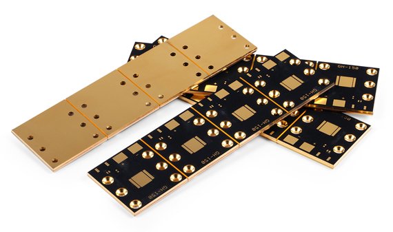
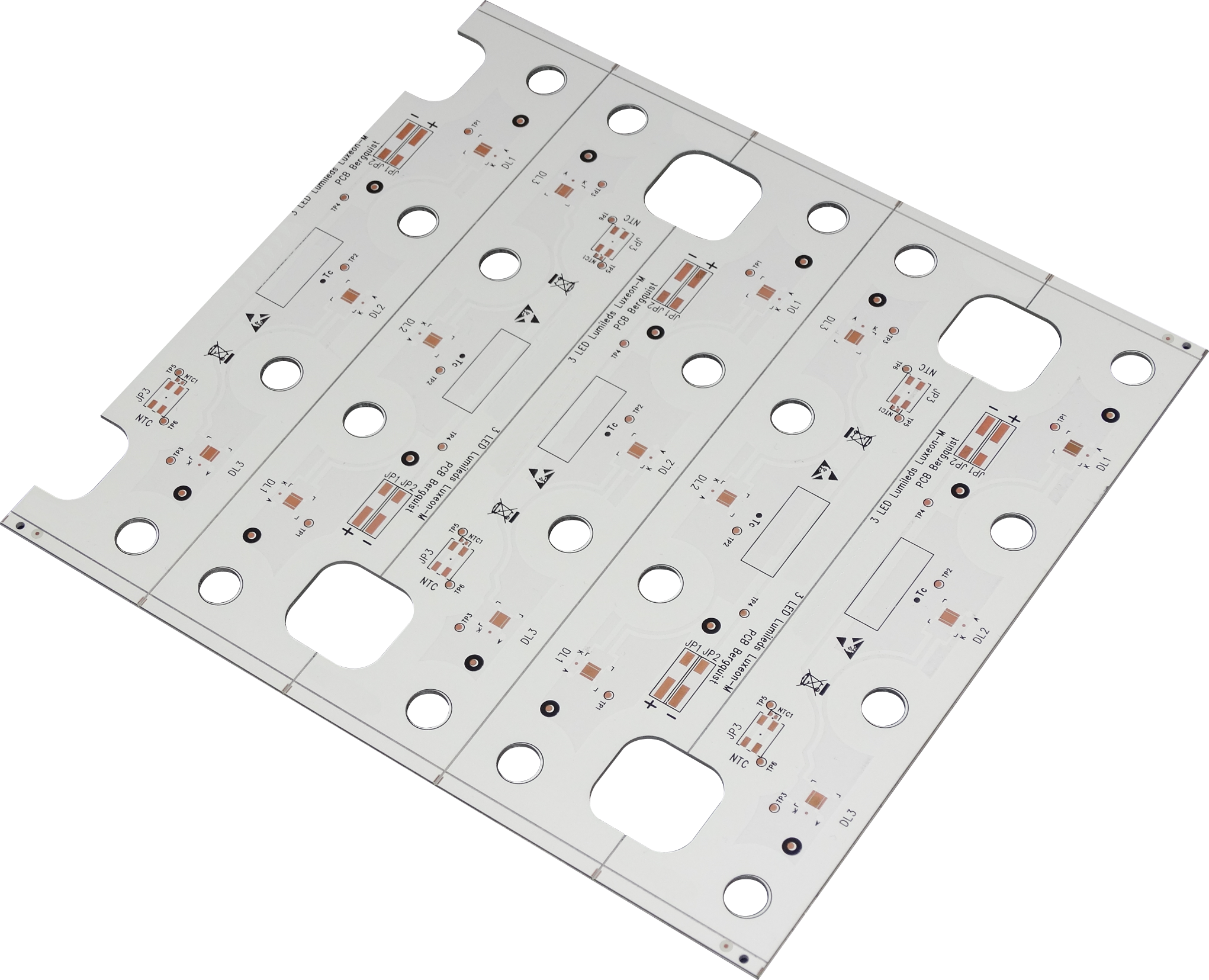
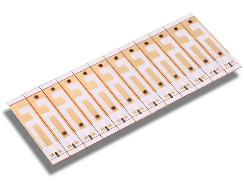
China stands as the global hub for PCB manufacturing, accounting for over 56% of the worldâs total output and leading innovations in high-layer boards, HDI technology, and automotive electronics PCBs. For businesses seeking reliable partners, understanding the China top 10 PCB manufacturers is critical to unlocking quality, efficiency, and technical expertise. These leading China PCB manufacturing company entities dominate key segments from AI server PCB China to new energy vehicles, with capabilities ranging from China PCB prototyping service to mass production. Whether youâre sourcing for consumer electronics or industrial control systems, the China top 10 PCB manufacturersrepresent the gold standard, backed by advanced equipment and global supply chain integration.
Exclusive Tesla Cybertruck PCB supplier; IATF 16949 certified
Huizhou, Guangdong Province
Guanghe Technology (001389.SZ)
Data center PCBs, AI-specific PCBs
74% overseas revenue; top 2 net profit margin in A-share PCB
Dongguan, Guangdong & Thailand
Dongshan Precision (002384.SZ)
FPC flexible boards, automotive PCBs
Appleâs 2nd largest FPC supplier; Tesla core partner
Changzhou, Jiangsu Province
Pengding Holdings (002938.SZ)
FPC (28% global share), SLP carrier boards
95%+ mass production yield; Appleâs top FPC supplier
Shenzhen, Guangdong Province
Jingwang Electronics
Rigid boards, FPC, 5G high-frequency PCBs
7 global production bases; one-stop procurement
Dongguan, Guangdong & Jiangxi
JLCPCB (Jialichuang)
32-layer prototyping, 0.15mm aperture
48-hour China PCB prototyping service; EDA to SMT turnkey solutions
Shenzhen, Guangdong Province
Liefeng PCB
Military-grade 12+ layer boards, 0.0762mm line width
24-hour prototyping; 99.9% on-time delivery
Shenzhen, Guangdong Province
How to Choose a China PCB Manufacturing Company
Selecting the right partner requires aligning needs with strengths. For AI server PCB China projects, prioritize firms like Shengyi Electronics with high-frequency material capabilities. For complex designs, choose high-layer PCB manufacturers China such as Shenghong Technology (70-layer capacity). For rapid iterations, verify China PCB prototyping service lead times (e.g., JLCPCBâs 48-hour delivery). Always check certifications: IATF 16949 for automotive, ISO 13485 for medical.
Core Pain Points of China PCB Manufacturing Company Entities
Raw material cost pressure (copper, CCL) squeezing margins for high-layer PCB manufacturers China
Price wars in mid-low end segments, impacting profitability of small China PCB manufacturing company teams
Skilled technician shortage for advanced HDI PCB suppliers China processes (laser drilling, resin)
Environmental compliance costs for wastewater treatment and emission reduction
Supply chain disruptions delaying AI server PCB China component procurement
Logistics Partnerships: DHL/FedEx collaborations for domestic/international delivery
Emergency Plans: Backup production lines for high-layer PCB manufacturers China equipment failures
Real-Time Tracking: Order monitoring systems and dedicated account managers
Historical Data: 99.9% on-time rate (e.g., Liefeng PCB) for similar order sizes
Contract Terms: Late delivery penalties ensuring accountability
Common Problems & Solutions for China PCB Manufacturing Company (FAQ)
Problem: Signal loss in AI server PCB China and 5G applications.
Solution: Adopt self-produced high-frequency materials (Shengyiâs 80%+ self-sufficiency) and optimize layouts via EDA design.
Problem: Delays from raw material shortages for HDI PCB suppliers China.
Solution: Partner with multiple CCL suppliers and maintain safety stock for critical components.
Problem: Low yield in high-layer PCB manufacturers China production.
Solution: Invest in laser drilling, 100% AOI inspection, and precision control training (Pengdingâs 95%+ yield model).
Problem: High cost of small-batch China PCB prototyping service.
Solution: Use intelligent panelization (JLCPCBâs optimization) to reduce waste and offer flexible pricing.
Problem: Inconsistent quality across China PCB manufacturing company batches.
Solution: Implement IoT-enabled real-time monitoring and standardized shift procedures.
Core Summary
Understanding the China top 10 PCB manufacturers provides curated high-quality partners, and leveraging selection criteria, capacity evaluation, and problem-solving ensures successful collaboration with the China top 10 PCB manufacturersâwhether sourcing AI server PCB China, high-layer PCB manufacturers China, or China PCB prototyping service solutions.
Hyderabad, a tech hub in Telangana, hosts a robust ecosystem of PCB manufacturing companies specializing in rigid, flexible, and multilayer boards for automotive, aerospace, and electronics sectors. For businesses seeking reliable partners, the Hyderabad top 10 PCB manufacturers stand out for their adherence to global standards (ISO, RoHS, UL) and tailored solutionsâfrom prototypes to high-volume production. Whether you need ceramic PCBs for industrial machinery or quick-turnaround assembly, the Hyderabad top 10 PCB manufacturers combine advanced technology (AOI testing, impedance control) and local expertise to meet diverse project needs, making the city a go-to destination for quality electronic components.
Cost-competitive bulk production, timely delivery, small business support
IDA Pashamylaram, Hyderabad
Precision Electronics Pvt. Ltd.
Solar panel PCBs, power transmitter modules, solid-state relay boards
Ceramic material specialization (AlN, Al2O3), high-temperature resistance, ISO 9001 certified
HITEC City, Hyderabad
How to Choose a Hyderabad PCB Manufacturer
Selecting the right PCB manufacturing company Hyderabad requires aligning your projectâs unique needs with a partnerâs strengths. Start by verifying industry expertiseâprioritize Hyderabad PCB suppliers with experience in your sector (e.g., automotive for Argus Systems, aerospace for Arks Microelectronics). Evaluate quality certifications (ISO 9001, IATF 16949) and compliance with RoHS/UL standards to ensure reliability. Assess manufacturing capabilities: confirm they handle your required layer count (up to 60 layers for complex designs) for multilayer PCB fabrication Hyderabad, material type (ceramic, FR4), and processes (blind vias, impedance control). Review turnaround time and minimum order quantityâsome manufacturers excel at rapid prototyping PCB Hyderabad (EmSys Argus) while others specialize in high-volume production (Argus Systems). Finally, check customer support: transparent communication, design feedback (DFM analysis), and post-delivery services (reworks, testing) are critical for long-term partnerships.
Core Pain Points of Hyderabad PCB Manufacturers
Raw Material Supply Chain Volatility: Fluctuations in availability of high-grade FR4, ceramic substrates, and copper foil disrupt production timelines, especially for multilayer PCB fabrication Hyderabad.
Skilled Labor Shortage: Gap in trained professionals for precision processes (e.g., blind via drilling, BGA assembly) leading to longer setup times and quality inconsistencies for automotive PCB manufacturers Hyderabad.
Cost Pressures from Global Competition: Balancing competitive pricing with investments in advanced equipment (AOI/X-ray machines) for Hyderabad PCB suppliers.
Lead Time Uncertainty for Custom Designs: Complex multilayer PCBs or low-volume rapid prototyping PCB Hyderabad face delays due to limited in-house tooling.
Quality Control Challenges for Miniaturized Components: Assembling 02001-sized SMT components requires ultra-precise equipment, leading to higher defect rates without regular calibration.
Regulatory Compliance Burden: Adapting to frequent updates in RoHS, REACH, and automotive (IATF 16949) standards increases costs for PCB manufacturing company Hyderabad.
Infrastructure Limitations: Power fluctuations and inconsistent logistics impact production stability for Hyderabad top 10 PCB manufacturers.
How to Evaluate Hyderabad PCB Manufacturer Production Capacity
Annual Production Volume: Verify maximum output (e.g., 1,000,000 units/year for Argus Systems) to ensure automotive PCB manufacturers Hyderabad handle your order size.
Equipment Sophistication: Check for automated lines (SMT assembly), AOI/X-ray inspection, and specialized machinery for multilayer PCB fabrication Hyderabad.
Layer Count & Material Expertise: Confirm capability to produce 1â60 layers and materials like ceramic for Hyderabad PCB suppliers.
Process Certification: Validate adherence to IPC-A-600 and IPC-610 standards for PCB manufacturing company Hyderabad.
Batch Flexibility: Assess ability to handle both rapid prototyping PCB Hyderabad (1-piece MOQ) and bulk runs.
Testing Capabilities: Ensure in-house testing (flying probe, thermal shock) to eliminate post-delivery failures for Hyderabad top 10 PCB manufacturers.
Scalability: Evaluate if Hyderabad PCB suppliers can ramp up production for sudden order increases.
How to Evaluate Hyderabad PCB Manufacturer Lead Time
Standard Turnaround Time (TAT): Request TAT for rapid prototyping PCB Hyderabad (3â7 days) vs. bulk (2â4 weeks) from PCB manufacturing company Hyderabad.
Urgent Order Handling: Inquire about hot-lot services for automotive PCB manufacturers Hyderabad and associated fees.
Supply Chain Transparency: Ask for sourcing timelines to identify bottlenecks for multilayer PCB fabrication Hyderabad.
Production Scheduling Efficiency: Assess if Hyderabad PCB suppliers use ERP systems to track orders.
Geographic Proximity to Suppliers: Hyderabad top 10 PCB manufacturers with local suppliers have shorter lead times.
Rework & Delay Contingencies: Confirm policies for delays with PCB manufacturing company Hyderabad.
Order Size Impact: Verify TAT consistency for rapid prototyping PCB Hyderabad and bulk orders.
Common Issues & Solutions for Hyderabad PCB Manufacturers (FAQ)
Issue: Delamination in PCBs during thermal stress for automotive PCB manufacturers Hyderabad. Solution: Use high-Tg substrates (â„170°C), optimize lamination parameters, and conduct pre-production testing.
Issue: Impedance mismatch in multilayer PCB fabrication Hyderabad. Solution: Partner with Hyderabad PCB suppliers offering ±10% tolerance via TDR testing and DFM reviews.
Issue: Solder mask peeling on PCBs from PCB manufacturing company Hyderabad. Solution: Ensure pre-treatment (cleaning), use UV-curable inks, and implement post-cure inspection.
Issue: Long lead times for multilayer PCB fabrication Hyderabad (10+ layers). Solution: Select Hyderabad top 10 PCB manufacturers with in-house tooling and pre-book production slots.
Issue: Quality inconsistencies between prototype and bulk for rapid prototyping PCB Hyderabad. Solution: Demand FAI for bulk runs and choose ISO 9001-certified Hyderabad PCB suppliers.
Issue: Non-compliance with RoHS for automotive PCB manufacturers Hyderabad. Solution: Verify lead-free processes (HASL, ENIG) and request certificates from PCB manufacturing company Hyderabad.
Issue: Poor communication with Hyderabad top 10 PCB manufacturers. Solution: Prioritize suppliers with dedicated account managers and real-time order portals.
This guide highlights the Hyderabad top 10 PCB manufacturers as trusted PCB manufacturing company Hyderabad partners, offering multilayer PCB fabrication Hyderabad, rapid prototyping PCB Hyderabad, and specialized solutions from automotive PCB manufacturers Hyderabadâreinforcing why the Hyderabad top 10 PCB manufacturers are the ideal choice for businesses seeking reliable Hyderabad PCB suppliers.
Taiwanâs PCB industry stands as a global leader, driven by advancements in AI, automotive electronics, and 5G communications, with a projected 5.7% growth in 2025 to reach NT$854.1 billion in production value. When it comes to Taiwan top 10 PCB manufacturers, these companies represent the pinnacle of technical expertise, manufacturing precision, and supply chain reliability, catering to global clients across consumer electronics, automotive, and semiconductor sectors. Whether youâre seeking high-density interconnect (HDI) boards, flexible PCBs, or advanced IC substrates, Taiwan top 10 PCB manufacturers deliver solutions that balance quality, innovation, and scalabilityâmaking them the go-to choice for businesses aiming to elevate their electronic products.
Top 10 PCB Manufacturers in Taiwan
Company Name
Process Capabilities
Core Advantages
Address
Unimicron Technology
HDI PCBs, IC substrates, rigid/flexible PCBs, packaging substrates
Global leader in advanced packaging, ISO/UL certified, key supplier to top electronics brands
No. 111, Jiankang Rd., Zhongli District, Taoyuan City 320, Taiwan
Precision manufacturing for miniaturized devices, ISO 13485 certification for medical applications
Taoyuan City, Taiwan
Chin-Poon Industrial
Multilayer PCBs, power electronics PCBs, renewable energy PCBs
High-temperature resistance technology, sustainable production practices
Kaohsiung City, Taiwan
Career Technology
HDI PCBs, server PCBs, network equipment PCBs
Edge AI and high-performance computing (HPC) expertise, fast prototype development
Taichung City, Taiwan
Jam Indo PCBA
PCBA assembly, custom PCB fabrication, low-volume high-mix production
One-stop solution (PCB + assembly), responsive technical support
Taipei City, Taiwan
How to Choose a Taiwan PCB Manufacturer
Selecting the right Taiwan PCB manufacturer requires a holistic evaluation of technical, quality, and operational factors to align with your project needs:
Verify Certifications: Prioritize manufacturers with ISO 9001, UL, IPC, and industry-specific certifications (IATF 16949 for automotive, ISO 13485 for medical). Confirm RoHS and REACH compliance for global market access.
Assess Process Capabilities: Match their technical specs (minimum line width/line spacing, layer count, special processes like blind/buried vias or impedance control) to your product requirements. For high-end needs, check HDI or IC substrate production experience.
Evaluate Quality Control Systems: Inquire about IQC (incoming material inspection), IPQC (in-process control), and OQC (outgoing quality control) processes. Look for traceability systems and failure analysis capabilities.
Check Production Capacity: Review monthly output (e.g., CCL sheets, PCB panels) and current order saturation to ensure they can meet your volume demands.
Validate Delivery Performance: Request on-time delivery rate data and ask about rush options. Assess their supply chain stability (e.g., backup raw material suppliers).
Test Sample Quality: Order prototypes to evaluate dimensional accuracy, electrical performance, and reliability. Conduct small-batch trials to confirm consistency.
Review After-Sales Support: Ensure they offer DFM (Design for Manufacturability) advice, quick response to quality issues, and a clear warranty policy.
Consider Cost-Effectiveness: Compare total ownership cost (TCO) rather than just unit price, factoring in quality risks and delivery delays.
Core Pain Points of Taiwan PCB Manufacturers
From a professional manufacturing perspective, Taiwan PCB manufacturers face key challenges impacting operations and competitiveness:
Intense Price Competition: Mid-to-low-end markets (e.g., standard multilayer PCBs) face pressure from domestic and international competitors, leading to compressed profit margins.
High Production Costs: Higher labor, equipment, and raw material costs compared to regional rivals, affecting cost competitiveness in mass-market segments.
Dependence on Key Clients: Over-reliance on large customers (e.g., Apple supply chain) exposes manufacturers to demand fluctuations and reduced bargaining power.
Technology Iteration Pressure: Rapid advancements in AI, 5G, and automotive electronics require continuous R&D investment to keep up with HDI, IC substrate, and advanced packaging demands.
Supply Chain Disruptions: Global component shortages (e.g., copper, resin) and geopolitical tensions impact raw material availability and pricing.
Capacity Allocation Challenges: Balancing domestic high-end production with overseas expansion (Southeast Asia) to optimize costs while maintaining quality.
Talent Shortage: Gap in skilled labor for advanced manufacturing processes (e.g., laser drilling, automated inspection) affecting production efficiency.
How to Evaluate Taiwan PCB Manufacturersâ Production Capacity
Use these critical metrics to assess a manufacturerâs ability to deliver consistent, high-quality PCBs at scale:
Monthly Production Volume: Check output data (e.g., CCL sheets, PCB panels, or finished PCBs) to confirm alignment with your order size.
Equipment Sophistication: Verify advanced machinery such as LDI (laser direct imaging) systems, AOI (automatic optical inspection) tools, and CNC drilling machines.
Process Capability Metrics: Review minimum line width/line spacing (e.g., 3/3mil or 1/1mil for high-density needs), maximum layer count (12+ layers for complex products), and special process capabilities (HDI, blind/buried vias).
Quality Yield Rate: Ask for first-pass yield (FPY) dataâtop manufacturers maintain FPY above 98% for standard processes and 95% for complex PCBs.
R&D Investment: Evaluate R&D spending as a percentage of revenue and number of patents (especially in advanced materials or processes).
Production Line Flexibility: Assess ability to handle low-volume high-mix orders (prototypes) and high-volume mass production with quick changeover times.
Raw Material Sourcing Stability: Confirm long-term contracts with reliable suppliers and backup sourcing plans for critical materials (copper, FR4, solder mask).
Facility Expansion Plans: Review investments in new plants (domestic or overseas) to ensure capacity growth matches future demand.
Energy Efficiency: Modern, energy-saving facilities reduce production bottlenecks and operational costs.
How to Evaluate Taiwan PCB Manufacturersâ Lead Time
Accurate lead time assessment ensures your project timeline stays on trackâuse these factors to evaluate reliability:
Standard Lead Time for Your Product Type: Confirm typical turnaround for your PCB specs (e.g., 48 hours for 2-layer FR4, 7-10 days for 12-layer HDI).
Order Priority System: Inquire about rush options (e.g., 24-hour rush service) and associated fees.
Production Schedule Transparency: Ask if they provide real-time order tracking or regular updates on production progress.
Capacity Utilization Rate: Avoid manufacturers operating at 90%+ capacity, as this increases risk of delays.
Supply Chain Lead Time: Assess raw material procurement timelines (e.g., 3-5 days for standard materials vs. 2+ weeks for specialty substrates).
Quality Control Time: Ensure QC processes (e.g., flying probe testing, X-ray inspection) are integrated without excessive delays.
Logistics Partnerships: Check if they have established relationships with reliable couriers (e.g., DHL, FedEx) for timely shipping.
Historical On-Time Delivery Rate: Request data from the past 6-12 monthsâtarget manufacturers with 95%+ on-time performance.
Contingency Plans: Ask how they handle production disruptions (e.g., equipment breakdowns, material shortages) to minimize delays.
Communication Responsiveness: Quick responses to lead time inquiries indicate efficient customer service and operational transparency.
Common Issues of Taiwan PCB Manufacturers (FAQs & Solutions)
Q1: What causes alignment inaccuracies in multilayer PCBs, and how is it resolved?
A: Misalignment often stems from outdated positioning equipment or material warpage. Taiwan manufacturers use high-precision optical alignment systems and automatic correction technology to achieve micron-level alignment, paired with strict material pre-treatment (e.g., humidity control) to prevent warpage.
Q2: How to address poor solderability on PCB surfaces?
A: Solderability issues result from inconsistent plating thickness or oxidation. Solutions include optimizing plating bath composition, controlling temperature/stirring during surface treatment, and using OSP (Organic Solderability Preservative) or lead-free tin spraying processes with post-treatment oxidation protection.
Q3: What leads to signal integrity problems in high-frequency PCBs, and how to fix them?
A: Signal degradation is caused by improper impedance control or layout design. Manufacturers use impedance simulation tools during design, select low-loss materials (e.g., high-frequency FR4), and optimize trace routing to minimize crosstalk.
Q4: How to resolve delayed deliveries due to raw material shortages?
A: Shortages of copper or resin are mitigated by maintaining strategic raw material stockpiles, partnering with multiple global suppliers, and prioritizing long-term contracts to secure supply.
Q5: What causes hole wall roughness in drilled PCBs, and how is it improved?
A: Rough hole walls result from dull drill bits or incorrect drilling parameters. Manufacturers regularly calibrate and replace drill bits, adjust speed/feed rates based on board material characteristics, and use high-pressure water cleaning post-drilling.
Q6: How to handle quality inconsistencies in mass production?
A: Inconsistencies arise from inadequate process control. Solutions include implementing real-time IPQC (in-process quality checks), automated inspection systems (AOI/X-ray), and batch traceability to identify and resolve bottlenecks.
Q7: What to do if the PCB fails thermal stress testing for automotive applications?
A: Thermal failure is addressed by using high-temperature resistant materials (e.g., polyimide), optimizing copper pour for heat dissipation, and integrating thermal vias or heat sinks into the design.
Q8: How to resolve cost overruns for custom PCB orders?
A: Overruns occur from design inefficiencies or material waste. Manufacturers provide DFM (Design for Manufacturability) advice to simplify complex features, optimize panel utilization to reduce waste, and offer transparent cost breakdowns upfront.
This guide highlights Taiwan top 10 PCB manufacturers as global leaders in quality and innovation, while providing actionable insights to select, evaluate, and collaborate effectively with these providersâproving that Taiwan top 10 PCB manufacturers remain the preferred choice for businesses seeking reliable, high-performance PCB solutions in todayâs competitive electronics industry.
How to design RF power supply PCB for reliability? This blog is mainly about material selection, impedance control, thermal management, and EMI suppression for RF PSU PCB design.
Are you troubled these problems with RF power supply PCB?
Does your RF power supply PCB suffer from unstable output power and efficiency degradation due to high-frequency signal crosstalk?
Are thermal management challenges in high-speed RF modules causing overheating risks and performance decay?
Do long lead times and uncontrolled costs during small-batch trial production delay your market entry opportunities?
As a RF power supply PCB manufacturer, Best Technology can provide you service and solutions:
High-Frequency Signal Optimization: Full-chain simulation from stack-up design to impedance matching ensures signal integrity and stable power output.
Intelligent Thermal Management: Advanced thermal conductive materials and optimized layout design reduce heat buildup, extending module lifespan by 30%.
Agile Supply Chain Support: Rapid prototyping with 7-day sample delivery and flexible production scaling achieves 15-day mass production readiness, accelerating time-to-market while controlling costs.
Prioritize low-loss dielectric materials: For high-frequency environments, select substrates with stable dielectric constant (Dk) and low loss tangent (Df), such as PTFE or hydrocarbon resin-based materials. This minimizes signal attenuation and thermal losses, ensuring efficient power conversion.
Ensure thermal-mechanical compatibility: Match the coefficient of thermal expansion (CTE) of the material with copper foil and chip packaging materials. This prevents delamination, cracks, or long-term reliability degradation caused by thermal stress during high-temperature soldering or power cycling.
Enhance environmental resilience: For high-humidity, high-temperature, or corrosive environments, use moisture-resistant and chemically inert coating materials (e.g., modified rosin resins) or surface treatments. This prevents dielectric absorption, copper migration, or insulation failure.
Balance cost and performance: Select materials based on power levels and application scenarios. High-frequency, high-power designs may require premium low-loss substrates, while mid/low-frequency applications can leverage cost-effective FR-4 variants. Validate reliability through multi-physics simulations (thermal-electrical-mechanical coupling).
Verify manufacturing process compatibility: Confirm materials align with existing PCB fabrication processes (e.g., lamination temperatures, drilling parameters, surface finishes). Avoid issues like inner-layer voids, pad lifting, or impedance variations that compromise yield and long-term reliability.
Impedance Control in RF Power Supply PCB Design
Core Goal of Impedance Matching: Ensure signal path impedance aligns with source and load impedance to minimize signal reflection and power loss. In high-frequency scenarios, minor impedance deviations can cause signal distortion or reduced power transmission efficiency, requiring strict control within design tolerances.
Critical Parameter Control: Maintain characteristic impedance at 50 ohms or 75 ohms (per system standards) with a typical error margin of ±10%. Focus on geometric dimensions of transmission lines (e.g., microstrip lines, striplines, coplanar waveguides), including trace width, spacing, dielectric thickness, and dielectric constant.
Material Selection and Stack-Up Design: Prioritize low-loss substrates (e.g., Rogers series or high-frequency FR-4 variants) for stable dielectric constants. Balance signal, power, and ground layers in stack-up design to avoid inter-layer crosstalk. Multi-layer boards require clear inter-layer impedance coupling relationships and optimized inter-layer dielectric thickness.
Layout and Routing Guidelines: Keep high-frequency signal traces short, straight, and minimize bends/vias. Isolate sensitive lines (e.g., power amplifier outputs) from digital signals to prevent cross-interference. Power paths should account for current capacity and voltage drop, using wide copper traces or parallel routing to reduce impedance.
Grounding and Shielding Strategies: A continuous ground plane forms the foundation of impedance control; avoid splitting ground planes to prevent impedance discontinuities. Use localized shielding cans or ground via arrays in critical circuit areas to reduce electromagnetic radiation and external interference.
Power Integrity Management: Control impedance fluctuations in the power distribution network using decoupling capacitor networks to suppress high-frequency noise. Place capacitors near power-consuming components to create low-impedance return paths and stabilize supply voltage.
Thermal Management and Material Durability: Account for impedance variations with temperature in high-power RF circuits by selecting high-temperature-resistant substrates and surface finishes. Coordinate thermal design with impedance control to prevent dielectric deformation or impedance drift due to thermal stress.
RF Power Supply PCB Layout Optimization for Signal Integrity
1. Physical Partitioning and Electrical Isolation
Zone Division
Strictly separate RF, digital, and power zones using “I-shaped” or “L-shaped” layouts to minimize signal path crossings.
Avoid U-shaped signal paths to prevent self-interference.
Component Placement
Isolate high-power amplifiers (PA) and low-noise amplifiers (LNA) by â„1.5cm, placing them on opposite PCB sides to reduce thermal coupling.
Dedicate shielded cavities for sensitive analog circuits (e.g., VCOs) with non-square aspect ratios to suppress resonance.
2. Impedance Matching and Transmission Line Design
Use 45° curved routing to reduce reflections; trace width â„15mil (high-frequency scenarios), spacing â„2W (W=1/10 signal wavelength).
Differential Pair Design
Symmetrically route differential pairs with adjacent ground traces and via stitching; avoid parallel routing to prevent crosstalk.
Limit via count in critical paths (e.g., antenna feedlines) to â€3 per 10cm; backdrilled stub length â€50ÎŒm.
3. Ground System Optimization
Ground Plane Integrity
Employ continuous multi-layer ground planes (e.g., layer 2 as GND) without islanding or cuts.
For frequencies >1GHz, implement multi-point grounding with signal return paths tightly adjacent to signal traces.
Via Placement
Place ground vias every 1-2mm alongside key RF paths to form “fences”; match via placement for differential signals.
Shield cans must connect to the ground plane at â„3 points; aperture size â€Î»/10 to prevent high-frequency leakage.
4. Decoupling Capacitor Hierarchy
Tiered Decoupling System
Chip-Level: 0402 1nF MLCC placed â€1mm from BGA pins for high-frequency noise suppression.
Module-Level: 0603 10nF+100nF combination for 100MHz-1GHz band; ensures low-impedance path.
System-Level: 3216 4.7ÎŒF tantalum capacitor to mitigate low-frequency power ripple.
Grounding Consistency
Ensure capacitor ground terminals share a common ground via direct connection to the ground plane; avoid series vias that cause ground potential inconsistencies.
5. EMC and Shielding Design
High-Power Region Isolation
Reserve intact ground planes under high-power regions without vias to maintain signal integrity.
Achieve â„30dB isolation between RF output and input; add shielding if necessary.
Sensitive Signal Protection
Shield sensitive signals (e.g., clock lines) using stripline routing with â„10mil width, flanked by ground traces and vias.
For digital/analog crossings, use layered routing with intermediate ground planes to prevent capacitive coupling.
6. Thermal Management
Heat Distribution
Distribute heat evenly across the PCB to avoid local hotspots; use â„2oz copper thickness under high-power devices.
Connect high-power components to heatsinks using thermal adhesive/pads; use metallized mounting holes (â„3mm diameter) under PAs for enhanced heat dissipation.
Thermal Validation
Validate thermal distribution via tools like Ansys to ensure temperature rise â€40°C; consider thermal expansion coefficient matching.
7. Verification and Simulation Tools
Impedance Validation
Verify impedance using SI9000 and TDR with ±5% tolerance; confirm resonance points via VNA frequency response testing (0.1-10GHz).
Reliability Testing
Conduct thermal cycling tests (-55°C to 125°C) to validate long-term reliability; use Ansys HFSS/CST for electromagnetic field analysis to optimize shield can dimensions and via placement, ensuring first-pass EMC compliance.
Heat Dissipation Strategies for 100W RF Power Supply PCBs Design
1. High-Thermal-Conductivity Substrate Selection
Metal Substrate Application: Replace traditional FR4 with aluminum substrate (thermal conductivity 2â5 W/m·K) or copper substrate (385 W/m·K) for high-heat devices like RF power amplifiers (RF PA) and MOSFETs. For example, aluminum substrates can reduce 100W MOSFET temperature from 95°C to 65°C, significantly enhancing reliability.
Ceramic Substrate Solution: Aluminum nitride (AlN) or silicon carbide (SiC) ceramic substrates offer thermal conductivity of 170â200 W/m·K, suitable for high-frequency high-power scenarios such as 5G RF modules, preventing interlayer cracking due to mismatched thermal expansion coefficients.
Thick Copper Foil Process: Use 4oz (140ÎŒm) or 6oz (210ÎŒm) copper foil with large-area power/ground copper foil design, achieving heat dissipation capacity exceeding 0.8W/cmÂČ to meet 100W power requirements.
2. Thermal Flow Path Optimization Layout
Device Zoning Strategy: Place high-heat devices (e.g., RF PA, DC-DC modules) at PCB edges or upper layers to shorten heat conduction paths. Position sensitive components (e.g., small-signal transistors, crystals) in cool air inlets, avoiding direct placement above heat sources.
Thermal Via Array Design: Deploy dense 0.3mm-diameter thermal vias (spacing â€0.6mm) beneath power devices to create low-thermal-resistance channels to bottom-layer heat sinks. For instance, 100W RF PA with 100 vias/cmÂČ can lower temperature by 15°C.
Airflow Management: Design airflow paths to avoid component obstruction, combining horizontal/vertical heat sinks with forced air cooling (fans) or natural convection to optimize airflow and ensure efficient hot air exhaust.
3. Active and Passive Heat Dissipation Synergy
Heat Sink Selection: Aluminum fin heat sinks (fin height 10â20mm) suit 10â100W scenarios; above 100W, recommend water-cooled heat sinks or heat pipe systems (e.g., rocket-grade heat pipes) using phase-change principles for efficient heat transfer.
Interface Material Application: Use thermal grease (3â5 W/m·K) or thermal silicone pads (2â4 W/m·K) to fill gaps between devices and heat sinks, reducing thermal resistance below 0.1°C/W and preventing thermal failure from air gaps.
Liquid Cooling Integration: Embed microchannel liquid cooling structures in PCBs or adopt integrated coolant nozzles directly contacting high-heat device bases, enabling efficient heat dissipation via fluid circulation for enclosed chassis or high-density installations.
4. Thermal Simulation and Testing Verification
Simulation Tool Application: Utilize software like ANSYS Icepak or FloTHERM for thermal simulation, identifying hotspots and optimizing copper foil layout, via density, and heat sink shapes. For example, adjusting via diameter and spacing via simulation can reduce thermal resistance by over 30%.
Experimental Testing Methods: Monitor PCB surface temperature distribution with thermal imagers and collect real-time data via temperature sensors to validate heat dissipation design. Critical points (e.g., power device solder joints) require thermal cycling tests to ensure long-term reliability.
Material Thermal Characteristic Verification: Test thermal expansion coefficients and conductivity of substrates (e.g., Rogers 4350B, aluminum substrates) to ensure compatibility with device parameters, preventing interlayer separation or solder joint failure due to thermal stress.
5. Process and Structural Innovation
Mesh Copper Foil Design: Design large-area copper foil as mesh (minimum grid 0.025-inch) without compromising electrical performance, reducing soldering thermal stress and preventing copper foil blistering or board warping.
Thermal Isolation Rings and Heat Dissipation Strips: For large pads or high-current traces, use thermal isolation rings to minimize soldering heat conduction impact on adjacent areas. Heat dissipation strip width should match pad diameter (typically 60% of pad diameter) to ensure concentrated heat export.
Modular Heat Dissipation Solutions: Adopt standardized heat dissipation modules (e.g., fin heat sinks, heat pipe assemblies) with plug-and-play designs for easy maintenance and upgrades, while reducing overall system thermal resistance.
Best Practice for Grounding the Shield Can on an RF PSU PCB
Shortest Return Path: Critical RF signals (e.g., antenna feedlines, PA outputs) require “via fence” technologyâdense grounding vias spaced every 1-2mm (â€Î»/10) along signal paths, forming a Faraday shielding cage to suppress dipole antenna effects.
Grounding Strategy Selection: High-frequency circuits (>100MHz) mandate multi-point grounding via dense vias (4-6 per cmÂČ) connecting ground planes. Low-frequency circuits (<100MHz) may use single-point grounding to avoid ground loop noise.
2. Physical Grounding Specifications for Shield Cans
Material & Contact Design: Shield cans prioritize tin-plated steel, copper, or aluminum with soldered or spring-loaded clip fastening. Solder pads must be â„0.5mm wide, spaced â€2mm, using high-conductivity solder (e.g., SnAgCu) or conductive adhesive for low-impedance contact. Removable shields require 360° contact via spring clips or conductive foam to prevent floating ground-induced shielding failure.
Opening & Ventilation Control: Aperture size strictly limited to â€Î»/10 (e.g., 1.25cm for 2.4GHz signals). Ventilation holes must use honeycomb structures or metal mesh to prevent RF leakage.
Edge Grounding Enhancement: PCB edges adopt metallized edge wrapping (copper width â„2mm) or ground rings combined with spring-clip grounding to ensure low-impedance connections between shields and PCB edges, reducing parasitic resonance risks.
3. PCB Stackup & Structural Optimization
Recommended Layer Stackup: Standard 4-layer configuration: Top layer (RF signal layer), Layer 2 (ground plane), Layer 3 (power layer), Bottom layer (signal layer). 2-layer boards must designate the bottom layer as a full ground plane, reserving the top layer for critical RF traces.
Via & Grounding Network: Double-row via arrays spaced â€1mm surround critical RF regions (e.g., LNA/PA modules) to form low-impedance return paths. Blind/buried vias suit high-density HDI boards, reducing via parasitic inductance.
Case Study Evidence: 5G mmWave modules reduced EMI leakage by 20dB and crosstalk by 30% by shrinking ground pad spacing to 1.5mm, adding dual via rows (1mm spacing), and implementing spring-clip edge grounding. Wi-Fi modules restored receiver sensitivity and reduced error rates to <10â»â¶ via local grid copper flood (â€Î»/2 spacing) and via density up to 5/cmÂČ.
Simulation & Measurement Synergy: Design phase uses Ansys HFSS/CST Microwave Studio for ground impedance and S-parameter simulation (target Sââ<-10dB, Sââ<-30dB). Measurement phase employs near-field probes and spectrum analyzers to validate shielding effectiveness per ETSI/FCC standards.
Regulatory Compliance: Adheres to Radio Equipment Directive 2014/53/EU. Cable shields require 360° bonding to connector shells, avoiding “pig-tail” wiring to minimize inductance-induced high-frequency noise.
5. Special Scenarios & Key Considerations
High-Speed SerDes Interfaces: Adopt coplanar waveguide (CPW) structures to ensure tight signal-ground coupling and reduce radiation loss.
mmWave Band Challenges: >30GHz bands require exploration of 3D metallization packaging or nano-conductive materials, as conventional vias may fail. AI-driven simulation optimizes shielding structures.
ESD Protection: Chassis ground connects to system ground via low-impedance paths, paired with TVS diodes to suppress transient disturbances, ensuring human safety and system stability.
RF Power Board Harmonic and EMI Suppression Solutions
 1. Harmonic Suppression Core Strategies
Use LC filter banks (e.g., Ï-type/T-type structures) to precisely suppress specific frequency harmonics. Recommend inductors with high saturation current and low core loss using ferrite material, and capacitors with X7R/X8R ceramic for balanced temperature stability and cost.
For switching power modules, connect common-mode chokes + Y-capacitors in parallel at input/output terminals to suppress common-mode noise in 150kHz-30MHz range. Add series differential-mode inductors to filter differential-mode interference, ensuring compliance with CISPR 22 Class B standards.
2. EMI Source Control and PCB Layout Optimization
High-frequency signal paths follow “short, direct, wide” principles: critical RF traces (e.g., PA output) should be †λ/10 in length to avoid antenna effects; use â„20mil copper thickness to reduce current density and parasitic inductance.
Sensitive components (e.g., LDOs, crystals) should be isolated from high-frequency areas using “thermal island” designs, with through-hole arrays for shielding to reduce crosstalk.
3. Shielding and Material Selection Practices
Metal shielding cans use 1-2mm thick aluminum-magnesium alloy with nickel plating for oxidation resistance. Install conductive foam at openings for 360° grounding. For cavity resonance frequencies, apply absorber coatings (e.g., ferrite layers) to suppress standing waves.
PCB substrates prioritize low-loss high-frequency materials like RO4350B/RO4003 (dielectric constant 3.48±0.05) with ENIG surface finish for solder reliability and reduced surface roughness impact on signal integrity.
4. Grounding System Design Standards
Single-point grounding suits low-frequency scenarios (<1MHz); high-frequency modules adopt multi-point grounding connected to the bottom-layer ground plane to form low-impedance networks. For mixed-signal systems, recommend “star” grounding topology with the center point connected to chassis ground via low-impedance paths.
Ground vias should be spaced 5-8mm apart to avoid ground loops. Critical interfaces (e.g., SMA, I/O) use ground springs for direct connection to metal enclosures, ensuring continuous low-impedance grounding paths.
5. Test Verification and Standards Alignment
Pre-certification stages use near-field probes to scan PCB areas, locate over-limit frequencies (e.g., 100MHz, 300MHz), and optimize layouts or add filter capacitors. Formal testing requires 3m anechoic chamber radiation scans to meet FCC Part 15, EN 55032, and other international standards.
Recommend real-time debugging with spectrum analyzers + near-field probes, complemented by EMI receivers for full-band scans. For harmonic issues, use oscilloscopes to observe power waveform distortions and supplement with harmonic compensation circuits (e.g., PFC circuits) to optimize power factors.
RF Power Supply PCB Design Verification Methodologies
1. Signal Integrity Verification
Use Time-Domain Reflectometry (TDR) and Eye Diagram Analysis to verify high-speed signal integrity, ensuring no impedance discontinuity or reflection in RF signal transmission paths.
Perform differential pair line width/spacing tolerance analysis, simulate signal loss under different process variations using tools like ADS/HFSS, and ensure design margin â„20%.
Conduct crosstalk simulation for critical signals (e.g., control lines, clock lines), with adjacent signal spacing adhering to the 3W rule (â„3Ă line width).
2. Power Integrity Verification
Conduct DC Drop analysis on power planes to ensure voltage drop â€2%, preventing localized voltage deficiency-induced device performance degradation.
Analyze power noise coupling using power integrity tools (e.g., Sigrity), and design decoupling capacitor networks for high-frequency noise, with capacitance values matched to target impedance via Z-parameters.
Implement dynamic voltage fluctuation testing, measure power ripple under actual operating conditions with an oscilloscope, and ensure â€1% peak-to-peak value.
3. Thermal Management Verification
Perform thermal distribution analysis using thermal simulation tools (e.g., FloTHERM), with junction temperatures of critical power devices (e.g., MOSFETs, LDOs) below 85°C safety threshold and 15% thermal design margin reserved.
Design thermal paths including thermal pads/copper blocks, via arrays, and thermal pads, ensuring thermal resistance â€10°C/W.
Execute temperature cycling tests (-40°C to 125°C) to validate solder joint reliability and material CTE (Coefficient of Thermal Expansion) matching.
4. EMC/EMI Compliance Verification
Conduct radiated emission pre-scans using near-field probes and spectrum analyzers, focusing on switching power noise, RF harmonics, and ground loop issues.
Design low-impedance grounding networks with star-point grounding topology to avoid ground bounce noise, with ground plane coverage â„80% of PCB area.
Perform conducted emission testing (e.g., EN55022 standard), suppress high-frequency noise via filter capacitor/inductor combinations, and ensure conducted interference â€40dBÎŒV (30MHzâ1GHz).
5. Manufacturability & Reliability Verification
Execute Design Rule Checks (DRC) to ensure line width/spacing and via dimensions comply with fabricator capabilities (e.g., minimum 4mil line width, 8mil via diameter).
Validate pad design compatibility (e.g., HASL/ENIG surface finishes) and BGA device pad symmetry.
Conduct reliability acceleration tests (e.g., HAST, TC) to verify solder joint mechanical strength and material moisture/thermal resistance, ensuring MTBF â„100,000 hours.
6. RF Performance Special Verification
Measure RF power amplifier input/output impedance using network analyzers, tune matching networks via Smith charts, and ensure S11 †-15dB (return loss).
Implement power efficiency testing, measure PAE (Power-Added Efficiency) using power meters and DC supplies, with target â„60% at operating frequency.
Adopt EDA toolchains (e.g., Altium/Cadence) for schematic-PCB-simulation collaborative verification, ensuring real-time synchronization of design changes.
Implement design review mechanisms with independent teams cross-verifying signal path integrity, PDN (Power Distribution Network) noise, and thermal design rationality.
Establish a verification issue tracking system to classify discovered issues (Critical/Major/Minor) and formulate remediation plans, ensuring closed-loop management.
A â2+N+2 stackupâ is a specific high-density interconnect (HDI) printed circuit board configuration, characterized by two sequential lamination cycles building up HDI layers on either side of a core. This architecture is fundamental for creating the dense, reliable, and high-performance interconnections required in modern electronics. This article will explore the structure, benefits, and design considerations of the 2+N+2 stackup, explaining why it is often the ideal choice for complex HDI PCB manufacturing.
Are you struggling to pack more functionality into a smaller PCB footprint while maintaining signal integrity and reliability? As devices shrink and performance demands soar, standard PCB constructions often hit a wall. Designers frequently encounter:
âSignal Integrity Issues:ââ Increased crosstalk and impedance discontinuities in complex, dense layouts.
âLimited Routing Density:ââ Inability to escape from fine-pitch BGAs and other advanced components with standard through-hole vias.
âManufacturing Complexity and Cost:ââ Difficulty balancing the performance needs of HDI with a cost-effective and reliable fabrication process.
âReliability Concerns:ââ Weak points in the via structure, especially when connecting multiple layers, leading to potential failures.
âThermal Management Challenges:ââ Effectively dissipating heat in a compact, multi-layer board.
Fortunately, the â2+N+2 stackupâ directly addresses these challenges. This HDI approach provides a structured path to higher performance without compromising on manufacturability. The key solutions it offers include:
âSuperior Signal Integrity:ââ Controlled impedance and reduced crosstalk through well-defined microvia structures and optimized dielectric spacing.
Maximum Routing Density: Efficient component escape routing using stacked or staggered microvias, enabling HDI 1+n+1 and beyond.
âOptimized Manufacturing Flow:ââ A balanced structure that leverages proven sequential lamination cycles, improving yield and controlling costs.
âEnhanced Reliability:ââ Robust interconnects with stacked or staggered vias that are more reliable than complex through-hole via structures in thin boards.
âEffective Thermal and Power Distribution:ââ A dedicated core section (N) for solid power and ground planes, improving heat spreading and PDN stability.
At BEST Technology, we specialize in advanced PCB manufacturing, with deep expertise in HDI and complex stackups like 2+N+2. Our engineering support team can help you optimize your design for performance, reliability, and cost-effectiveness, ensuring your product succeeds in a competitive market. For inquiries, please contact us at âsales@bestpcbs.com.
What is 2+N+2 Stackup?
In essence, a 2+N+2 stackup describes the layer build-up of an HDI PCB. The notation breaks down as follows:
The first and last “â2â” represent two HDI layers built sequentially on the top and bottom of the board. These layers typically use microvias (laser-drilled) for interconnection.
The “âNâ” represents the internal core, which can be any even number of layers (e.g., 2, 4, 6). This core is manufactured separately and contains standard mechanically drilled plated through holes (PTHs). This structure requires two separate lamination cycles: first to create the core, and second to laminate the top and bottom HDI buildup layers onto it. This is a step beyond a simpler âHDI 1+n+1â stackup, offering greater routing density and design flexibility.
As shown in the photo below:
L1 build-up
L2 build-up
L3 core
L4 core
L5 build-up
L6 build-up
What is a Typical PCB Stackup?
A typical PCB stackup refers to the arrangement of copper and insulating layers that make up a circuit board. Its primary functions are to:
âProvide Shielding:ââ Ground planes are strategically placed to shield sensitive signals from noise.
âManage Heat and Power:ââ Dedicated planes distribute power and help dissipate heat.
A standard stackup might be simple, like a 2-layer board, or complex, like the â2 n 2 stackup HDIâ used for advanced applications. The choice depends entirely on the circuit’s complexity and performance requirements.
What is a 2 Layer PCB Structure?
A 2-layer PCB, the simplest multilayer structure, is defined by the following key characteristics:
âLayer Structure:ââ It is composed of three fundamental elements:
A top copper layer for components and traces.
A dielectric substrate core (e.g., FR-4) in the middle.
A bottom copper layer for components and traces.
âKey Features:ââ
Components and routing traces can be placed on both the top and bottom sides of the board.
Electrical connections between the two layers are made exclusively using plated through-hole (PTH) vias, which are holes drilled through the entire board and plated with copper.
What is the Standard 1.6 mm 2 Layer Stackup? A common standard for a 2-layer PCB is a 1.6mm overall thickness. A typical build-up might be:
Top Layer: 1 oz (35”m / 0.035mm) Copper
Dielectric Core: ~1.5mm (e.g., FR-4)
Bottom Layer: 1 oz (35”m / 0.035mm) Copper
This simple structure is cost-effective but offers limited routing space and cannot support the high-speed or dense designs that necessitate an âadvanced circuits stackupâ like 2+N+2.
What are the Standard HDI Stackups?
HDI stackups are classified by the number of sequential laminations and the via structures used. The most common standard HDI stackups are:
â1+N+1:ââ This is the simplest HDI type, featuring one HDI buildup layer on each side of the core. It primarily uses microvias to connect the surface layer directly to the first inner layer.
â2+N+2:ââ This stackup features two HDI buildup layers on each side of the core. This allows for more complex routing and a higher density of components. The microvias can be implemented in either a stacked or staggered configuration.
â3+N+3 and Beyond:ââ Used for extremely complex designs, these stackups require three or more sequential lamination cycles. They offer the highest possible density and component integration but at a significantly greater cost.
What is the Difference between Stacked and Staggered Via?
In a â2 n 2 stackup HDI PCB, microvias connecting different layers can be arranged in two primary ways:
âStacked Vias:ââ Microvias are placed directly on top of one another, creating a continuous vertical connection through multiple HDI layers. This saves horizontal space but can be more challenging to manufacture reliably due to potential voiding in the fill material.
âStaggered Vias:ââ Microvias are offset from one another, connecting adjacent layers in a step-like pattern. This is often more reliable from a manufacturing standpoint but consumes more routing area on the inner layers.
The choice between stacked vs. staggered depends on density requirements, manufacturer capability, and reliability specifications.
What is V in PCB Board?
In the context of vias, “V” simply stands for “Via.” A via is a plated hole that provides an electrical connection between different layers of a PCB. In HDI discussions, you’ll encounter terms like:
âMicrovia:ââ A small via (typically <0.15mm diameter) laser-drilled, used in HDI layers.
âThrough-Hole Via:ââ A via that passes through the entire board.
âBlind Via:ââ Connects an outer layer to an inner layer without going through the entire board.
âBuried Via:ââ Connects inner layers only and is not visible on the surface.
How Much Current can a 0.2 mm Trace Carry?
The current-carrying capacity (ampacity) of a PCB trace mainly depends on its cross-sectional area (trace width Ă copper thickness) and how well the board dissipates heat. External traces carry more current than internal traces because they cool more efficiently.
For a 0.2 mm (â8 mil) wide, 1 oz (â35 ”m) external copper trace on FR-4, a practical estimate for a 10°C temperature rise is around 1.0 A. Below is a simplified calculation using clear text (no formulas that will break when pasted).
1. Define the trace geometry
Trace width: 0.2 mm â 8 mil
Copper thickness (1 oz): 35 ”m â 1.37 mil
2. Calculate the cross-sectional area
Area = width (mil) Ă thickness (mil)
Area â 8 mil Ă 1.37 mil
Result â 11 milÂČ
3. Apply the IPC-2221 external-trace approximation
IPC-2221 uses an empirical relationship between:
current
trace area
temperature rise
Using the simplified IPC-2221 external-layer approximation:
At ÎT â 10°C
Area â 11 milÂČ
Copper thickness = 1 oz
The resulting ampacity is roughly 0.7â0.8 A.
4. Compare with IPC-2152 (newer standard)
IPC-2152 generally gives slightly higher allowable currents for the same conditions.
For a 0.2 mm (8 mil) external trace at 1 oz copper and 10°C rise:
IPC-2152 calculators usually give 0.8â1.0 A
⭐ Practical design value
To keep it simple and safe:
A 0.2 mm external trace with 1 oz copper can typically carry about 1 A for a small temperature rise.
✔ Design Recommendations
1. Always confirm with an IPC-2152-based trace-width calculator
This is essential for power nets.
2. Consider environment and board conditions
Higher ambient temperature reduces ampacity
Inner layers can carry less current
Thicker copper increases ampacity
3. Add margin for reliability
Even if the estimate suggests 1 A, many engineers will design it for 0.7â0.8 A continuous to improve safety and lifetime.
4. Separate power nets from small-signal nets
High-current rules matter only for power distribution, not for tiny loads (like a 2N2222 transistorâs base current).
How to Reduce Crosstalk in PCB?
Crosstalk is unwanted coupling of energy between adjacent signals. In dense â2 n 2 stackup PCBâ designs, reducing it is critical. Key methods include:
âIncrease Spacing:ââ The most effective method; follow the 3W rule (center-to-center spacing should be at least 3x the trace width).
âUse Guard Traces:ââ Placing grounded traces between sensitive lines can isolate them.
âMaintain a Continuous Reference Plane:ââ Signals routed over a solid ground plane experience far less crosstalk than those crossing plane splits.
âMinimize Parallel Run Length:ââ Keep the length that signals run parallel to each other as short as possible.
âControlled Impedance:ââ Proper âstackupâ design with controlled dielectric heights helps manage electric fields.
Why Choose Best Technology for 2 N 2 Stackup HDI PCB Manufacturing?
Selecting the right manufacturing partner is critical for the success of complex HDI boards. BEST Technology offers distinct advantages for your â2+N+2 stackupâ projects:
âAdvanced Process Capability:ââ We possess state-of-the-art laser drilling and lamination equipment necessary for reliable microvia formation, whether stacked or staggered.
âExpert Engineering Support:ââ Our team provides âPCB stackup impedance calculatorâ guidance and design-for-manufacturability (DFM) reviews to optimize your layout for performance and yield.
âProven Quality and Reliability:ââ We adhere to strict quality standards, ensuring the reliability of every via structure and layer-to-layer registration in your âHDI printed circuit board.
âMaterial Expertise:ââ We can recommend the optimal materials, from standard FR-4 to high-speed/low-loss laminates, to meet your electrical and thermal requirements.
In summary, the â2+N+2 stackupâ is a powerful HDI PCB architecture that provides the ideal balance of high routing density, superior signal integrity, and reliable manufacturability for today’s advanced electronic products. This article has detailed the structure, benefits, and key design considerations of the 2+N+2 stackup, demonstrating why it is a preferred choice for complex designs. For your next HDI project, partner with a HDI PCB manufacturer that has the expertise to bring your design to life reliably and efficiently. Trust BEST Technology to deliver high-quality â2 n 2 stackup HDI PCBs. A warm welcome to contact our team at âsales@bestpcbs.comâ to discuss your requirements.
FAQs about 2+N+2 Stackup
1. How do you define the via steps for laser-drilled blind vias?
For laser blind vias, the step count is based on the build-up layers in the HDI stack-up.
Each additional build-up layer corresponds to one laser via step.
Example: A 1+N+1 structure is typically a 1-step HDI; a 2+N+2 structure is usually 2-step.
2. How do you define the via steps for mechanically drilled blind/buried vias?
Mechanical drilling follows a different logic. The step count depends on the number of drilling cycles required.
If the hole can be drilled in one cycle, it is considered 1-step.
If it must be drilled twice, it counts as 2-step.
More drilling cycles = higher step count.
3. Why is step counting different for laser vs mechanical drilling?
Laser vias are tied to HDI build-up technology, so the step count follows the build-up sequence.
Mechanical drilling spans deeper layers and larger holes, so its step count is determined by how many drilling operations are required to complete the via structure.
4. How do you determine the step count when both laser and mechanical vias are used?
Engineers evaluate:
The full stack-up,
Which layers use laser vs mechanical drilling,
The process order. Laser vias are counted according to build-up layers, while mechanical vias follow drilling cycles. Both are combined to identify the overall HDI step level.
5. Does a higher step count increase manufacturing cost?
Yes. More steps mean more lamination, drilling, and processing cycles. Costs can increase sharply:
1-step HDI adds roughly 20â30% to cost.
2-step HDI can be significantly higher, sometimes close to double, depending on factory capability.
Indiaâs electronics manufacturing boom, fueled by initiatives like âMake in Indiaâ and a $14 billion market projection by 2030, has elevated the country as a key global hub for printed circuit board (PCB) production. For businesses seeking reliable partners, identifying the India top 10 PCB manufacturers is criticalâthese leaders deliver everything from single-layer boards to high-density interconnect (HDI) and flexible PCBs, catering to automotive, medical, telecom, and consumer electronics sectors. The India top 10 PCB manufacturers stand out for blending international quality standards (ISO, IPC-A-610) with cost competitiveness, though navigating the market requires understanding their unique capabilities and industry challenges.
Top 10 PCB Manufacturers in India
Company Name
Manufacturing Capabilities
Core Advantages
Address
AT&S India Pvt Ltd
HDI PCBs, rigid/flex PCBs, IC substrates, 2.5D/ECP/MSAP technologies
ISO 9001/IATF 16949 certified, global export network, sustainability focus
Selecting the right partner from Indiaâs top PCB manufacturers requires a strategic evaluation of core factors that align with your project needs:
Certification Compliance: Prioritize ISO 9001 (quality management), IATF 16949 (automotive), and IPC-A-610 (assembly standards) to ensure reliability.
Technical Capabilities: Verify expertise in your required PCB type (e.g., HDI, flexible, heavy copper) and production scale (prototyping vs. mass production).
Industry Experience: Choose manufacturers with a track record in your sector (e.g., automotive, medical) to address application-specific challenges.
Supply Chain Transparency: Assess raw material sourcing (e.g., copper-clad laminates) and logistics efficiency to avoid cost overruns.
Quality Control Processes: Inquire about automated optical inspection (AOI), electrical testing (ET), and X-ray inspection to minimize defects.
Scalability: Ensure the manufacturer can scale from prototype to bulk orders without compromising quality or lead times.
Cost Transparency: Request detailed quotations including material, testing, and shipping costsâavoid hidden fees by comparing multiple vendors.
Core Pain Points of PCB Manufacturers in India
From a professional manufacturing perspective, Indiaâs PCB sector faces critical challenges that impact operations and client outcomes:
Raw Material Dependence: Over-reliance on imported copper-clad laminates and high-end components drives up costs and supply chain risks.
Skilled Labor Shortage: Gap in trained engineers for advanced technologies (e.g., HDI, IC substrates) hinders innovation and production efficiency.
Infrastructure Limitations: Inconsistent power supply and underdeveloped logistics networks cause production delays, especially for inter-state shipments.
Quality Standard Variability: Disparities in compliance with international standards (e.g., RoHS, IPC) across small-to-medium manufacturers affect product reliability.
High-End Technology Gap: Limited domestic capability for ultra-high-layer PCBs (32+ layers) and semiconductor substrates forces reliance on imports.
Price Pressure: Intense competition and anti-dumping duties on imported PCBs squeeze profit margins for local manufacturers.
Intellectual Property Concerns: Weak IP protection frameworks discourage investment in proprietary manufacturing processes.
How to Evaluate Production Capacity of PCB Manufacturers in India
Assess a manufacturerâs production capability through these actionable metrics:
Equipment Sophistication: Check for automated assembly lines, AOI machines, reflow soldering systems, and X-ray inspection tools.
Monthly Production Volume: Verify capacity for your order size (e.g., 10k+ units/month for bulk orders) and past client references.
Supply Chain Resilience: Assess backup suppliers for critical materials and contingency plans for logistics disruptions.
Testing Capabilities: Confirm in-house testing for electrical performance, thermal resistance, and environmental durability.
How to Evaluate Lead Times of PCB Manufacturers in India
Ensure timely delivery by evaluating these key factors:
Standard Lead Time Benchmark: Compare quoted timelines (7-30 days for standard orders) against industry averages.
Expedited Service Availability: Inquire about rush order options (3-5 days) and associated costs for time-sensitive projects.
Production Scheduling Transparency: Request real-time monitoring access or regular updates on order progress.
Logistics Partnerships: Assess ties with reliable couriers (e.g., DHL, Blue Dart) for domestic and international shipping.
Batch Size Flexibility: Confirm lead time stability across order volumes (e.g., no delays for small-batch prototypes).
Material Procurement Time: Evaluate how quickly the manufacturer sources raw materials (critical for custom PCBs).
Seasonal Adjustments: Ask about lead time variations during peak periods (e.g., pre-festival electronics demand).
Defect Resolution Process: Verify how quickly the manufacturer addresses production errors to avoid rework delays.
Common FAQs About PCB Manufacturers in India (With Solutions)
Q: Why do Indian PCB manufacturers have longer lead times for custom orders? A: Custom PCBs often require imported specialty materials (e.g., Rogers substrates) and tooling adjustments. Solution: Partner with manufacturers with local material stockpiles or pre-approved tooling for common custom designs.
Q: How to ensure PCB quality meets international standards? A: Request ISO/IPC certifications and sample testing (e.g., thermal cycling, electrical continuity). Solution: Prioritize manufacturers with AOI and X-ray inspection as standard processes.
Q: Are Indian PCB manufacturers cost-competitive for small-batch orders? A: Some specialize in small-batch production (e.g., Ascent Circuits). Solution: Compare quotations from 3-5 vendors and negotiate prototype-to-mass production discounts.
Q: How to mitigate supply chain risks with Indian manufacturers? A: Assess their backup supplier network and inventory levels. Solution: Sign long-term contracts with clauses for alternative sourcing during disruptions.
Q: Can Indian manufacturers handle high-temperature automotive PCBs? A: Yesâmanufacturers like AT&S and Genus hold IATF 16949 certification. Solution: Verify automotive-specific testing (e.g., humidity resistance, vibration tolerance).
Q: What hidden costs should I watch for? A: Common add-ons include testing fees, shipping, and customs duties for imported materials. Solution: Request all-inclusive quotations and clarify duty responsibilities upfront.
Q: How to address communication gaps with Indian manufacturers? A: Language and time zone differences can cause delays. Solution: Assign a dedicated account manager and use project management tools for real-time updates.
This guide highlights the India top 10 PCB manufacturers and provides actionable frameworks to select, evaluate, and partner with reliable PCB manufacturing companies in Indiaâempowering businesses to leverage Indiaâs growing manufacturing ecosystem while addressing industry-specific challenges through the insights on the India top 10 PCB manufacturers.
Croatiaâs electronics industry has seen steady growth in recent years, with PCB manufacturing emerging as a critical segment serving sectors like automotive, healthcare, and renewable energy. For businesses seeking reliable partners, identifying the Croatia top 10 pcb manufacturers is key to accessing high-quality, compliant circuit board solutionsâwhether for small-batch prototypes or large-scale production runs. These leading Croatia top 10 pcb manufacturers combine local market expertise with international certifications, addressing regional demand while competing in the broader European market. From ISO-accredited facilities to specialized capabilities, the top players in Croatiaâs PCB sector balance technical proficiency with customer-centric flexibility, making them valuable allies for global and local clients alike.
PCB manufacturing for electronics devices, component integration
4.0/5 employee rating, customer-centric production, local market alignment
Zagreb, Croatia
How to Choose a Croatia PCB Manufacturer
Selecting the right PCB manufacturing company Croatia requires a strategic approach that aligns with your projectâs unique needs. Start by verifying the manufacturerâs industry focusâfor example, if youâre in automotive or healthcare, prioritize partners like Jabil Osijek with experience in regulated sectors. Evaluate their ć¶çš capabilities against your requirements, such as SMT assembly, small-batch production, or compliance with standards like IPC/WHMA-A-620 D. Certifications (ISO 9001, UL, etc.) are non-negotiable for quality assurance, while facility size and location can impact lead times and logisticsâCroatiaâs strategic European positioning offers easy access to regional markets, so consider proximity to your supply chain. Donât overlook customer reviews and employee ratings (as seen with Siemens or Emerson) to gauge reliability and workplace culture, which often reflects operational efficiency. Finally, assess their flexibility in handling custom designs, testing protocols, and post-production support to ensure a long-term, collaborative partnership.
Core Pain Points of Croatia PCB Manufacturers
Technical Gap vs. Global Standards: Despite solid foundations, some manufacturers face challenges in adopting the latest PCB manufacturing technologies compared to international leaders, affecting advanced product development.
Skilled Talent Shortage: A lack of high-qualified electronic engineers and technical personnel hinders R&D innovation and complex project execution.
Small Market Constraints: Local demand is often limited to small/medium production runs, making it difficult for manufacturers to scale economies of scale for high-volume orders.
Supply Chain Dependencies: Reliance on imported raw materials and components can lead to delays or cost fluctuations, especially amid global supply chain disruptions.
Regulatory Compliance Burden: Meeting diverse European industry regulations (e.g., automotive, healthcare) requires ongoing investment in compliance, straining smaller manufacturersâ resources.
Innovation Investment Pressure: Balancing day-to-day production with R&D funding for new technologies (e.g., miniaturized PCBs, eco-friendly materials) is a persistent challenge.
Competition from Larger EU Markets: Manufacturers in Croatia face stiff competition from bigger PCB hubs in Germany or Italy, which may offer lower costs for large orders.
How to Evaluate Croatia PCB Manufacturer Production Capacity
Facility Scale and Equipment: Assess factory size (e.g., Jabilâs 516,000 sq.ft. facility) and the sophistication of machinery (SMT lines, automated assembly equipment) to determine volume capabilities.
Certification and Compliance: Verify ISO 9001, IPC, UL, or industry-specific certifications that validate adherence to quality production standards.
Employee Expertise: Evaluate the size of the skilled workforce, engineer-to-production ratio, and employee ratings (e.g., 4.1/5 for Siemens) to gauge technical competence.
Production Volume Track Record: Request case studies or references for similar project sizesâe.g., small-batch success (ITD TIM) vs. high-volume production (Samsung Electronics).
Testing and Quality Control Processes: Inquire about in-house testing capabilities (functional testing, failure analysis) and quality inspection protocols (e.g., 100% batch checks at ITD TIM).
Expansion and Scalability: Check if the manufacturer has plans for facility expansion (e.g., Crimppi Croatia) to accommodate future growth in your orders.
Material Sourcing Reliability: Evaluate their supply chain partnerships for raw materials to ensure consistent production without shortages.
Industry Specialization: Confirm alignment with your sector (automotive, healthcare, lighting) to ensure they have the specialized capacity for your PCB requirements.
How to Evaluate Croatia PCB Manufacturer Delivery Time
Historical Lead Time Data: Request average delivery times for similar order sizes and complexities to establish baseline expectations.
Location and Logistics Network: Assess proximity to transportation hubs (e.g., Jabil Osijekâs access to ports/airports) for efficient domestic and European delivery.
Production Scheduling Flexibility: Inquire about their ability to prioritize urgent orders or adjust schedules for time-sensitive projects.
Inventory Management: Check if they maintain stock of common materials to reduce lead times for standard PCB designs.
Supply Chain Resilience: Evaluate their contingency plans for raw material delays (e.g., alternative suppliers) that could impact delivery.
Order Tracking System: Confirm if they offer real-time order tracking to monitor production progress and anticipate delivery timelines.
Customer Feedback on Timeliness: Review references or reviews to assess past performance in meeting promised delivery dates.
Batch Size Adaptability: Determine if their delivery times vary significantly for small vs. large batches (e.g., ITD TIMâs strength in short lead times for small series).
Post-Production Processing: Inquire about packaging and shipping efficiencyâe.g., automated packaging lines that speed up order fulfillment.
Communication Protocols: Ensure clear communication channels for updates on delays or changes to delivery schedules.
Croatia PCB Manufacturer Common Questions (FAQ)
Q: Do Croatia PCB manufacturers offer custom design services?
A: Yes, most top manufacturers (e.g., ITD TIM, ABB Zagreb) provide custom circuit design and development, from prototype to production, tailored to specific application needs.
Q: How do Croatia PCB manufacturers address talent shortages?
A: Many partner with local technical schools for workforce training, while government initiatives like the âNational Electronic Planâ support talent development.
Q: Are Croatia PCB manufacturers capable of meeting EU environmental standards?
A: Yes, certified manufacturers (e.g., Crimppi Croatiaâs ISO 14001) use eco-friendly materials and processes to comply with EU RoHS and REACH regulations.
Q: What is the minimum order quantity (MOQ) for most Croatia PCB manufacturers?
A: MOQs varyâsmaller firms like ITD TIM specialize in low MOQs (even single units), while global players (Siemens, Samsung) may require higher volumes for standard orders.
Q: How can I resolve delays in PCB delivery from Croatia?
A: Prioritize manufacturers with robust logistics (e.g., Jabil Osijek) and clear communication; discuss contingency plans (express shipping, partial deliveries) upfront.
Q: Do Croatia PCB manufacturers offer post-delivery support or repairs?
A: Yes, leading firms provide failure analysis, repairs, and technical supportâensure this is included in your service agreement.
A: Global affiliates (Jabil, Siemens) and specialized firms offer high-precision capabilities; verify their technical specifications (line width, hole size) before ordering.
Q: How do Croatia PCB manufacturers stay updated with global technology trends?
A: Through international partnerships, technology imports, and participation in EU-funded R&D programs aimed at closing technical gaps.
This guide highlights the Croatia top 10 pcb manufacturers and provides actionable insights for selecting, evaluating, and collaborating with Croatia top 10 pcb manufacturers, covering production capacity, delivery time, common challenges, and solutions to help businesses make informed decisions in Croatiaâs dynamic PCB manufacturing sector.
Why choose Coloradopolyimide flex PCB manufacturer? This blog is mainly about selection guide and required quality certifications for Colorado flex manufacturers.
Are you troubled with these questions?
What to do when flexible PCB cracks easily after repeated bending?
How to ensure stable soft board performance in high-temperature environments?
How to control costs when design and production cycles are too long?
As a professional Polyimide flex PCB manufacturer, Best Technology can provide you serv ice and solution:
Customized Flexibility Design: Leverage 19 years of experience for simulation-optimized bending structures, ensuring integrity through million-cycle bending tests and extending product life by 30%.
High-Temperature Adaptability Solution: Select polyimide materials with -40°C to 200°C resistance, combined with precision lamination to disperse thermal stress, ensuring stable operation in harsh environmentsâproven in consumer electronics and medical devices.
Rapid Response Manufacturing System: Intelligent production lines + end-to-end service reduce sample delivery to 7 days, compress mass production cycles by 20%, cutting costs while accelerating time-to-market.
Localized rapid delivery: Colorado hosts multiple local PCB manufacturers, such as Advanced Circuits and PCB Prime, capable of completing the entire process from production to delivery within 1 day to 4 weeks, significantly shortening project cycles.
Professional processing capabilities for polyimide materials: Local manufacturers have mature experience in polyimide flexible board production, providing circuit boards with high heat resistance (long-term operating temperature over 200°C), excellent chemical stability, and mechanical flexibility, suitable for harsh environments in aerospace, medical, and automotive electronics.
Comprehensive service coverage: From design review, prototype production, multi-layer boards (up to 40 layers) to assembly (SMT/THT), Colorado manufacturers offer one-stop solutions, avoiding communication and quality risks associated with cross-regional collaboration.
Strict quality and compliance standards: Most manufacturers hold certifications such as ISO 9001, ITAR, and UL, and implement processes like impedance control, microvia laser drilling, and dynamic bending tests during production to ensure performance in high-frequency, high-reliability scenarios.
Technical support and customization: Engineering teams in Colorado are familiar with complex designs such as rigid-flex boards, HDI, and high-frequency materials (e.g., Rogers), providing customized solutions for signal integrity, thermal management, and space constraints.
Supply chain resilience: Local production reduces delivery delays caused by international logistics, tariffs, or geopolitical factors, while facilitating on-site audits and sample verification to lower project risks.
Top Polyimide Flex PCB Manufacturers in Colorado
Advanced Circuits (AdvancedPCB)
Business: Offers manufacturing of rigid, flexible, and rigid-flex circuit boards from prototyping to mass production, covering high-speed, RF, and microwave applications.
Strengths: Boasts U.S.-based production facilities, provides free design verification software, no minimum order quantity, rapid delivery (same-day shipping available), and adheres to international standards such as IPC and RoHS for quality systems.
AlteraFlex Circuits
Business: Specializes in rapid prototyping and mid-to-large volume production of flexible and rigid-flex circuit boards with assembly, serving regions like Denver and Aurora in Colorado.
Strengths: Features an engineering team with over 30 years of experience, offers 24/7 project management and local technical support, and supports end-to-end processes from design to mass production.
PCB Unlimited
Business: Manufactures flexible and rigid-flex circuit boards, primarily using polyimide as the substrate material for its flexible boards.
Strengths: Exhibits flexible order handling capabilities, supports small-to-medium batch production with competitive pricing, and provides a comprehensive range of material options and surface treatment processes.
Nexus PCB
Business: A Denver-based PCB design and manufacturing expert, offering over 30-layer rigid, flexible, and rigid-flex boards with advanced processes such as blind/buried vias and non-conductive via filling.
Strengths: Provides rapid lead times ranging from 24 hours to 10 days, suitable for commercial and military-grade applications, and possesses high-density interconnect (HDI) technology capabilities.
Required Quality Certifications for Colorado Polyimide PCB Project
ISO 9001: Global Quality Management System Standard
Widely recognized by US customers, this certification demonstrates the ability to consistently deliver products meeting international standards, applicable to high-reliability fields such as medical and industrial control.
UL Certification: Mandatory Safety Certification for North American Market
Underwriters Laboratories’ authoritative certification verifies the electrical safety performance of PCBs (e.g., fire resistance, voltage resistance, compliance of flame-retardant materials). It is a mandatory requirement for entering the US market, particularly suitable for high-temperature applications of polyimide materials.
AS9100: Specialized Certification for Aerospace Industry
Based on ISO 9001 expansion, applicable to the US aerospace supply chain (e.g., Boeing, NASA suppliers). It requires critical characteristic identification, production environment control, and full traceability to ensure reliability under extreme conditions.
IATF 16949: Automotive Industry Quality Benchmark
Standard of the International Automotive Task Force, mandatory for US automakers such as Ford and General Motors. It focuses on defect prevention and supply chain consistency, suitable for high-reliability automotive electronics PCBs
ISO 13485: Medical Device Quality Management Standard
Specialized quality management system for the US medical device industry, integrating FDA regulatory requirements. It emphasizes risk management and full lifecycle traceability, applicable to medical equipment PCBs.
FCC Certification: US Electromagnetic Compatibility Mandatory Standard
Federal Communications Commission certification verifies the electromagnetic radiation and interference immunity of PCBs. Essential for PCBs with wireless modules (e.g., Bluetooth, Wi-Fi) to comply with US electromagnetic compatibility regulations.
CB Certification: International Mutual Recognition Accelerates US Market Access
Through IECEE standard test reports, it can quickly convert to US certifications such as UL, reducing redundant testing costs and accelerating US customer recognition of product compliance.
How to Choose Colorado Polyimide Flex PCB Manufacturers?
Require provision of patent documents for double-sided/multi-layer flexible PCB design and polyimide material special treatment process parameters (e.g., temperature resistance range -200°C to +300°C, bending life â„1 million cycles).
Verify minimum line width/spacing precision (e.g., â€50ÎŒm), HDI design capability, and successful case data in medical/aerospace fields (e.g., pacemaker circuit boards, satellite antenna flexible components).
2. Quality Certification Verification
Mandatory requirements include ISO 9001, ISO 13485 (medical), UL 94 V-0 certifications, and request for polyimide material high-temperature/chemical corrosion resistance special test reports (e.g., ASTM D522 vertical combustion test).
Confirm compliance with EU RoHS, REACH environmental directives, and US FDA medical device registration requirements, with third-party certification documents provided.
3. Supply Chain Transparency Management
Require demonstration of raw material procurement (polyimide film suppliers must be Tier 1 manufacturers such as DuPont/Kaneka), conductive paste batch traceability system, and real-time monitoring of key node data (e.g., lamination temperature curves, etching uniformity).
Reject intermediary-type suppliers relying on external subcontracting and ensure the manufacturer has a complete in-house production line (including laser cutting, chemical nickel/gold plating equipment).
4. Customized Service Responsiveness
Evaluate 24-hour rapid prototyping capability (e.g., sample delivery within 48 hours) and small-batch production feasibility (e.g., MOQ â€100 pieces), and verify experience in handling special requirements (e.g., non-rectangular irregular boards, embedded components like resistors/capacitors between layers).
Confirm provision of free DFM analysis services, including manufacturability assessment reports (e.g., pad design optimization suggestions) and electrical performance simulation data.
5. Cross-Timezone Communication Support
Select manufacturers with multilingual technical teams (English + German/Japanese/etc.) providing 7Ă24 online support, specifying communication channels (e.g., dedicated customer portal, video conferencing systems) and response timelines (e.g., urgent issues replied within 2 hours).
Verify presence of local warehouses or partner service providers in target markets (e.g., Munich, Germany; Tokyo, Japan) to shorten logistics cycles to 3-5 working days.
6. Cost Transparency Guarantee
Require itemized quotation sheets (material costs â€40%, processing costs â€30%, testing costs â€15%, logistics costs â€15%), with clear price fluctuation mechanisms for mass production (e.g., annual decrease of 3%-5%) and volume discount policies (e.g., â„1000 pieces enjoy 10% discount).
Verify availability of extended warranty periods (e.g., extended to 2 years), spare parts inventory sharing (e.g., 500 spare pieces in stock), and other long-term cooperation terms to reduce maintenance costs.
7. Environmental Sustainability Commitment
Prioritize manufacturers certified with ISO 14001, requesting specific environmental indicators (e.g., waste recycling rate â„95%, unit energy consumption â€5kWh/mÂČ, carbon footprint â€2kg COâe/mÂČ).
Confirm adoption of lead-free processes, water-based cleaning, and other green production technologies, supporting customer participation in carbon footprint accounting (e.g., providing production process emission data) and emission reduction target setting (e.g., commitment to carbon neutrality by 2025).
Why Colorado Clients Choose Best Technology for Polyimide PCB?
Reasons Why Colorado Clients Choose Best Technology for Polyimide PCB:
Free DFM Analysis: Provide free Design for Manufacturing (DFM) analysis to identify production risks in advance, reduce rework costs for international clients, and ensure first-pass design success.
19 Years of Flexible PCB Expertise: Deep specialization in polyimide flexible PCB for 19 years, with extensive process databases to precisely match complex technical requirements of international clients and shorten development cycles.
Senior Engineer Team: Average 10+ years of industry experience per engineer, familiar with European and American technical standards, offering full-process technical support from design to mass production to resolve international clients’ technical challenges.
Rapid Prototyping Service: 48-hour quick prototyping to support international clients in rapid design verification and market opportunity capture, ideal for small-batch, multi-variety international orders.
Low MOQ Flexible Production: MOQ as low as 1 piece, no minimum order quantity restrictions, significantly reducing inventory pressure and capital occupation for international clients, adapting to customized small-batch needs.
Cost Competitiveness Guarantee: Through scaled production and supply chain optimization, offer price advantages comparable to international peers while ensuring profit margins, assisting international clients in cost control.
Dual Quality Certification System: Certified by ISO 9001 Quality Management System and ISO 13485 Medical Device Quality Certification, meeting stringent European and American standards to provide traceable quality assurance for international clients.
Strict Quality Control Process: Adopt AQL sampling standards and full-process quality monitoring, with 12 inspection procedures from raw materials to finished products, ensuring zero-defect delivery for international clients.
A deep space exploration device requires long-term operation under conditions of intense vibration, wide temperature range (-55°C to 125°C), and strong radiation. The original solution used traditional rigid wiring harnesses, weighing 1.5 pounds (approximately 680 g), with complex wiring and error-prone assembly, failing to meet the device’s dual requirements for lightweight design and reliability.
Solution
1. Material Selection
The substrate employs glass fiber reinforced polyimide (copper-clad glass-supported polyimide) and pure polyimide film (flexible polyimide film), combined with polyimide prepreg and acrylic adhesive, ensuring dimensional stability and chemical resistance at high temperatures.
The cover layer is entirely polyimide, covering copper foil and the pad-trace transition area, significantly enhancing bending resistance.
2. Structural Design
Designed as a 30-layer rigid-flex combination board with 7 press cycles, achieving high-density interconnection and isolating signal, power, and ground layers within limited space.
Concurrent engineering was adopted, and the entire manufacturing process was completed in-house, shortening the development cycle and reducing outsourcing risks.
The polyimide cover thickness in critical areas was increased to 25 ÎŒm, further improving mechanical durability.
Solution Results
Significant Weight Reduction: The final circuit board weighs only 87 g, approximately 87% lighter than the original wiring harness, greatly reducing system load.
Enhanced Reliability: Operated continuously for 90 days in extreme Martian surface environments, far exceeding the original 30-day mission target, with no electrical or mechanical failures.
Technology Inheritance: This solution became the baseline design for subsequent deep space missions, validating the maturity and reliability of polyimide flexible circuits in aerospace-grade applications.
How to Get A Quote for Polyimide Flex PCB Project?
All Materials Required for Polyimide Flex PCB Project:
Technical Specification Sheet: English version, including number of layers, dimensions, thickness (e.g., 25ÎŒm polyimide), temperature resistance range (-200â to 300â), impedance control value, flexibility grade (bending radius â„1mm), material certification standards (e.g., UL EI4401, IPC-4204).
Design File Package: Gerber files (including impedance layer and drilling files), BOM list (accurate to component models/packages), CAD design drawings (3D models or STEP files).
Testing and Certification Documents: Sample thermal shock test report, bending life test report (â„1 million cycles), UL/SGS certification originals, RoHS/REACH compliance declaration, IPC-6013D Class 2/3 standard compliance certificate.
Production Capacity and Quality Certification: Production capacity certificate for monthly output â„5000ăĄ, AQL sampling standard process, quality management system documents (e.g., ISO 9001/TS 16949).
Business and Logistics Documents: English version inspection report, certificate of origin, packaging specifications (anti-static/moisture-proof), DHL/FedEx international logistics agreement, payment method confirmation letter (e.g., T/T 30% advance payment).
Intellectual Property and Legal Documents: NDA non-disclosure agreement, intellectual property ownership statement, draft contract (including technical parameters, acceptance criteria, liability for breach of contract).
Welcome to contact us if you have any request for polyimide flex PCB: sales@bestpcbs.com.
Canadaâs PCB manufacturing sector stands out for its strict quality standards, technical innovation, and ability to serve high-growth industries like aerospace, medical devices, and automotive electronics. For businesses seeking reliable local partners, identifying the Canada top 10 pcb manufacturers is a critical first stepâthese companies combine decades of expertise with cutting-edge capabilities to deliver solutions that meet global regulatory requirements. Whether you need rapid prototyping, high-density interconnect (HDI) boards, or custom flexible circuits, the Canada top 10 pcb manufacturers offer diverse services tailored to both small-scale projects and large-volume production, making them indispensable for domestic and international clients alike
Online price estimator, free DFM checks, located in tech hub Toronto
Toronto, Ontario
How to Choose a Canada PCB Manufacturer
Selecting the right PCB manufacturer in Canada requires balancing technical capabilities, reliability, and alignment with your project goals. Hereâs a structured approach:
1. Verify Technical Alignment with Your Requirements
Ensure the manufacturer can produce your specific PCB type (rigid, flex, HDI, etc.) and meet critical specs like layer count, copper thickness, and surface finish (ENIG, HASL, etc.). For example, if you need aerospace-grade boards, prioritize companies with AS9100D certification or MIL-PRF-31032 compliance.
2. Evaluate Quality Control and Certifications
Look for ISO 9001:2015 (quality management) and industry-specific certifications (ISO 13485 for medical, ITAR for defense). Reputable manufacturers will disclose their QC processes, such as AOI testing, in-circuit testing, and bare board inspections.
3. Assess Production Flexibility and Lead Times
Consider whether the company handles prototypes, small-batch runs, and mass production. Quick-turn services (24-48 hour prototypes) are crucial for time-sensitive projects, while reliable lead time commitments (e.g., 96% on-time delivery) prevent delays.
4. Review Customer Support and DFM Services
Choose a partner that offers design for manufacturability (DFM) reviews to fix potential issues early. Responsive customer serviceâsuch as 2-hour quote turnarounds or dedicated account managersâensures smooth communication throughout production.
5. Compare Pricing and Total Cost of Ownership
While upfront costs matter, factor in hidden expenses like rework fees or shipping delays. Local Canadian manufacturers often reduce total costs by avoiding international tariffs and offering transparent pricing models.
Core Pain Points of Canada PCB Manufacturers
From operational challenges to market pressures, Canadaâs PCB manufacturers face unique hurdles that impact their service delivery:
Intense competition from low-cost overseas manufacturers, forcing local companies to balance affordability with quality
Rising operational costs due to strict environmental regulations (hazardous material handling, waste disposal)
Need for continuous R&D investment to keep up with rapid technological advancements (e.g., 5G, AI)
High minimum order quantities (MOQs) that are impractical for small businesses or prototype projects
Lack of clear communication during the design and production process
Unexpected cost overruns due to incomplete initial quotes (e.g., extra fees for DFM changes)
Delays in material sourcing for non-standard specifications
Inadequate post-delivery support (e.g., difficulty resolving defects or obtaining replacement parts)
Limited transparency in production processes (inability to track order progress)
Challenges with scaling production for sudden increases in order volume
The Canada top 10 pcb manufacturers represent the best of the countryâs PCB manufacturing expertise, offering diverse capabilities to serve key industries, while understanding how to select, evaluate, and address challenges with these partners ensures successful project outcomesâmaking the Canada top 10 pcb manufacturers a reliable resource for businesses seeking quality, compliance, and flexibility in their circuit board supply chain.
Why choose China metal clad PCB? This blog is mainly about China metal clad PCB manufacturer list and how to choose a reliable metal core PCB manufacturers in China.
Are you troubled these issues with metal clad PCB?
Does your heat dissipation solution consistently hinder overall system performance in high-temperature scenarios?
How to address board deformation and lifespan reduction caused by high-power devices?
Can traditional substrates simultaneously meet the balance requirements of thermal conductivity and cost control?
As a China metal clad PCB manufacturer, Best Technology can provide you service and solution:
Precision Thermal Management Service: Achieve stable heat dissipation performance with a thermal conductivity â„8W/m·K through customized aluminum/copper substrate layer design.
Structural Reinforcement Process: Utilize metal core lamination technology to increase board bending strength by 40%, adapting to the vibration environments of high-power LEDs/automotive electronics.
Cost Optimization Solution: Help customers reduce overall material costs by 15% through intelligent matching of conductive layer thickness and standardized production processes.
Significant Cost-Effectiveness and Globally Leading Performance: China boasts a complete electronics manufacturing industry chain and large-scale production capabilities, making its raw material procurement, processing costs, and logistics efficiency highly competitive. The production cost of metal-based PCBs (such as aluminum-based and copper-based PCBs) is 20%-40% lower than in Europe and the United States, with no hidden additional costs, helping customers reduce total product costs and enhance market competitiveness.
Highly Mature Supply Chain and Controllable Delivery Cycle: China’s PCB industry clusters (such as the Pearl River Delta and Yangtze River Delta) bring together a complete industry chain from substrate supply and etching to surface treatment, enabling “one-stop” procurement. The delivery cycle for regular metal-based PCB orders is only 7-15 days, and urgent orders can be shortened to 3-5 days, far faster than the international average, meeting customers’ rapid time-to-market needs.
Strict Quality Control and Compliance with International Standards: Leading Chinese PCB manufacturers generally hold international quality system certifications such as ISO 9001, IATF 16949 (automotive industry), and UL, and use advanced equipment such as AOI (Automated Optical Inspection) and X-ray inspection to ensure product yield. Key indicators of metal-based PCBs, such as thermal conductivity, withstand voltage, and dimensional accuracy, all comply with EU RoHS and REACH environmental regulations, reducing export compliance risks for customers.
Rapid Technological Iteration and Outstanding Customization Capabilities: Chinese manufacturers continuously invest in the R&D of metal-based PCBs, mastering core technologies such as high thermal conductivity material formulations, microvia processing, and precision etching. Customized development of specialized substrates for special applications such as high-power LEDs, automotive electronics, and 5G communications is possible, including ultra-thin aluminum substrates (thickness below 0.3mm) and high-heat-dissipation copper substrates (thermal conductivity > 200W/m·K), meeting diverse customer needs.
Leading Environmental Processes and Sustainable Green Manufacturing: Chinese PCB companies actively adopt environmentally friendly processes such as lead-free soldering, water-based inks, and waste gas recovery, reducing carbon emissions and harmful substance emissions during production. Metal substrates have a recyclability rate of up to 95%, meeting the requirements of European and American customers for a circular economy and ESG (Environmental, Social, and Governance) principles, helping customers enhance their brand image.
Strengths: Technologically advanced in metal-based PCBs (e.g., power amplifier metal substrates); products certified by multiple industry standards; offers end-to-end services from design to manufacturing. Its “power amplifier metal-based printed circuit boards” are recognized as a manufacturing single-champion product by the Ministry of Industry and Information Technology (MIIT).
Jingwang Electronics
Business: Full-range PCB products including rigid, flexible, and metal-based circuit boards.
Strengths: One of China’s few platform-type manufacturers covering rigid, flexible, and metal-based PCBs; leading domestic technology in metal-based PCBs (MPCB); integrates upstream metal-based copper-clad laminate resources; achieves higher product gross margins.
Sihui Fushi
Business: High-reliability industrial PCBs including metal-based, rigid-flex, and HDI boards.
Strengths: Focused on industrial and automotive sectors; products meet international reliability standards; well-regarded in Japanese markets; offers rapid response and customization capabilities.
Xingsen Technology
Business: IC package substrates, PCB prototypes, and small-batch boards.
Strengths: Deep technical accumulation in semiconductor test boards and package substrates; FC-BGA package substrates in small-batch production; expanding into high-end metal-based PCBs.
Strengths: Long-term supplier to international clients for automotive electronics and telecom equipment; stable quality systems and scalable delivery capabilities.
Best Technology
Business: Specializes in metal-based PCBs (aluminum, copper) for LED lighting and power modules.
Strengths: Patented technologies in thermal design and high-thermal-conductivity insulation layers; automated production lines with strong cost control.
Zhuoyue Huayu Circuits
Business: Research, production, and sales of various metal-based PCBs.
Strengths: Supplies high-end LED lighting brands with metal-based PCBs; holds multiple patents; products certified by UL, CE, and other international standards.
How to Choose China Metal Clad PCB Manufacturer?
1. Professional Qualifications and Industry Experience Verification
Certification Standard Verification: Prioritize manufacturers with ISO 9001 quality management system certification, UL safety certification, and RoHS environmental certification. These internationally recognized certifications directly reflect the standardization of their production processes and the safety of their products.
Industry Focus Assessment: Examine whether the manufacturer focuses on the metal substrate PCB field, rather than simply offering it as an ancillary product line for general PCBs. Check their website’s case study library to see if they have successful project experience in high-heat-dissipation-demand scenarios such as LED lighting, automotive electronics, and high-frequency communications.
Technology Patent Reserves: Focus on whether the manufacturer possesses core technology patents in metal substrate material processing, thermal management design, and special surface treatments. This reflects their technological barriers and innovation capabilities.
2. End-to-End Quality Control System
Raw Material Traceability Management: Require manufacturers to provide a supplier list and material testing reports for metal substrates (such as aluminum, copper, and stainless steel) to ensure that parameters such as substrate purity, thickness tolerance, and thermal conductivity meet international standards (such as IPC-4101).
Production Process Monitoring: Focus on whether the company uses automated production lines combined with manual quality inspection, particularly its control over key process points such as drilling accuracy, circuit etching uniformity, and solder mask adhesion.
Finished Product Testing Standards: Require third-party testing reports, including thermal resistance testing, withstand voltage testing, and salt spray testing, to ensure products meet the mandatory certification requirements of the target market (e.g., EU CE, US FCC).
3. Supply Chain Response and Delivery Capabilities
Capacity Flexibility Assessment: Inquire about minimum order quantity (MOQ), delivery time (e.g., 7-14 days for standard parts, 15-30 days for customized parts), and peak capacity to ensure they match project timelines.
Logistics Solutions: Inquire about partnerships with international express companies such as DHL and FedEx, or full container load (FCL) sea freight services, and clarify packaging standards (e.g., moisture-proof and shockproof packaging) and transportation insurance coverage.
Inventory Management Transparency: For standard products, request a real-time inventory tracking system; for customized products, confirm the complete timeline from design confirmation to mass production.
4. Cost-Effectiveness and Pricing Transparency
Quotation Structure Breakdown: A detailed quotation is required, including material costs, processing fees, mold fees, testing fees, etc., to avoid hidden charges. Compare quotations from multiple suppliers, but be wary of potentially low-priced quotes that may conceal quality risks.
Cost Optimization Suggestions: Reputable manufacturers should provide Design for Manufacturability (DFM) feedback, such as optimizing panel structures to reduce material waste or recommending more economical surface treatment processes (e.g., HASL vs. ENIG).
Long-Term Cooperation Agreements: For large-volume orders, tiered pricing or annual framework agreements can be negotiated to secure more favorable prices and priority in resource allocation.
5. Cross-Cultural Communication and Technical Support
Multilingual Service Capability: Confirm that the sales team has English or the target customer’s language communication skills to avoid misunderstandings due to communication barriers.
Technical Liaison Team: A dedicated engineer is required for technical liaison, providing value-added services such as thermal simulation analysis and electrical performance optimization, and supporting collaborative processes such as Gerber document review and BOM verification.
After-sales service guarantee: Clearly define the warranty period (usually 1-3 years), return and exchange policy, and emergency response time (e.g., 24-hour technical support hotline).
Why Choose Best Technology as China Metal Clad PCB Manufacturer?
19+ Years of Expertise in Metal Clad PCB Manufacturing: Deep industry accumulation ensures technical reliability from material selection to final delivery, providing mature solutions for complex designs.
Free DFM (Design for Manufacturing) Analysis: Professional pre-production optimization identifies potential process risks early, reduces defects, shortens R&D cycles, and improves first-pass yield.
24-Hour Rapid Prototyping for Urgent Orders: Accelerates product verification and iteration, enabling faster time-to-market and competitive advantage.
End-to-End One-Stop Solutions: Integrates design support, manufacturing, and assembly, minimizing cross-process communication costs and enhancing project efficiency.
Rigorous Multi-Stage Quality Control System: Full-process control from raw materials to finished products, backed by ISO13485:2016, ISO9001:2015, IATF164949, REACH, and RoHS certifications, ensuring consistency and reliability.
Strict Compliance with International Environmental Standards: Lead-free and halogen-free processes meet REACH and RoHS requirements, facilitating global market access and environmental compliance.
Competitive Pricing with Guaranteed Quality: Scalable production, lean manufacturing, and optimized supply chains deliver cost efficiency without compromising quality.
Dual Certifications for Medical & Automotive Applications: ISO13485 (medical) and IATF164949 (automotive) certifications validate expertise in high-reliability sectors, building trust in product performance.
Customized Technical Collaboration & Support: Expert teams provide tailored design advice and process optimization to resolve challenges like thermal management and CTE matching, enhancing final product performance.
Case Name: Metal Clad PCB Solution for High-Power LED Street Light Cooling System
Client Background:
A European urban lighting equipment manufacturer plans to upgrade traditional high-pressure sodium street lights to high-brightness LED street lights to reduce energy consumption and extend service life. The original design used FR-4 substrate, which caused severe LED chip overheating and significant light degradation during prolonged full-power operation, leading to high maintenance frequency and substandard lifespan.
Core Issues:
LED junction temperature exceeded 105°C, causing approximately 20% reduction in light efficiency;
FR-4 substrate insufficient cooling in ambient temperature range of -20°C to 50°C, resulting in street light lifespan of only approximately 20,000 hours;
High urban maintenance costs due to frequent lamp replacements.
Solution:
Material Selection
Aluminum substrate with thermal conductivity of 2.0 W/(m·K) replaces traditional FR-4 (approximately 0.3 W/(m·K));
Dielectric layer thickness of 0.1 mm ensures electrical isolation strength >2 kV while maintaining efficient thermal conduction.
Thermal Design Optimization
Dense thermal vias placed beneath LED solder pads rapidly transfer heat from chips to aluminum substrate;
Aluminum substrate back directly contacts heat sink housing, forming an integrated cooling path.
Manufacturing Process
High-reflectivity white solder mask applied to enhance light output efficiency;
Surface finish with ENIG (Electroless Nickel Immersion Gold) ensures solder joint reliability and environmental durability.
Implementation Results
Thermal Performance Improvement: LED junction temperature reduced to below 85°C, light degradation decreased from 20% to less than 5%;
Lifespan Extension: Average street light lifespan increased to 50,000 hours, meeting urban lighting needs for over 10 years;
Cost Savings: System energy efficiency improved by approximately 15%, maintenance cycle extended from 2 years to over 7 years, saving approximately 30% in total lifecycle costs.
How to Get a Quote for Your Metal Clad PCB Project?
All Documents Required for Metal Clad PCB Quotation:
Design File Package: Provide complete Gerber files (including outer/inner layer circuits, solder mask layer, silk screen layer), drilling files (Excellon format), BOM list (precise to component model/package/quantity), and schematics to ensure consistency with physical prototypes.
Process & Quality Requirements: Indicate special process needs (blind/buried vias/back drilling), test point locations, solder mask opening dimensions, pad design rules (avoid overlap with vias), environmental standards (RoHS compliance), reliability test items (thermal shock/vibration tests), and certification marks (UL/CE/ESD symbols).
Quantity & Logistics: Specify order volume (prototype/batch), lead time (e.g., 10-15 days for rush), packaging methods (antistatic blister box + moisture barrier bag), international shipping methods (air/sea freight), and destination customs documents (invoice/packing list).
Structural & Ancillary Information: Submit structural element diagrams (including connector/mounting hole positions), no-routing zones, barcode placement (42Ă6mm), board edge clearance (â„20mil), silk screen specifications (character height â„50mil/uniform direction), and special area markings (high-voltage warning symbols/isolation strips).
Welcome to contact us if you have any request for metal clad printed circuit board: sales@bestpcbs.com.