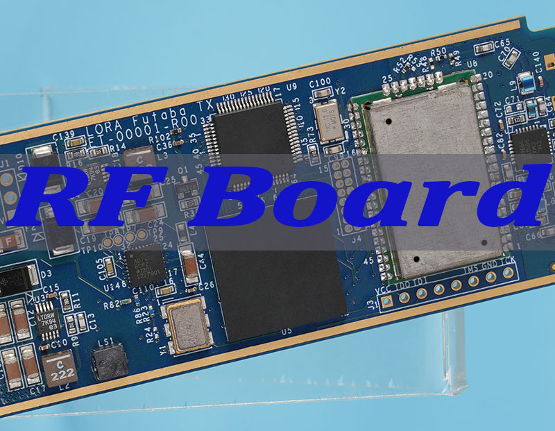
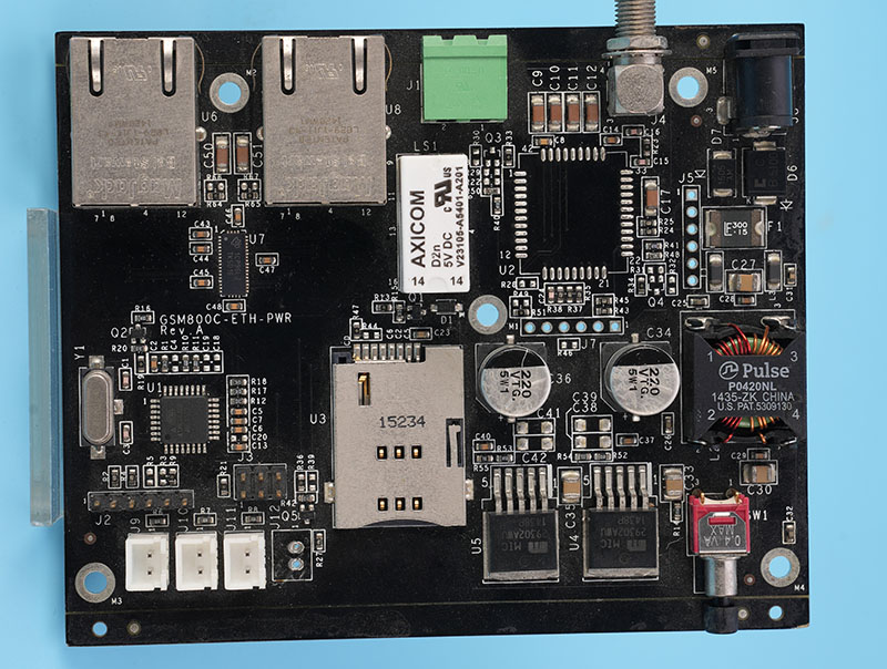
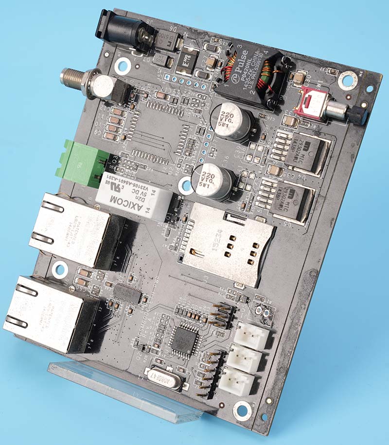
RF circuit board is the backbone of any system transmitting or receiving radio frequency signals, forming the critical physical link between components in wireless communication, radar, and high-speed digital applications. This article delves into the specialized world of RF PCB design, materials, manufacturing, and testing, providing a comprehensive guide for engineers seeking reliable, high-performance custom RF circuit board solutions.
As RF performance requirements tighten, the limitations of conventional PCB manufacturing quickly surface in real hardware.
- Unpredictable Signal Loss & Performance: Variations in dielectric consistency and copper surface quality cause excessive attenuation and reduced system range.
- Impedance Mismatch & Signal Reflection: Minor trace or material Dk deviations lead to reflections that degrade RF efficiency and stability.
- Signal Integrity & Crosstalk at High Frequencies: Poor isolation and stack-up planning introduce EMI and coupling issues in multi-GHz designs.
- Thermal Management & Reliability Issues: Inadequate heat dissipation and CTE mismatch result in delamination and long-term RF failure risks.
- Long Lead Times & Prototype Iterations: Slow RF prototyping cycles delay validation and significantly extend time-to-market.
To move past these limitations, success depends on working with a manufacturer that combines hands-on practical RF printed circuit board design insight with disciplined process control and fast prototyping execution.
- Engineered Laminate Selection: Low-loss materials such as Rogers, Taconic, or Isola maintain stable Dk/Df across frequency and temperature.
- Precision Controlled-Impedance Fabrication: LDI and fine etching accuracy ensure trace geometry consistency, verified through coupon testing within ±5%.
- Simulation-Driven HDI & Shielding: EM simulation guides stack-up, placement, and shielding to isolate critical RF paths effectively.
- Thermally-Optimized Construction: Metal cores, thermal vias, and matched CTE materials improve heat dissipation and structural reliability.
- Dedicated Quick-Turn RF Prototype Lines: Specialized RF assembly and testing lines enable rapid validation and iterative development.
At BEST Technology, we are a specialized RF PCB manufacturer focused on high-frequency and high-reliability applications. Our core strength lies in providing custom RF circuit board solutions with quick prototypes, bridging the gap between complex design and volume production. We combine state-of-the-art process controls with deep material science expertise to ensure your RF circuit design performs as simulated. A warm welcome to contact our engineering team at sales@bestpcbs.com to start your circuit RF project.

What Is an RF Circuit Board?
An RF (Radio Frequency) circuit board is a specialized printed circuit board designed to carry, route, and process signals in the radio frequency spectrum, typically from about 3 MHz up to several tens of GHz. Unlike standard digital boards, its primary function is to preserve the integrity of high-frequency analog signals, minimizing loss, reflection, and interference.
- Core Function: To provide a controlled electromagnetic environment for signals, acting as a guided medium between antennas, amplifiers, filters, and ICs.
- Key Differentiator: Every physical aspect—material, trace geometry, via structure—is optimized for its electrical performance at the target frequency, not just electrical connectivity.
- Common Applications: Cellular base stations, satellite communications, radar systems, GPS modules, RFID readers, and wireless networking equipment (Wi-Fi/5G).
In essence, an RF PCB is a carefully engineered component where the board itself is part of the circuit’s performance equation.

How Does an RF Circuit Board Differ From Standard PCBs?
The transition from a standard PCB to an RF circuit board represents a shift from treating the board as a simple carrier to treating it as a critical circuit element. The differences are foundational.
| Aspect | Standard PCB | RF Circuit Board |
|---|---|---|
| Primary Material | FR-4 (Epoxy glass) | Specialized laminates (Rogers, PTFE, Ceramic-filled) |
| Design Priority | Connectivity, Routing Density | Signal Integrity, Controlled Impedance, Loss Minimization |
| Trace Geometry | Width based on current carry | Width/Spacing precisely calculated for target impedance (e.g., 50Ω) |
| Grounding | Large ground pours, less critical | Continuous ground planes, strategic via fencing, no ground splits |
| Signal Analysis | DC & Digital Timing | Full-wave S-parameters (S11, S21), EM Field Simulation |
In brief, RF PCBs demand a higher level of material science, precision fabrication, and electromagnetic design rigor, where the RF circuit board material and geometry are inseparable from the circuit’s function.
What Are the Common Types of RF Circuit Board Material?
Material selection is the first and most critical decision in RF design, directly determining loss, stability, and cost.
- FR-4 (Standard & High-Frequency Grades): Cost-effective for lower frequencies (< 1-2 GHz). High-frequency FR-4 offers better Dk stability but higher loss than specialized materials.
- PTFE-Based Laminates (e.g., Rogers RO4000® series): The industry standard for high-performance. Low loss, stable Dk over temperature/frequency, excellent for RF and microwave printed circuit board applications up to 77 GHz.
- Hydrocarbon Ceramics (e.g., Rogers RO3000® series): Very low loss, ultra-stable Dk. Ideal for demanding applications like automotive radar and aerospace where performance cannot drift.
- PTFE Composites: Woven glass or ceramic-filled PTFE offering a good balance of electrical performance, mechanical strength, and cost for mid-range applications.
- Polyimide: Used in flexible RF circuits, offering good high-frequency performance alongside flexibility for dynamic or compact designs.
To wrap up, the choice involves balancing Dielectric Constant (Dk), Dissipation Factor (Df), thermal performance, and cost. For a multi-GHz RF printed circuit board, low-loss PTFE or ceramic-based materials are often mandatory.
What Are the Steps for RF Circuit Board Design?
Successful RF circuit board design is a meticulous, iterative process that integrates simulation deeply into the workflow.
- Define Requirements & Select Material: Determine frequency, bandwidth, power, and impedance. Choose substrate based on required Dk, loss, and thermal performance.
- Schematic Capture with RF Models: Use components with accurate S-parameter or nonlinear models. Incorporate distributed elements (microstrip, stripline) from the start.
- Electromagnetic (EM) Simulation & Layout: Simulate critical structures (transitions, filters) before layout. Place components to minimize path lengths. Use EM solver to define stack-up and trace geometry for controlled impedance.
- Layout with Strict DFM/DFR Rules: Implement continuous ground planes, minimize via stubs, use curved bends (not 90°), and add shielding via fences. Adhere to fabricator’s capabilities for tolerances.
- Post-Layout Simulation & Validation: Run a full-board EM simulation to verify S-parameters, identify unwanted coupling, and predict final performance. This step is non-negotiable for a practical RF printed circuit board design approach.
- Generate Fabrication & Assembly Files: Provide detailed impedance control drawings, material callouts, and assembly notes to the manufacturer.
To summarize, RF design is a simulation-validated, specification-driven process where the layout is an integral part of the circuit simulation itself.
Design Challenges and Solutions in RF and Microwave Printed Circuit Board up to Multi-GHz Ranges
As frequencies venture into the multi-GHz microwave spectrum, RF and microwave printed circuit board design confronts quantum-level physical effects.
- Skin Effect & Conductor Loss. Current crowds at the conductor surface, increasing effective resistance.
- Solution: Specify thick surface finishes (e.g., 2-3x skin depth). Use low-roughness copper foil to reduce surface scattering.
- Dielectric & Radiation Loss. Substrate material absorption and energy radiation from discontinuities become significant.
- Solution: Use ultra-low-loss (low Df) laminates. Enclose critical traces in stripline configurations to contain fields.
- Parasitic Effects. Every discontinuity (via, connector) acts as a parasitic inductor/capacitor.
- Solution: Model all transitions in 3D EM simulators. Use back-drilled, blind, or coaxial vias to minimize stubs.
- Manufacturing Tolerances. A 0.1-mil variation in trace width can shift impedance at 40 GHz.
- Solution: Design with tolerances in mind. Partner with manufacturers like best HDI PCB manufacturers for RF and microwave circuit boards who guarantee tight process controls (e.g., ±0.2 mil etch tolerance).
In summary, overcoming multi-GHz challenges requires a synergy of advanced simulation, careful material science, and partnership with a manufacturer capable of extreme precision.
Manufacturing Capabilities Required by Best HDI PCB Manufacturers for RF and Microwave Circuit Boards
The best HDI PCB manufacturers for RF and microwave circuit boards differentiate themselves through a suite of advanced, tightly controlled capabilities essential for high-frequency success.
| Capability | Why It’s Critical for RF |
|---|---|
| Laser Direct Imaging (LDI) | Achieves the fine line/space resolution (< 3/3 mil) needed for precise controlled impedance in HDI designs. |
| Plasma Etch Desmear | Essential for preparing PTFE (Teflon) materials for reliable plating, preventing via failures. |
| Controlled Depth Drilling & Back-Drilling | Removes the unused via stub (the “antenna”) that causes severe resonance and loss at high frequencies. |
| Advanced Surface Finishes | Offers low-loss options like Electroless Nickel Electroless Palladium Immersion Gold (ENEPIG) or high-quality immersion silver. |
| Tight Process Control & Testing | Maintains impedance tolerance within ±5-10% via in-process testing and dedicated RF circuit board test fixtures. |
To sum up, true RF expertise in manufacturing is defined by precision processes tailored for exotic materials and geometries, not just standard PCB fabrication.
Best HDI PCB Manufacturers for RF and Microwave Circuit Boards
Identifying the best manufacturer goes beyond a capabilities list. Key attributes include:
- Material Expertise: Deep partnerships with laminate suppliers (Rogers, Taconic) and in-house material testing.
- Engineering Support: A team that reviews designs for manufacturability and performance, offering practical RF printed circuit board design advice.
- Dedicated Quick-Turn Prototype Service: The ability to produce complex, high-layer count RF prototypes in days, not weeks, is a hallmark of a true development partner.
- Vertical Integration for RF Assembly: In-house RF circuit board assembly with RF-grade soldering, underfill, and conformal coating ensures total quality control.
- Comprehensive Testing: Investment in network analyzers, TDR, and custom test fixtures to validate S-parameters, not just connectivity.
🏆 Industry Leaders
| Company Name | Board Type | Certifications |
|---|---|---|
| TTM Technologies | RF / Microwave / Aerospace HDI | AS9100, ISO 13485, ISO 9001 |
| Unimicron Technology | Consumer HDI / RF Flex-Rigid | ISO 9001, UL, IATF 16949 |
| High Quality PCB Co., Ltd. | Multilayer HDI / RF | AS9100, ISO 14001, UL, RoHS |
| LT Circuit | RF / Microwave / Telecommunications | ISO 9001, UL, TS 16949 |
| BEST Technology | Advanced HDI / RF Prototyping | ISO 9001, AS9100, ISO 13485, TS 16949, UL, RoHS |
To conclude, the best HDI PCB manufacturers for RF and microwave circuit boards act as an extension of your engineering team, providing the technical partnership and agile manufacturing needed to bring a high-frequency design to life.
What Is a Coupon in an RF Circuit Board?
A coupon, or test coupon, is a dedicated section on the production panel containing duplicate traces and structures of the actual RF board. It is sacrificial and used for destructive and non-destructive testing to verify the manufacturing process without damaging the functional boards.
- Impedance Verification: Contains microstrip and stripline traces of the same geometry as the design, measured with a Time Domain Reflectometer (TDR) to confirm impedance meets spec.
- Material & Process Validation: Used to test laminate Dk/Df, plating quality, and etch accuracy, ensuring the entire batch meets the required electrical standards.
In a nutshell, the coupon is the quality assurance certificate for an RF PCB, providing empirical data that the board was built to the exact electrical specifications.
Critical Testing Considerations in RF Circuit Board Assembly for Stable RF Performance
RF circuit board assembly adds another layer of variables that can degrade performance. Testing must go beyond “opens and shorts.”
- Pre-Assembly Inspection: Verify bare board impedance and loss using coupon data. Inspect for surface defects on pads.
- Solder Paste & Reflow Profiling: Use low-residue, no-clean pastes. Precisely control reflow profiles to prevent thermal shock to sensitive RF components and laminates.
- Post-Assembly RF Testing: Perform functional RF testing (e.g., gain, noise figure, output power) using a test fixture that connects to the board’s RF ports. This is the ultimate validation.
- Environmental Stress Screening (ESS): For critical applications, subject assemblies to thermal cycling and vibration to screen for infant mortality and workmanship issues.
- Conformal Coating Validation: If used, ensure the coating material is RF-transparent (low Dk/Df) and uniformly applied to prevent impedance shifts.
In closing, RF assembly testing is performance-centric, focusing on ensuring the assembled module meets its S-parameter and functional specifications in real-world conditions.
How Engineers Identify, Shield, and Optimize RF Paths on RF Printed Circuit Boards in Complex Systems?
In complex systems, managing RF printed circuit boards involves isolating sensitive RF paths from noisy digital domains.
- Identification & Partitioning. Use schematic and layout tools to highlight all RF nets. Physically partition the board into distinct RF, analog, and digital sections.
- Shielding. Implement “canyons” of grounded shielding vias (stitched at < λ/20 spacing) between sections. For critical circuits like an RF receiver circuit board LNA, use soldered metal shielding cans to create a full Faraday cage.
- Optimization.
- Routing: Keep RF traces short, direct, and on the top layer adjacent to a ground plane. Avoid crossing plane splits.
- Grounding: Use a solid, unbroken ground plane under RF sections. Employ multiple vias to connect ground pours and component pads to the plane.
- Filtering: Use feedthrough capacitors and π-filters at the power entry points to each section to prevent noise coupling via supply lines.
In essence, effective management of RF paths relies on strategic physical partitioning, robust shielding via fences or cans, and meticulous attention to grounding and routing to preserve signal purity.
What Makes EBest Circuit (Best Technology) the Optimal RF Printed Circuit Boards Supplier?
EBest Circuit (Best Technology) stands out as a premier RF PCB supplier by combining nearly two decades of specialized manufacturing experience with rigorous, data-driven process capabilities. Our optimal service is built on four key pillars:
1. Deep Technical Expertise and Material Mastery
- Specialized Materials: We are experts in processing high-frequency materials essential for RF performance, including Rogers (e.g., RO4003, RO4350B) and PTFE (Teflon), as documented in our capabilities.
- Proven Process Control: RF boards require complex copper plating and precise fabrication. Our experienced engineers successfully manage these challenges, ensuring reliable plated through-holes and consistent performance. Our certifications (ISO9001, IATF 16949) underscore our commitment to quality.
2. Advanced and Quantifiable Manufacturing Capabilities
Our technical specifications, validated by our equipment, provide tangible evidence of our ability to meet demanding RF designs:
- High-Precision Fabrication: We achieve fine lines/spaces down to 2.5/2.5 mil for inner layers and 3/3 mil for outer layers, crucial for controlled impedance and signal integrity.
- Laser Drilling Technology: We support advanced HDI designs with laser-drilled micro-vias as small as 0.07mm.
- Impedance Control: We guarantee tight impedance tolerances of ±5Ω (for values <50Ω) or ±10% (≥50Ω), ensuring your RF circuits perform as designed.
- Board Size and Thickness: We handle a wide range of requirements, from 3x3mm prototypes to large-format arrays up to 610x610mm, with board thicknesses from 0.15mm to 10mm.
3. Speed and Flexibility from Prototype to Production
- Rapid Prototyping: We understand the iterative nature of RF design. Our expedited services can ship urgent 1-2 layer RF prototypes within 24 hours, allowing for quick testing and validation.
- Seamless Scaling: With a massive monthly production capacity of 28,900 square meters, we ensure a smooth transition from prototype to mass production without compromising quality or lead times, supported by a 97% on-time delivery rate.
4. True Partnership and Comprehensive Turnkey Solutions
- Engineering Support: We go beyond manufacturing by offering engineering and DFM feedback, acting as an extension of your R&D team to de-risk designs.
- Full Turnkey Service: We provide a complete solution, from PCB fabrication and component sourcing to assembly (PCBA) and final box build, simplifying your supply chain.
Overall, EBest Circuit (Best Technology) is the optimal partner because we deliver more than just boards; we deliver certified quality, proven technical capability, and a collaborative partnership focused on accelerating your RF product’s success.

In conclusion, RF circuit board is the foundational platform that determines the ultimate performance and reliability of any wireless or high-speed system. This guide has explored the critical aspects of RF PCBs, from material science and design principles to advanced manufacturing and testing.
Success in this demanding field requires a partner with the right blend of expertise, precision, and speed. BEST Technology is committed to being that partner, providing custom RF circuit board solutions with quick prototypes to accelerate your RF circuits Project. For a consultation or quote, please contact our engineering team at sales@bestpcbs.com.
FAQs
How to Identify an RF Antenna on a Circuit Board?
Look for a unique copper trace, often curved, meandered, or forming a patch, typically located on the board’s edge or in a corner. It is usually connected to an RF transceiver chip via a controlled-impedance trace and is isolated from ground pours in its immediate vicinity.
What Is a Radio RF Pass-Through Circuit Board?
It is a specialized board designed solely to route an RF signal from one connector (e.g., on the chassis wall) to another inside an enclosure with minimal loss and reflection. It acts as a high-performance, shielded feedthrough, often using coaxial-like structures within the board.
What Parts of a Circuit Board Confine RF Transmission Signals?
The primary elements are the ground planes above and below the signal trace (in stripline) or below it (in microstrip), which create a controlled electromagnetic field. Additionally, shielding via fences running alongside the trace form a waveguide-like structure that confines the field and prevents radiation and crosstalk.


