

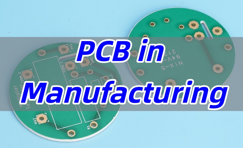
PCB in manufacturing plays a critical role in today’s electronic industry. This blog provides a comprehensive guide to PCB manufacturing, covering materials, technologies, machinery, step-by-step production processes, testing methods, and practical tips for selecting and sourcing reliable PCB manufacturers in China.
Are you facing any of the following challenges when looking for a reliable PCB manufacturer?
- Attractive low quotes, but inconsistent quality leads to rework or scrap.
- Poor communication with suppliers, making design or production issues hard to resolve promptly.
- Insufficient technical support, making complex boards or high-frequency PCBs difficult to produce.
- Lack of transparency in materials, processes, and testing, making it hard to control total cost of ownership (TCO).
- High risk when placing large orders without verifying quality and lead times first.
Here’s how EBest Circuit (Best Technology) addresses these common challenges:
- Transparent and reasonable quotes that cover high-quality materials, complete processes, thorough testing, and reliable service to ensure long-term stability.
- Dedicated project managers provide full-process support and English communication, proactively giving DFM feedback and optimization suggestions.
- Technical expertise and design support for high-frequency, HDI, blind/buried vias, and other complex PCB manufacturing.
- Full transparency in materials, processes, and test reports, allowing customers to control TCO and make informed decisions.
- Support for small-batch sample validation and third-party testing, allowing gradual scale-up to full production with minimal risk.
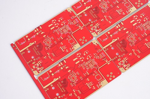
As one of the best PCB manufacturers in China, EBest Circuit (Best Technology) provides full EMS PCB services, including quick prototypes, PCB manufacturing, PCB assembly, and box build service. Our wide product range includes FR4 PCB, flexible circuits, rigid-flex circuits, aluminum PCB LED, and ceramic substrate PCB. We have acquired different experiences in customers’ projects and have provided brilliant PCB and PCBA solutions to our customers in the global market and the Chinese market. If you have any questions or inquiries, please contact us via +86-755-2909-1601 or sales@bestpcbs.com. We will gladly help.
What is PCB in Manufacturing?
Printed Circuit Board, or PCB, is the backbone of modern electronics. When people ask what PCB stands for, the answer is straightforward—Printed Circuit Board. But in manufacturing, it means much more than just a name. It is the essential platform that connects and supports components in nearly every electronic product we use today. Without PCBs, manufacturing electronics would still rely on bulky wiring and manual assembly, which is slow, costly, and unreliable.
Understanding PCBs in Simple Terms
In the simplest sense, a PCB is a thin board made from insulating materials, usually fiberglass or ceramic, with copper layers that form conductive pathways. These copper tracks replace the need for traditional wiring. Components like resistors, capacitors, and chips are mounted directly on the board, and the copper routes connect them into a functioning system.
This simplicity is the reason why PCBs became so popular. They make electronic designs smaller, lighter, and more efficient. That is why you can hold a smartphone in one hand instead of carrying a box full of circuits and wires.
The Key Types of PCBs in Manufacturing
In manufacturing, PCBs are not one-size-fits-all. They come in different structures to serve different needs. Generally, there are three primary types:
- Single-sided PCBs – They have copper traces on one side only. Simple and cost-effective, used in calculators, LED lights, and low-complexity devices.
- Double-sided PCBs – Copper patterns exist on both sides, connected by vias. They support more components in a compact size, common in control systems and consumer electronics.
- Multilayer PCBs – These are stacks of multiple copper and insulating layers, laminated together. They handle complex, high-speed, and high-density designs used in servers, medical devices, and aerospace systems.
This variety shows how PCBs can adapt to both simple gadgets and cutting-edge equipment.
Why PCBs Became the Standard in Manufacturing
The widespread adoption of PCBs in manufacturing was not accidental. There are at least four strong reasons:
- Miniaturization: They reduced the size of electronic products dramatically.
- Reliability: Consistent copper pathways mean fewer connection failures compared to hand-soldered wiring.
- Mass Production: PCBs can be produced in bulk with high accuracy, lowering costs.
- Design Flexibility: Engineers can create intricate circuits that would be impossible with loose wires.
These advantages explain why PCBs moved from laboratories into mass production and became a universal standard.
Everyday Products That Contain PCBs
It’s hard to name a modern product without a PCB inside. Consumer electronics such as smartphones, laptops, and TVs all rely on them. Cars use them for engine control, safety systems, and infotainment units. Medical equipment, from diagnostic tools to life-support systems, depends on PCB reliability. Even household appliances like washing machines and microwaves contain small but critical boards.
This universal presence highlights the importance of PCBs in manufacturing—no matter if the device is simple or complex, a PCB is likely powering it.
Why PCBs Matter in Manufacturing
To sum up, PCB in manufacturing is not just a circuit board; it is the foundation of modern electronic innovation. From single-sided boards in basic products to multilayer structures in advanced systems, PCBs make production practical, scalable, and reliable. They replaced traditional wiring with something faster, more compact, and easier to reproduce. Their popularity lies in simplicity, flexibility, and the ability to serve almost every industry.
Electronics without PCBs would still be large, fragile, and inconsistent. With them, manufacturers create everything from affordable gadgets to mission-critical aerospace systems. This is why PCBs are the true silent force behind our connected world.
What are the Technologies Used in PCB Manufacturing?
Modern PCB fabrication has advanced far beyond simple copper patterning. Today, manufacturers leverage a suite of cutting-edge technologies to meet the demands of high-density, high-speed, and high-reliability electronic systems.
1. Photolithography and Laser Direct Imaging (LDI)
Photolithography remains a cornerstone in PCB production. It transfers circuit patterns from CAD files to copper-clad laminates using UV light and photoresist. To achieve finer lines and spaces for high-density interconnect (HDI) boards, laser direct imaging (LDI) is increasingly employed. LDI provides superior precision, reduces alignment errors, and shortens production cycles, particularly for line widths below 50 μm, which is critical for HDI/BUM and chip-scale packaging PCBs.
2. Microvia and Laser Drilling Technologies
The trend toward smaller vias is driven by the integration density of modern ICs. Mechanical drilling has limits, typically above 100 μm. For microvias and blind/embedded vias, CO₂ and UV laser drilling are widely used. UV lasers can create vias smaller than 50 μm with minimal thermal damage, while CO₂ lasers are effective for slightly larger microvias and high-throughput production. Hybrid laser systems combine the advantages of both to improve efficiency and accuracy.
3. High-Density Multilayer Lamination
As IC complexity grows, PCBs have evolved from simple single-layer boards to multilayer HDI structures. Modern lamination integrates multiple copper-clad laminates, often using sequential lamination for buried and blind vias. Layer-to-layer registration precision has become crucial, with tolerances controlled to a few microns to ensure signal integrity and reliable interconnects. Advanced dielectric materials with low coefficient of thermal expansion (CTE) and tailored Tg values help maintain layer alignment under thermal stress.
4. Fine Line and Conductor Technology
Conductor miniaturization is essential for high-speed and high-frequency designs. Line widths have evolved from 100 μm to as narrow as 8–10 μm. Achieving such precision requires ultra-thin copper foils, improved etching techniques, and strict surface treatments. Uniform copper distribution, high-resolution photoresists, and vacuum or rapid etching systems ensure line width tolerance and prevent defects such as over-etching or rough edges, which can cause signal degradation.
5. Surface Finish and Pad Coating Technologies
Surface finishing technologies ensure solderability and long-term reliability of PCBs. Traditional HASL (Hot Air Solder Leveling) has given way to more precise techniques like OSP (Organic Solderability Preservatives), chemical Ni/Au, and Pd/Au coatings. These coatings protect copper pads from oxidation, provide flat surfaces for fine-pitch SMT assembly, and enable high-temperature soldering required for lead-free processes. Pd and Au layers also support wire bonding and fine-pitch connections.
6. Advanced CCL Materials
Copper-clad laminate (CCL) materials have evolved to support HDI and high-performance applications. High Tg, low CTE, and uniform dielectric layers help manage thermal expansion and prevent CAF (Conductive Anodic Filament) formation. Special CCLs, including flat E-glass fabrics and metal-core laminates, improve laser drilling performance, reduce surface roughness, and support high-density fine-line PCB fabrication. Low and high dielectric constants are tailored for RF/microwave applications and embedded passive components.
7. Automation and Robotics in PCB Manufacturing
Automation plays a critical role in modern PCB production. Automated assembly lines, robotic drilling, and pick-and-place machines ensure consistent quality and reduce human error. High-density SMT assembly, precise component placement, and in-line inspection systems allow manufacturers to handle complex boards efficiently while meeting tight tolerances for HDI and multilayer PCBs.
8. Trends Driving PCB Technology
PCB technology development is closely tied to IC integration and system miniaturization. Microvia adoption, ultrafine lines, multilayer HDI structures, and embedded components address high-density requirements. Materials science advances, including high Tg, low CTE laminates, and improved surface finishes, support higher frequency, higher power, and higher reliability applications. Laser-based processes and LDI enable precise manufacturing for emerging electronics in telecommunications, aerospace, automotive, and medical devices.
What are the PCB Manufacturing Machines?
Modern PCB factories are equipped with a comprehensive set of machines, covering every stage from raw material processing to final inspection. Each machine plays a crucial role in ensuring precision, efficiency, and product reliability.
1. CNC Drilling Machines
Used to drill through-holes and vias on PCBs. CNC drilling machines provide precise control over hole size and placement, ensuring reliable interconnections for multilayer boards. Modern high-precision CNC machines can handle microvias with diameters smaller than 100 μm.
2. Laser Drilling Machines
Used for microvias and high-density boards. UV lasers can create vias smaller than 50 μm with minimal thermal damage, making them ideal for HDI and chip-scale package PCBs. CO₂ lasers are effective for slightly larger microvias and high-throughput production.
3. Imaging / LDI Machines
Include traditional photolithography and Laser Direct Imaging (LDI) systems that transfer circuit patterns to copper-clad laminates. LDI offers higher precision and is particularly suited for ultrafine lines and high-density interconnect boards.
4. Etching Machines
Remove excess copper to reveal the circuit pattern. Modern etching machines use chemical or vacuum etching to maintain line width tolerance, prevent over-etching, and ensure smooth edges, which is critical for high-speed signal integrity.
5. Solder Paste Printers
Accurately apply solder paste to PCB pads for SMT assembly. High-precision printers can handle ultra-fine pitch components, as small as 0.3 mm.
6. Dispensing Machines
Apply localized coatings such as protective varnish, conductive adhesives, or thermal interface materials (TIM) to specific PCB areas to enhance reliability.
7. Pick-and-Place Machines
Rapidly and precisely place SMD components on the PCB, forming the core of modern SMT production lines.
8. Reflow Ovens
Used to solder SMD components by melting solder paste uniformly and cooling it properly, ensuring strong and reliable joints.
9. Wave Soldering Machines
Mainly used for through-hole components, especially in mixed-technology boards that combine SMT and PTH components.
10. Automated Optical Inspection (AOI) Machines
Detect defects such as opens, shorts, misaligned components, or solder issues to improve yield and product quality.
11. Solder Paste Inspection (SPI) Machines
Check solder paste printing quality, including volume, position, and shape, to prevent placement defects in later assembly steps.
12. Flying Probe Testers
Used for small-volume or prototype PCBs to verify electrical connectivity and detect shorts without requiring a custom test fixture.
13. In-Circuit Test (ICT) Machines
Test electrical performance in mass production, verifying component placement, solder quality, and circuit integrity.
14. Surface Finish Equipment
Includes chemical Ni/Au plating, OSP, chemical Sn/Pb, and other finishes to protect pads from oxidation and ensure long-term reliability.
15. Solder Mask Printers
Apply protective coatings on PCB surfaces, preventing shorts and oxidation while leaving precise pads exposed for SMT assembly.
16. Cleaning Machines
Remove flux residues, chemical contaminants, or dust to ensure clean PCB surfaces and enhance product reliability.
17. X-ray / Advanced Optical Inspection (AXI) Machines
AXI complements AOI by inspecting hidden joints, such as BGA or embedded components, to ensure internal soldering quality.
18. Routing, V-Cut, and Laser Cutting Machines
Separate panels into individual boards, providing smooth edges and burr-free cuts.
19. Automated Storage and Handling Systems
Connect production stages, enabling automated PCB transport, stacking, and sorting, improving overall factory efficiency.
What is the Difference Between FR-4, High-Tg, and High-Frequency PCB Materials?
At EBest Circuit (Best Technology), we often get asked: “Which PCB material should I choose?” To answer this, we like to start with a simple analogy that makes the differences crystal clear.
Think of PCB materials as vehicles on a road:
- FR-4 is like a family sedan. Reliable, affordable, and perfectly adequate for most everyday needs. It’s our default recommendation unless your design has special demands.
- High-Tg FR-4 is like a high-performance SUV or off-road vehicle. Tougher, more heat-resistant, and designed to handle extreme environments. Ideal when your PCB faces high temperatures or long-term heavy loads, such as in automotive engine compartments or high-power power supplies.
- High-frequency materials are like a race car or optical fiber. Optimized for speed and precision, minimizing signal loss. They are essential for RF, microwave, or high-speed digital circuits where signal integrity cannot be compromised.
Material Comparison Table
To help you decide, here’s a direct comparison of the key parameters:
| Key Parameters | Standard FR-4 | High-Tg FR-4 | High-Frequency Materials |
|---|---|---|---|
| Glass Transition Temperature (Tg) | ~130–140°C | >170°C | Varies, generally high |
| Dielectric Constant (Dk) | ~4.5 | ~4.5 | 2.5–3.5 (lower and more stable) |
| Loss Tangent (Df) | ~0.02 | ~0.02 | <0.004 (much lower) |
| Material Cost | Low | Medium | High |
How to Choose the Right Material?
At EBest Circuit (Best Technology), we advise our customers based on the specific environment, electrical requirements, and cost constraints.
1. When FR-4 is sufficient:
- Product examples: Household electronics, toys, phone chargers, internal test boards.
- Reasoning: Operating temperature is below 100°C, signal frequency is low (<1GHz), and cost is the main consideration.
2. When you must upgrade to High-Tg FR-4:
- Product examples: Automotive engine control units, high-power LED lighting, high-density servers.
- Reasoning: Lead-free soldering requires higher reflow temperatures. Devices may operate in high-temperature environments. Long-term reliability is critical.
3. When high-frequency materials are non-negotiable:
- Product examples: 5G base station antennas, microwave and millimeter-wave devices, satellite receivers, high-speed server motherboards.
- Reasoning: Extremely high operating frequencies demand excellent signal integrity and low loss. If your design reaches GHz frequencies, this is a must, not an option.
Practical Tips & Cost Considerations
- Avoid over-design: Using high-frequency laminates for low-speed circuits dramatically increases cost without benefit.
- Mind overall manufacturing cost: High-Tg or high-frequency materials are more expensive, and processing can be more challenging, which may increase total PCB cost.
- Consult early with your manufacturer: Sharing your Gerber files and application requirements early helps EBest Circuit (Best Technology) suggest the most appropriate material, balancing performance and budget.
In a nutshell, choosing the right PCB material is like picking the right vehicle for a journey. FR-4 for everyday tasks, High-Tg FR-4 for extreme conditions, and High-Frequency materials for ultra-speed applications. At EBest Circuit (Best Technology), we act as your trusted advisor, guiding you through material selection to optimize performance, cost, and reliability.
How is a PCB Manufactured Step by Step?
At EBest Circuit (Best Technology), PCB manufacturing follows a rigorously controlled process to ensure every board meets design specifications and quality standards. Here is the step-by-step workflow for a typical four-layer PCB:
1. Material Preparation (Cutting the Base Material)
We start by cutting copper-clad laminates to precise dimensions. Proper preparation ensures uniform thickness and reduces material waste during the process.
2. Inner Layer Imaging (Exposure → Development → Etching)
The inner copper layers are patterned using photolithography. Engineers apply photoresist, expose the design using UV light, develop the pattern, and etch away excess copper to reveal the inner circuitry.
3. Inner Layer Inspection (AOI)
Automated Optical Inspection (AOI) is performed to detect defects such as shorts, opens, or pattern misalignment. This early check prevents costly errors in subsequent steps.
4. Lamination
Multiple layers are stacked and pressed together under heat and high pressure. For four-layer boards, precise layer alignment is critical to maintain electrical performance and signal integrity.
5. Drilling
Holes for vias and component leads are drilled with CNC machines. At EBest Circuit (Best Technology), we use high-precision drilling to achieve exact diameter tolerances and positioning.
6. Copper Plating and Electrical Testing of the Board (Through-Hole Metallization + Panel Electric Test)
Drilled holes are plated with copper to electrically connect layers. After plating, a board-level electrical test is performed to verify continuity and detect potential short circuits.
7. Outer Layer Imaging (Exposure → Development → Etching)
Outer copper layers are patterned using photolithography, following the same exposure, development, and etching steps as the inner layers. This step defines the complete circuit layout.
8. Outer Layer Inspection (AOI)
Another round of AOI ensures the outer layer traces are free from defects, maintaining high yield rates and reliability.
9. Solder Mask Application (Exposure → Development)
A protective solder mask is applied to prevent accidental short circuits and oxidation of the copper traces. Precise mask registration is critical for fine-pitch components.
10. Silkscreen (Legend/Character Printing)
Component markings, logos, and identification codes are printed on the board. This step facilitates assembly and future maintenance.
11. Pre-Baking (Drying/Board Baking)
Boards undergo controlled baking to remove moisture and stabilize the material before surface finishing.
12. Surface Finishing
Pads and exposed copper areas are treated with surface finishes such as HASL, ENIG, or OSP to improve solderability and protect against oxidation.
13. Board Profiling and Cutting (V-Scoring/Route Cutting)
The panel is cut or scored into individual boards with precise dimensions, ensuring clean edges and proper fit in assemblies.
14. Electrical Testing (E-Test/Flying Probe)
Each finished board undergoes a final electrical test to verify connectivity and functionality.
15. Final Quality Control (FQC)
Boards are visually inspected and subjected to final checks to ensure they meet all design and quality requirements.
16. Packaging and Storage
Completed PCBs are carefully packaged to prevent damage during transportation and stored in controlled conditions until shipment.
This workflow highlights EBest Circuit (Best Technology)’s meticulous approach to PCB manufacturing, combining advanced equipment, stringent quality control, and experienced engineering to ensure every board performs reliably in its intended application.
How to Test PCB in Manufacturing Process?
Testing is a critical step in PCB manufacturing to ensure each board’s electrical performance, physical reliability, and long-term stability. PCB testing is a multi-dimensional, staged quality assurance system, covering everything from bare boards to fully assembled products. The core process and key testing methods are summarized below.
1. Overview of the Testing Process: Four Key Stages
The PCB testing process follows a complete closed-loop workflow, allowing issues to be detected and addressed promptly:
- Preparation Stage
- Equipment and Program Setup: Determine the testing strategy based on PCB design requirements (layer count, trace density, functionality). Prepare the necessary testing equipment (e.g., AOI, flying probe testers, functional testers) and fixtures. Develop detailed test programs with parameters and acceptance criteria.
- PCB Pre-Inspection: Conduct a visual check to ensure no mechanical damage, shorts, opens, or component misplacement/missing. For reliability tests, boards may be pre-baked to remove moisture and prevent delamination during testing.
- Testing Execution Stage
This stage is the core of quality control and includes multiple types of tests:- Bare Board Testing: Performed before component assembly, using flying probe or bed-of-nails testers to ensure 100% electrical connectivity with no opens or shorts.
- Assembled Board Testing:
- Visual Inspection (AOI): Check solder joint quality, component placement, and polarity.
- Electrical Performance Tests: Measure insulation resistance, dielectric strength, and continuity.
- Functional Testing (FCT): Simulate real operating conditions to verify full-board functionality for complex boards.
- Reliability Testing: Critical for long-term quality assurance, usually conducted on samples according to standards (IPC). Tests simulate extreme environmental conditions to assess durability and lifespan.
- Analysis and Handling Stage
- Result Analysis: Review test data to identify defect types and severity, including whether issues are due to materials, processes, or design.
- Defect Handling: Mark, isolate, and address non-conforming boards through solder rework, component replacement, or trace adjustment. Feedback is provided to production for process improvement.
- Wrap-up and Improvement Stage
- Data Archiving: Organize and store all test data, programs, and reports to maintain traceable quality records.
- Equipment Maintenance: Clean and calibrate testing equipment to ensure ongoing accuracy.
- Continuous Improvement: Review lessons learned to optimize PCB manufacturing and testing processes, enhancing overall quality.
2. Key Reliability Tests (Manufacturing “Stress Tests”)
These tests evaluate whether PCBs can withstand environmental, thermal, and operational stresses.
- Solderability Test (J-STD-003)
- Purpose: Verify that PCB pads and via surfaces (e.g., ENIG, HASL) form reliable solder joints.
- Method: Immerse the sample in molten solder at 235℃ for 3 seconds.
- Standard: ≥95% pad wetting; plated through-holes must be fully filled with solder.
- Thermal Stress Test (IPC-TM-650 2.6.8)
- Purpose: Simulate high-temperature soldering to evaluate copper-to-substrate adhesion and delamination resistance.
- Method: Immerse the sample in 288℃ molten solder for 10 seconds.
- Standard: No delamination, bubbling, or whitening on the surface.
- Ionic Contamination Test (IPC-TM-650 2.3.25)
- Purpose: Measure residual ionic contamination (flux residues, salts) that could cause leakage or corrosion.
- Method: Extract ions using 75% isopropyl alcohol and measure solution conductivity.
- Standard: ≤6.45 μg NaCl/cm².
- Dielectric Withstanding Voltage Test (IPC-TM-650 2.5.7)
- Purpose: Verify insulation between conductors (traces, layers) under high voltage.
- Method: Apply 500VDC between conductors for 30 seconds.
- Standard: No arcing, breakdown, or flashover.
- Peel Strength Test (IPC-TM-650 2.4.8)
- Purpose: Quantify copper-to-substrate bonding strength.
- Method: Use a peel tester to remove a copper strip vertically.
- Standard: ≥1.1 N/mm to ensure copper adhesion.
- Material Property Tests
- Tg (Glass Transition Temperature): Measured with DSC to determine substrate thermal stability. High Tg supports high-temperature processes such as lead-free soldering.
- CTE (Coefficient of Thermal Expansion): Measured with TMA to evaluate dimensional changes under heat; excessive Z-axis CTE can cause via cracking.
- Time-to-Delamination Test: Heat samples to 260℃ and maintain temperature, recording time to delamination; longer times indicate superior thermal reliability.
To conclude, PCB testing in manufacturing is more than a simple pass/fail check; it is a comprehensive quality management system:
- 100% inspection (electrical tests, AOI) eliminates defective boards from every batch.
- Sampled reliability tests monitor process stability and material quality, evaluating long-term lifespan and reliability while preventing batch-level defects.
By combining structured testing workflows with standardized reliability verification, manufacturers like EBest Circuit (Best Technology) ensure not only that boards function correctly at shipment but also maintain stable performance throughout their lifecycle, building customer trust and brand reputation.
How to Select the Suitable PCB Manufacturing in China?
When sourcing PCB manufacturers in China, clients often worry about three things: stable quality, smooth communication, and hidden issues that could increase costs.
1. Total Cost (TCO)
- Core idea: Extremely low quotes often mean compromises in materials, processes, or testing. Potential risks include:
- Low-grade materials affecting reliability
- Reduced testing allowing defective boards to pass
- Insufficient after-sales support, leaving you to handle issues
- Practical advice: Evaluate quotes alongside process and testing scope, and choose a price that ensures necessary quality safeguards.
2. Certifications and Track Record
- Core idea: Claims like “high quality” or “advanced equipment” mean little—verifiable evidence is key.
- Practical advice:
- Check international certifications: ISO 9001, IATF 16949 (automotive), ISO 13485 (medical), UL
- Review past successful projects, especially for boards similar to your products
- Request transparent test reports: electrical tests, impedance logs, AOI inspection records
3. Communication
- Core idea: Poor communication is a major cause of failure in overseas projects.
- Practical advice:
- Confirm the supplier provides a dedicated project manager or a single point of contact
- Evaluate DFM feedback capability to identify design issues early
- Check frequency and transparency of progress updates to ensure production is under control
4. Technical Expertise & Process Capability
- Core idea: A technically strong supplier can help optimize designs and improve yield.
- Practical advice:
- Verify if the supplier provides materials recommendations and solutions for complex process issues
- Ensure your engineering team can communicate directly with their engineers
- Confirm support for advanced boards such as high-frequency, HDI, and blind/buried via designs
5. Verification Strategy
- Core idea: Avoid placing a large order upfront; validate quality and service first.
- Practical advice:
- Start with a small sample order to evaluate quality, communication, and lead time
- Consider third-party testing: cross-section analysis, thermal stress tests, etc.
- Scale production gradually after sample validation
In summary, don’t just focus on price; also consider quality assurance, transparent communication, technical support, and a controlled validation path. Following these principles helps you avoid common pitfalls in overseas procurement and ensures smooth project delivery.
Where to Get PCB Manufacturing in China?
China has become the global hub for PCB production, but not all suppliers can meet strict quality, reliability, and communication requirements. Selecting the right partner is crucial to avoid hidden costs, project delays, and poor-quality boards. Here’s how EBest Circuit (Best Technology) helps customers navigate these challenges.
Transparent Value and Reliable Quality: We understand that cost is important, but we focus on true value. Our quotes are transparent and reasonable, covering high-quality materials, complete manufacturing processes, thorough testing, and reliable service. By choosing us, customers secure long-term reliability and stability, avoiding hidden costs caused by ultra-low-price suppliers.
Verified Certifications and Evidence: We hold ISO 9001, IATF 16949 (automotive), ISO 13485 (medical), and UL safety certifications. Every PCB batch comes with electrical test reports, impedance logs, and AOI inspection records. Customers can directly verify our certifications, test reports, and successful project examples, ensuring that each board meets high-quality standards.
Clear and Responsive Communication: We assign each customer a dedicated, English-fluent project manager who handles the full process—from quotation and engineering confirmation to production follow-up. We provide proactive DFM feedback, highlight potential design issues, offer optimization suggestions, and regularly update production progress, ensuring customers stay informed and in control.
Technical Expertise and Design Support: We act as a technical partner. Our engineering team provides materials selection advice and process solutions for high-frequency, HDI, blind/buried via, and copper thickness challenges. Customers can communicate directly with our engineers to ensure designs are accurately implemented and yields are optimized.
Low-Risk Validation Strategy: We support small batch sample orders and allow third-party reliability verification. Once the samples pass, we help scale production gradually from trial to full-volume runs. This approach lets customers verify our quality, speed, and communication with minimal risk. We earn trust through facts and performance, not empty promises.
To sum up, EBest Circuit (Best Technology) combines transparent pricing, verified quality, clear communication, technical expertise, and low-risk validation strategies to ensure reliable, long-term partnerships. Choosing us helps customers achieve smooth project delivery, reduced risk, and consistent board performance.
Cases of PCB in Manufacturing in EBest Circuit (Best Technology)
In this case, our precision PCB products were successfully deployed in the innovative product line of a leading communication equipment manufacturer, serving as the critical foundation for their cutting-edge indoor and outdoor high-speed wireless connectivity solutions.
Powering Cutting-Edge Technology:
- Indoor Li-Fi Solution: Our PCB was utilized as the mainboard in the client’s high-speed Li-Fi access points and USB dongles. This application demanded a board capable of stably supporting high-speed bidirectional data transmission up to 1 Gbps and managing complex signals for multi-user access and seamless handover. Our superior PCB design ensured excellent signal integrity, delivering the low-latency, high-throughput performance required for reliability.
- Outdoor Wireless Backhaul System: Within the client’s “High-Speed Backhaul Solution,” our high-frequency PCBs were integrated into the outdoor units. This scenario presented extremely rigorous requirements for stability, interference resistance, and ability to withstand environmental factors, necessitating a PCB that could guarantee consistent 1 Gbps throughput and ultra-low latency of 1-2 ms over long-distance transmissions. Our mature manufacturing processes ensure long-term, stable operation in diverse outdoor conditions.
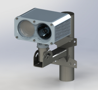
This case demonstrates that our PCBs fully meet the demanding requirements of next-generation communication equipment for high speed, exceptional stability, high-density integration, and complex signal processing. Whether for indoor Li-Fi devices or backhaul systems built for harsh outdoor environments, our products serve as the reliable, “invisible backbone” of our client’s solutions.
In closing, PCB in manufacturing is more than just circuit boards; it is the backbone of electronics. With evolving technologies, advanced machines, and carefully chosen materials, PCBs keep products reliable and scalable. Testing methods prevent failures before they reach users. Pls send us an email at sales@bestpcbs.com if you are looking for the best PCB manufacturer in China. It is our pleasure to give our full engagement to your projects.
FAQs
Q1: What is routing in PCB manufacturing?
A: Routing in PCB has two contexts:
- Design stage routing: This refers to drawing the electrical connections on the PCB, determining how components are electrically linked. It is a critical step that affects PCB performance, including stability, signal quality, and interference resistance.
- Manufacturing stage routing: This is the process of cutting the PCB outline from a larger production panel, creating the final board shape using CNC machines.
In daily communication, when discussing PCB design and functionality, routing usually refers to the “trace routing” on the board.
Q2: What is a BOM in PCB manufacturing and design?
A: A BOM (Bill of Materials) is a detailed list of all components, materials, and specifications required to assemble a PCB, ensuring accurate sourcing and production.
Q3: What is counterbore in PCB manufacturing?
A: Counterbore is a mechanical feature in PCB manufacturing that enlarges the top portion of a drilled hole, allowing components, screws, or nuts to sit flush with the PCB surface, ensuring mechanical stability and assembly flatness.
Application scenarios:
- When a design includes a counterbore, PCB manufacturers typically perform two drilling steps:
- Drill the through-hole using a standard drill bit.
- Use a larger flat-bottom drill or end mill to create a cylindrical recess at the top of the hole.
- Counterbores ensure screws or nuts are flush with the board, improving stability and reliability of the assembled device.
Key differences from countersink holes:
- Purpose: Counterbore allows screws or nuts to sit flush; countersink allows conical screw heads to be level with the board.
- Shape: Counterbore is cylindrical; countersink is conical.
- Screw type: Counterbore suits pan-head screws or nuts; countersink suits flat-head screws.
Q4: What is a via in PCB manufacturing?
A: A via is a plated hole that electrically connects copper layers in a multilayer PCB, enabling signals or power to pass between different layers.
Q5: What is chemical etching in PCB manufacturing?
A: Chemical etching is the process of using acid or alkaline solutions to remove unwanted copper from a PCB, leaving only the desired circuit pattern.
Q6: What is edge plating in PCB manufacturing?
A: Edge plating involves coating the side edges of a PCB with copper, improving conductivity, grounding, and mechanical strength, often used in high-frequency or connector boards.