Why do HDI & high TG PCB solutions matter so much for high-reliability electronics? Because failures rarely come from a single “big” mistake. They often start from small issues: marginal solder joints, microcracks around vias, drift in impedance, or repeated thermal shock.
An HDI PCB helps by shortening trace length, controlling impedance, and reducing stubs. A high Tg PCB helps by raising the glass transition temperature, so the board structure stays stable under higher reflow and operating temperatures.
When you integrate both, you gain:
- Better control of high-speed signals in dense layouts
- Stronger resistance to repeated lead-free reflow cycles
- Improved reliability in wide temperature ranges
- Smaller, lighter boards that still carry complex circuits
For sectors like automotive ADAS, 5G equipment, and industry automation, this combination is often no longer “nice to have”. It becomes a base requirement.
What Are HDI & High Tg PCB Solutions?
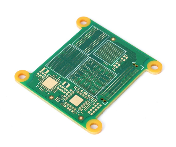
HDI & High Tg PCB solutions refer to PCB designs that use high-density interconnection structures together with high-temperature glass transition materials. Rather than treating HDI PCB and high Tg PCB as separate topics, this concept views them as a design “toolbox” that works as a system.
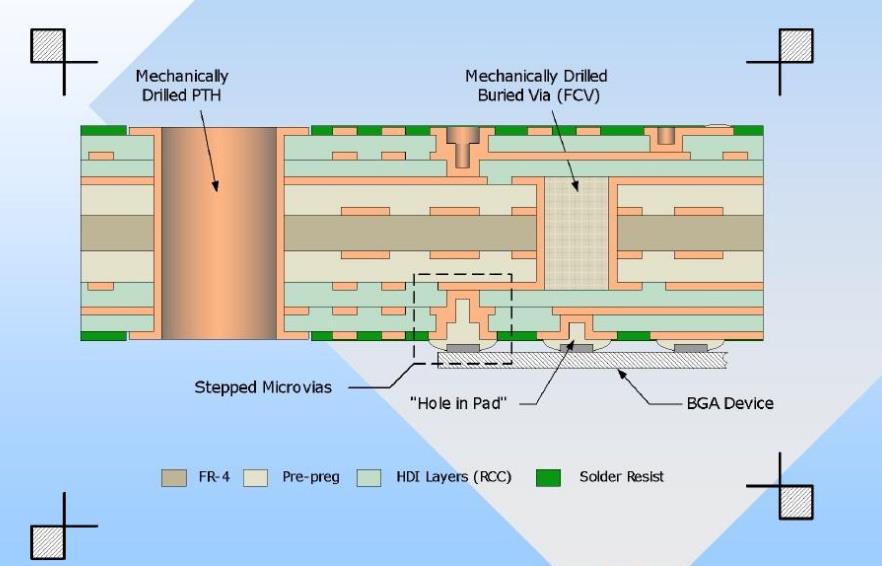
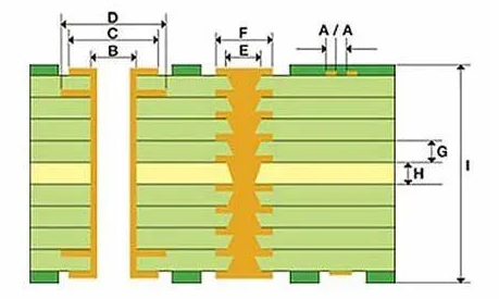
A typical HDI & high Tg PCB stack-up may include:
- High Tg FR4 or hybrid material core
- One or more HDI buildup layers with microvias
- Fine lines and spaces for dense routing
- Controlled impedance structures for high-speed signals
- Multiple lamination cycles using high Tg prepregs
These solutions focus on two goals at the same time: interconnection density and temperature endurance. The design approach covers layout rules, via strategy, material selection, and process limits from the start, not as late-stage fixes.

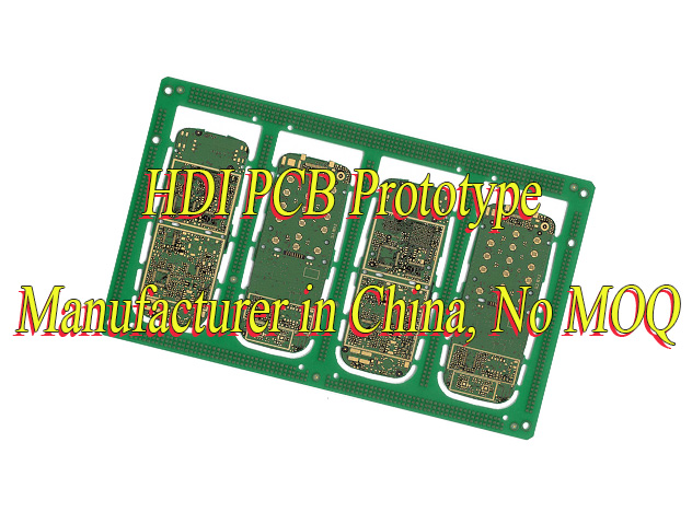
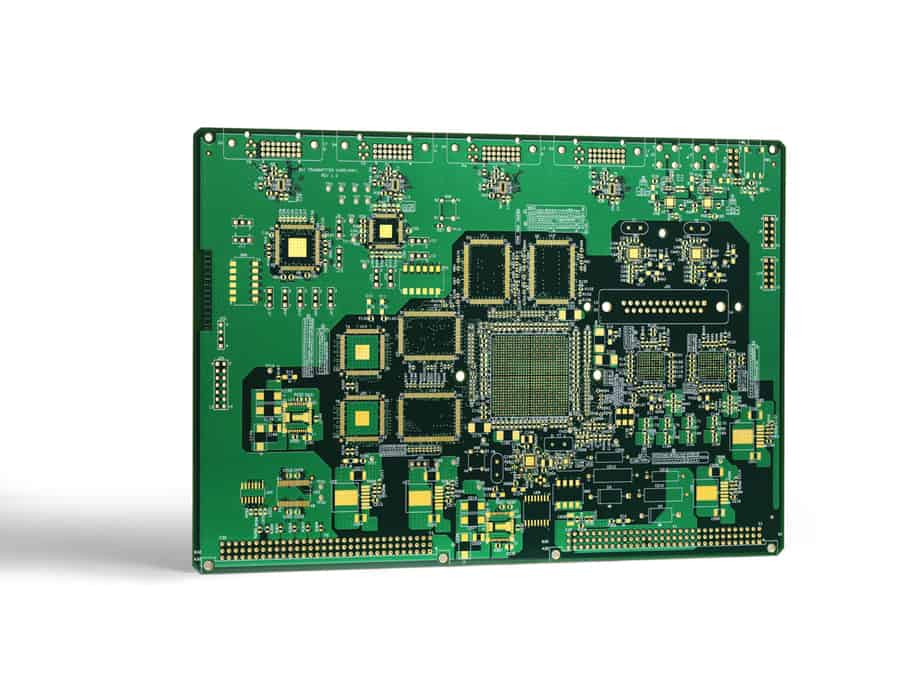
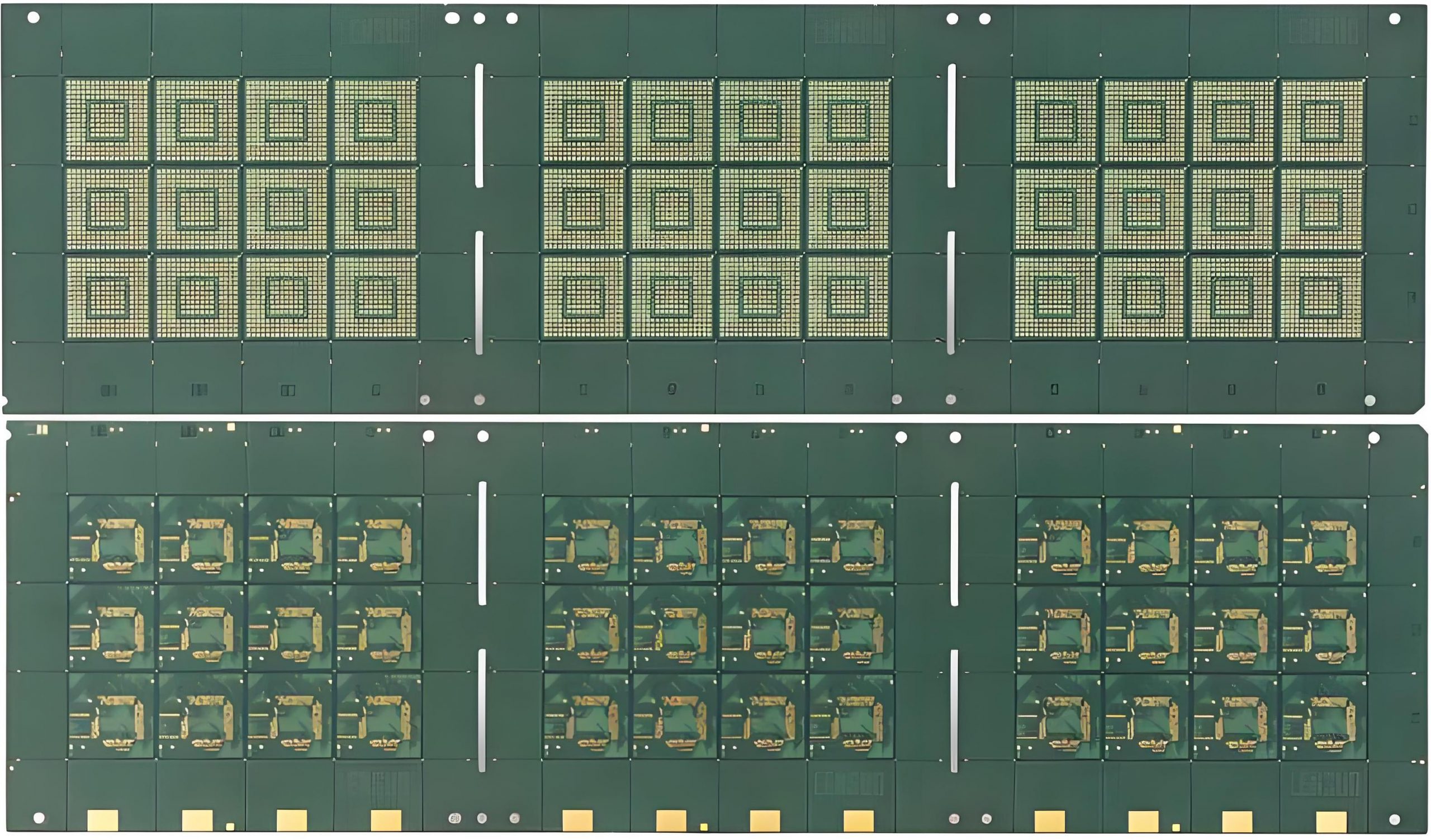
What Is an HDI PCB and Why Is It Used in Modern Electronics?
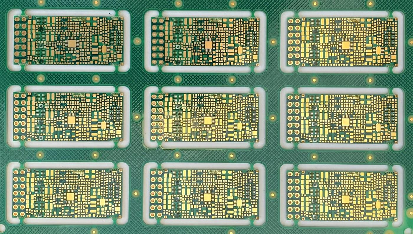
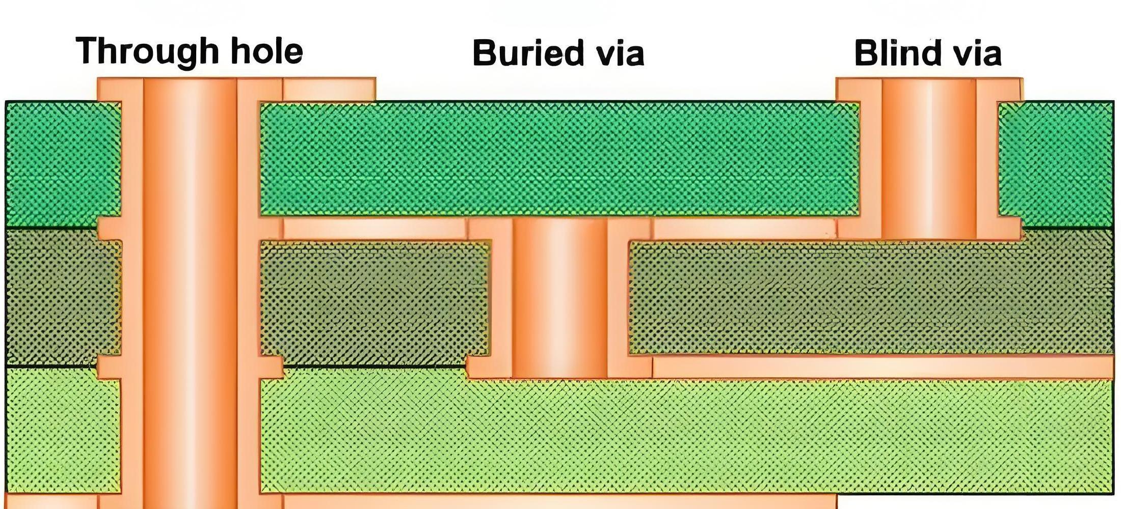
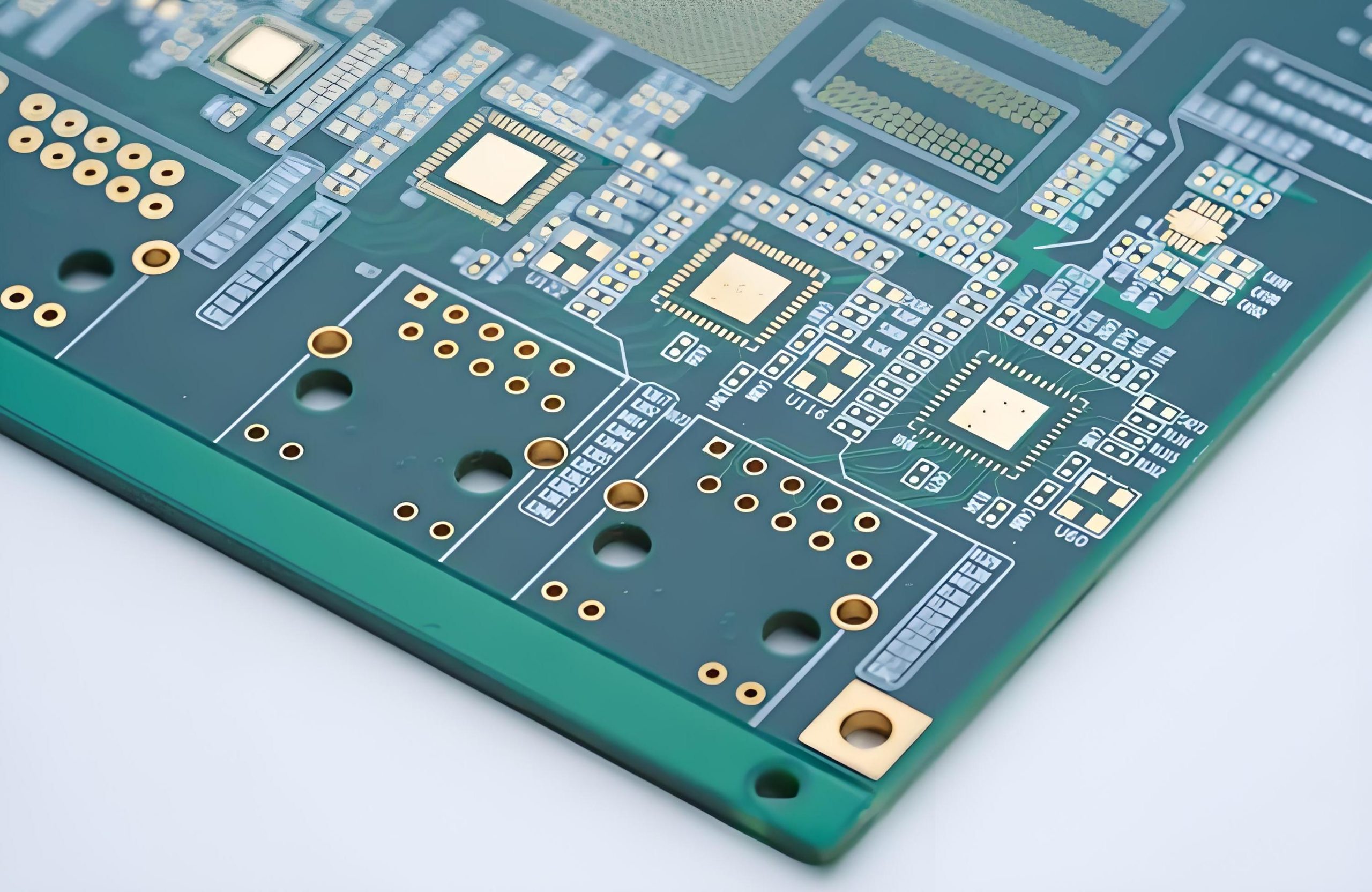
An hdi pcb (High-Density Interconnect PCB) uses finer features and advanced via structures to pack more circuitry into a smaller area. You will often see:
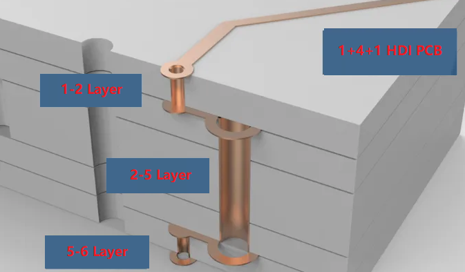
- Microvias (laser-drilled) between layers
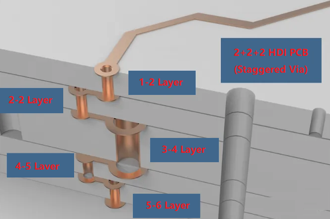
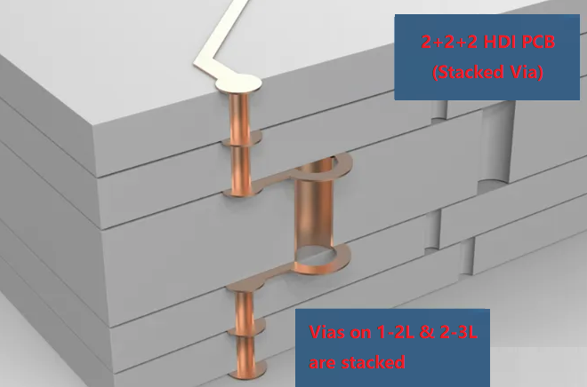
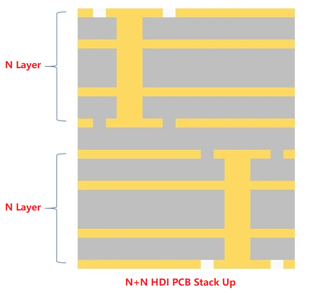
- Sequential build-up (1+N+1, 2+N+2, 3+N+3, and so on)
- Fine line/space (e.g., 75 µm/75 µm or better)
- Via-in-pad for BGA breakout
Modern ICs such as high pin-count BGAs, fine-pitch QFNs, and SiP modules simply cannot be routed on old-style 1-via-per-pin layouts. HDI PCB structures shorten critical paths, reduce via stubs, and keep return paths tight.
Key advantages of hdi pcb in modern designs include:
- Smaller board size with the same or higher function density
- Better signal integrity for multi-gigabit links
- Improved power distribution with dense stitching vias
- Room for mechanical design freedom in slim devices
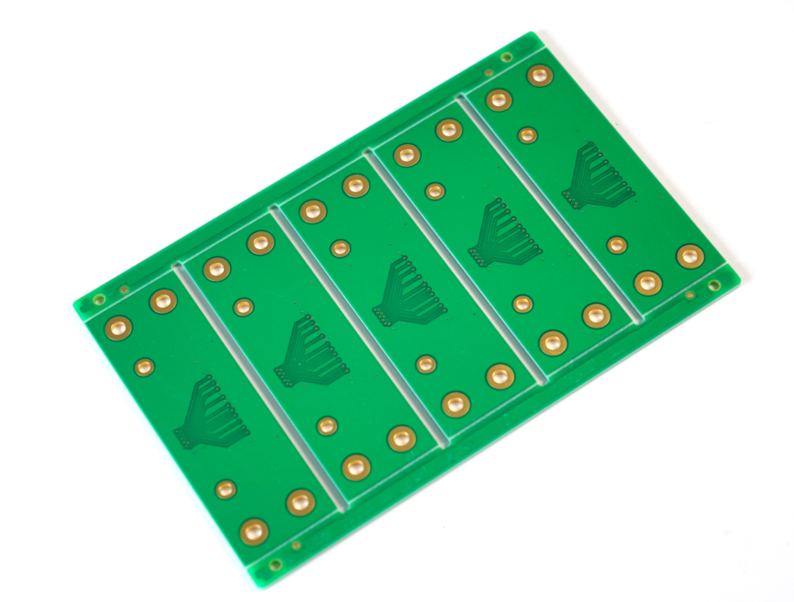
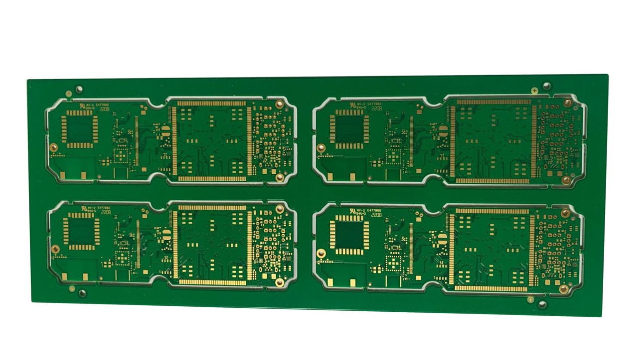
Because of this, HDI PCB technology is common in smartphones, tablets, communication modules, automotive radar, and compact industrial controllers.
What Is a High Tg PCB and How Does It Improve Reliability?
A high tg pcb uses laminate with a higher glass transition temperature than standard FR4. Tg is the point where the resin system changes from glassy to rubbery. Above this point, mechanical properties weaken quickly.
In a high Tg PCB, the Tg value might be 170–180°C or higher, instead of around 130–140°C for common materials. This increased Tg gives several benefits:
- Better dimensional stability during lead-free reflow
- Lower risk of pad lifting, delamination, or barrel cracks
- Reduced mechanical stress during temperature cycling
- Improved long-term reliability in high-temperature service
High Tg PCB materials also tend to have better thermal endurance over time, which helps in automotive under-hood zones, power supplies, motor drives, and LED lighting. They can handle more thermal stress without visible or hidden damage.
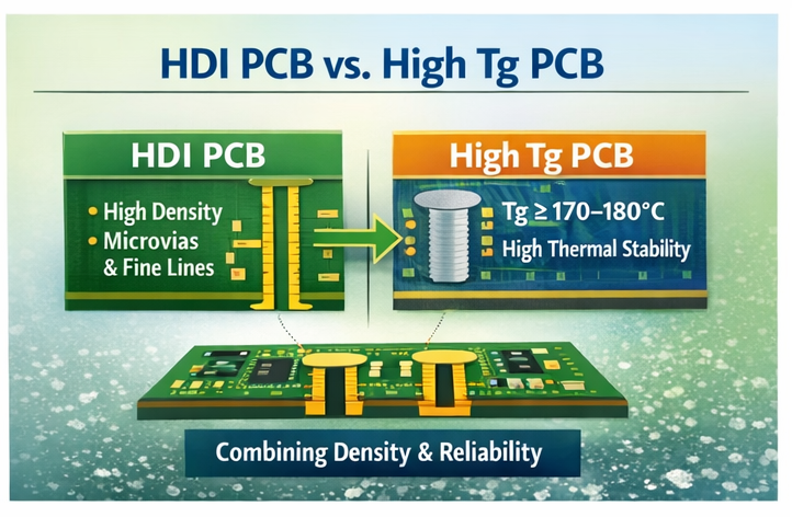
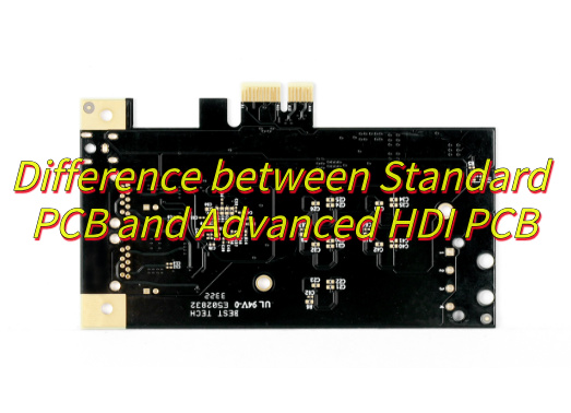
Differences Between HDI PCB and High Tg PCB
HDI and high Tg describe two different aspects of a PCB: one structural, one material. They often coexist, but they are not the same.
| Aspect | HDI PCB | High Tg PCB |
| Main focus | Interconnect density and routing | Thermal and mechanical stability |
| Key features | Microvias, fine lines, via-in-pad | Tg ≥ 170–180°C, better thermal endurance |
| Typical driver | Fine-pitch BGAs, compact form factor | Lead-free reflow, high operating temperature |
| Impact on layout | Strong effect on routing and stack-up | Moderate; affects stack-up and DFM margin |
| Impact on reliability | Better signal and via performance | Lower risk of warpage and delamination |
| Cost drivers | Laser drilling, lamination cycles, yield | Material price, process window, lamination setup |
An HDI PCB can use standard Tg material when the thermal profile is mild. A high Tg PCB can have no HDI features at all if density remains low. When the project pushes both limits, you combine them.
When Should HDI PCB and High Tg PCB Be Combined?
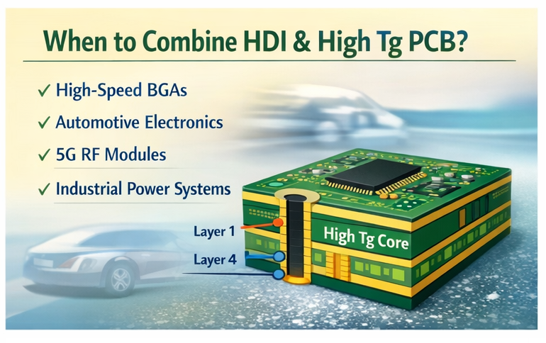
Combining HDI PCB and high Tg PCB makes sense when a design faces both density and thermal stress at the same time. Typical cases include:
- High-speed compute boards with large BGAs and multiple reflow passes
- Automotive radar or camera modules near engines or outdoor zones
- 5G RF front-ends in compact housings with limited airflow
- Industrial motion control or power electronics running at elevated temperature
You should consider an HDI & high Tg PCB solution if:
- The layout requires microvias or sequential lamination to escape key components
- The assembly line uses lead-free profiles with high peak temperature
- The product will see frequent on-off cycling or wide ambient temperature swings
- Field reliability and long service life carry high business value
In these scenarios, HDI brings routing freedom and signal quality, while high Tg materials protect the board structure against thermal and mechanical stress.
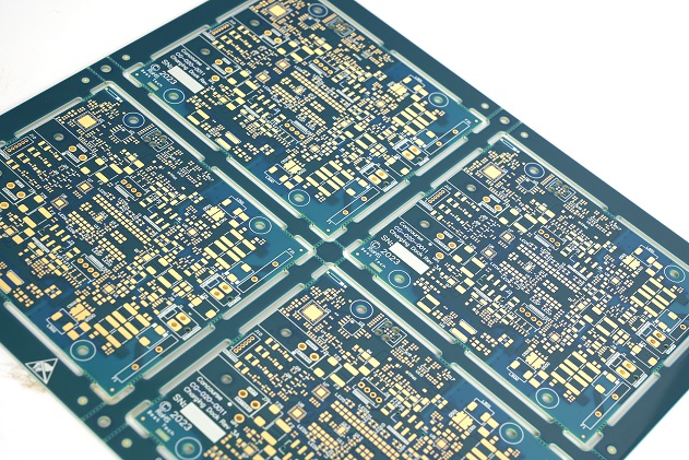
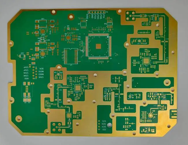
HDI & High Tg PCB Applications
HDI & high Tg PCB solutions appear in many sectors. Some typical applications are:
- Automotive electronics: ADAS, camera modules, radar, infotainment, EV control units
- Telecom and networking: 5G small cells, base stations, high-speed backplanes
- Industrial control: PLCs, servo drives, motion controllers, sensor hubs
- Medical devices: Imaging equipment, patient monitoring, compact diagnostic tools
- Consumer and wearable devices: Smartphones, tablets, smartwatches, AR/VR devices
All these products share common requirements: compact size, strict reliability targets, and long-term stability under shifting loads. HDI PCB structures handle fine-pitch and high-speed paths, while high Tg PCB materials carry the thermal and mechanical burden.
What Are the Key Design Considerations for HDI & High Tg PCB?
Designing HDI & high Tg PCB solutions is not just about choosing a material with higher Tg and shrinking traces. It needs careful coordination between layout, stack-up, and process limits. Key points include:
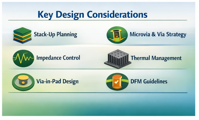
1. Stack-up planning early
Decide the HDI level (1+N+1, 2+N+2, etc.), copper thickness, and layer count early. Include high Tg material data, Dk/Df values, and lamination constraints in the first draft.
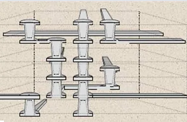
2. Microvia and buried via strategy
Keep microvia aspect ratios within the fabricator’s safe range. Use staggered rather than stacked microvias when reliability priority is high, unless the project can support enhanced filling processes.
3. Impedance control with high-speed pairs
High-density routing often pushes traces close together. Work with the fabricator to set precise trace width and spacing for each impedance class, considering the actual dielectric constant of the high Tg material.
4. Thermal management and copper balance
High Tg PCB materials support higher temperature, but heat still needs paths. Balance copper areas across the panel to reduce warpage. Provide solid ground planes, thermal vias, and clear heat paths.
5. Solder mask and via-in-pad design
When using via-in-pad on HDI pads, confirm filling and capping processes. Poorly filled vias can trap flux or reduce solder joint strength.
6. Design for manufacturability (DFM)
Follow the manufacturer’s design rules for minimum line/space, annular ring, drill size, and pad shapes. Good DFM work reduces scrap and supports stable quality.
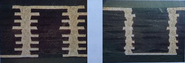
What Manufacturing Challenges Exist in HDI & High Tg PCB?
Manufacturing HDI PCB involves several engineering challenges because the process pushes the limits of micro-fabrication, interlayer reliability, material control, and inspection accuracy. Each stage demands strict tolerance management to keep performance stable in high-density layouts.
- Microvia and blind-via drilling accuracy is difficult because HDI requires via diameters
below 0.15 mm. Laser drilling must stay stable and precise to avoid rough walls, incomplete holes, or weak plating that may cause electrical issues in stacked via structures.
- Layer-to-layer registration and lamination control demand micron-level alignment.
High-order HDI needs multiple lamination cycles, and any shift in imaging, resin flow, or pressure can create opens, shorts, or signal loss.
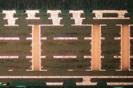
- Fine-line etching becomes harder as line width and spacing drop to 3 mil or less. Thin
traces are sensitive to under-etching or over-etching, and thicker copper (4–10 oz) makes precise control even more challenging.
- Plating and via filling must deliver uniform copper to keep interconnections stable.
Voids, trapped gas, or uneven filling weaken microvias and reduce long-term reliability, especially when the design needs high breakdown voltage.
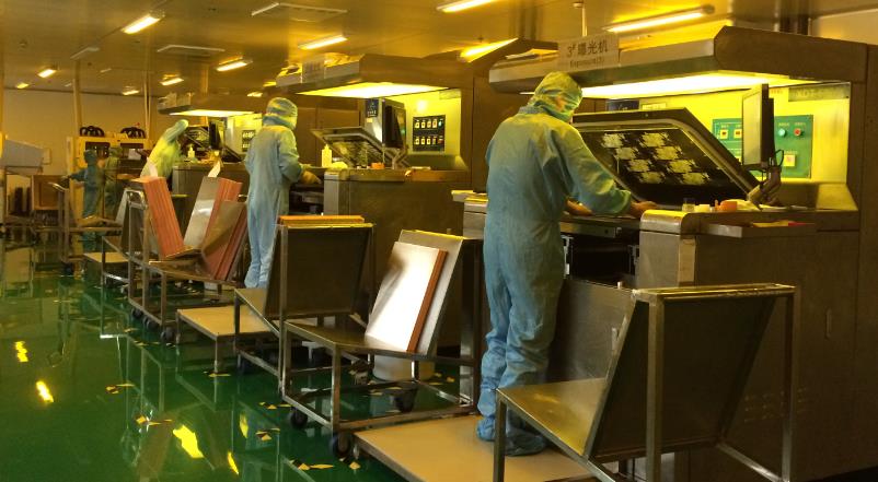
How EBest Circuit (Best Technology) Supports HDI & High Tg PCB Solutions?
EBest Circuit (Best Technology) supports HDI & High Tg PCB Solutions from early design review through mass production and assembly. Our team focuses on turning demanding ideas into stable, repeatable products.
- Engineering and DFM for HDI and high Tg
Our engineers review your stack-up, HDI level, and component layout at the start. We suggest suitable high Tg materials, via strategies, and impedance structures based on your performance and cost targets.
- HDI PCB manufacturing capability
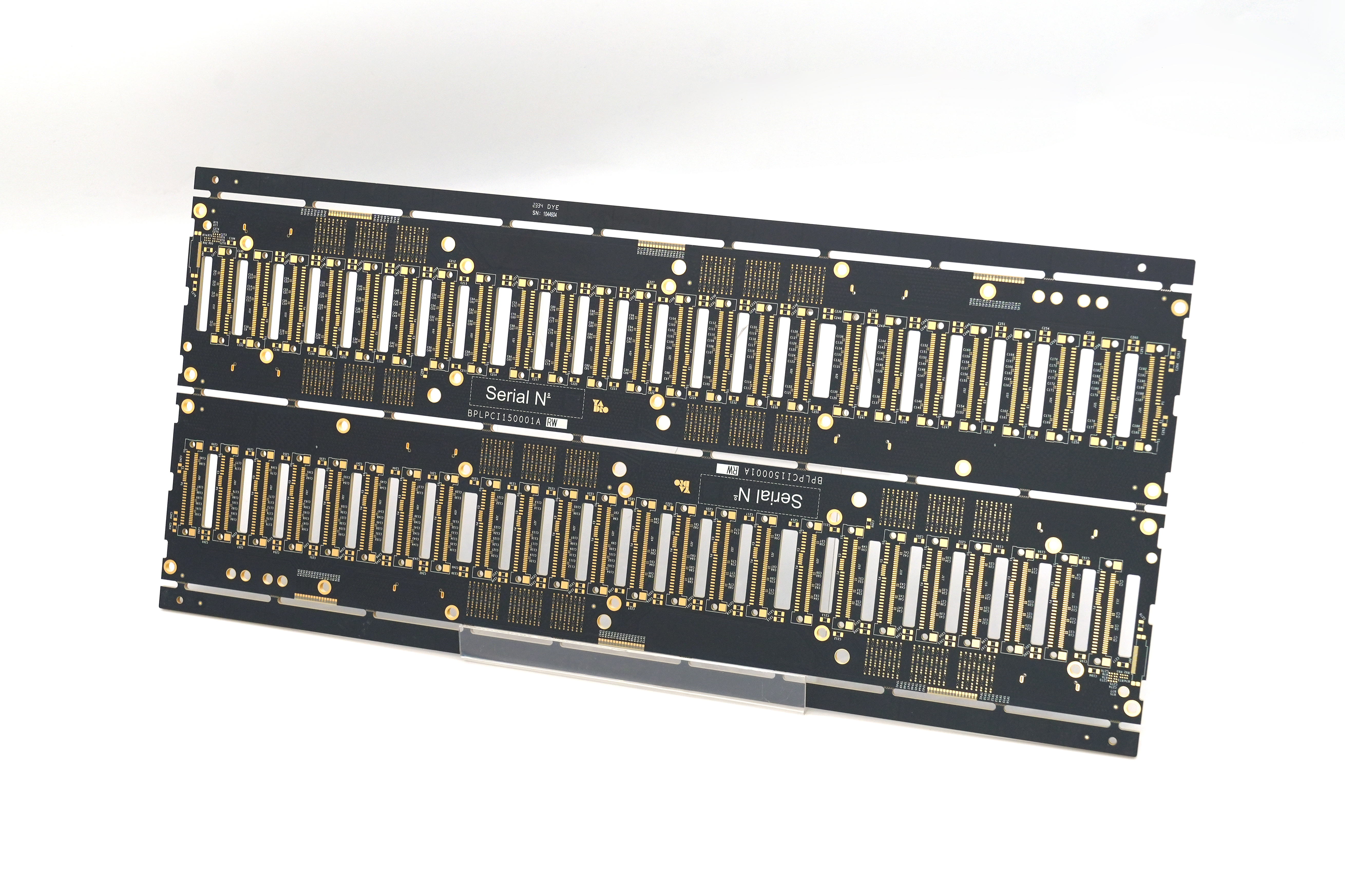
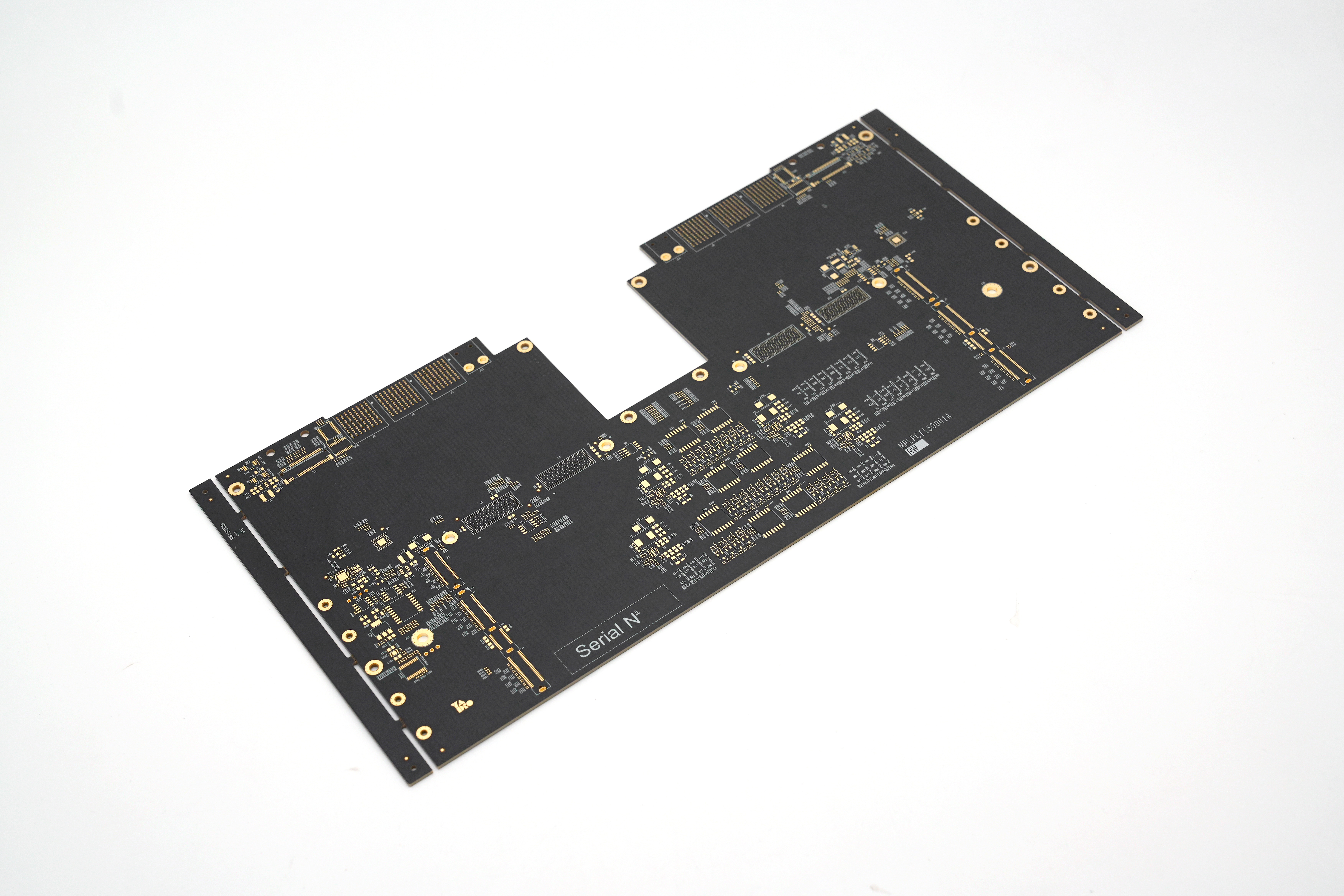
We support fine line and space routing, laser-drilled microvias, via-in-pad, and multi-step lamination. Typical HDI builds such as 1+N+1, 2+N+2, and higher structures can be handled with controlled registration and repeatable yields.
- High Tg and advanced materials
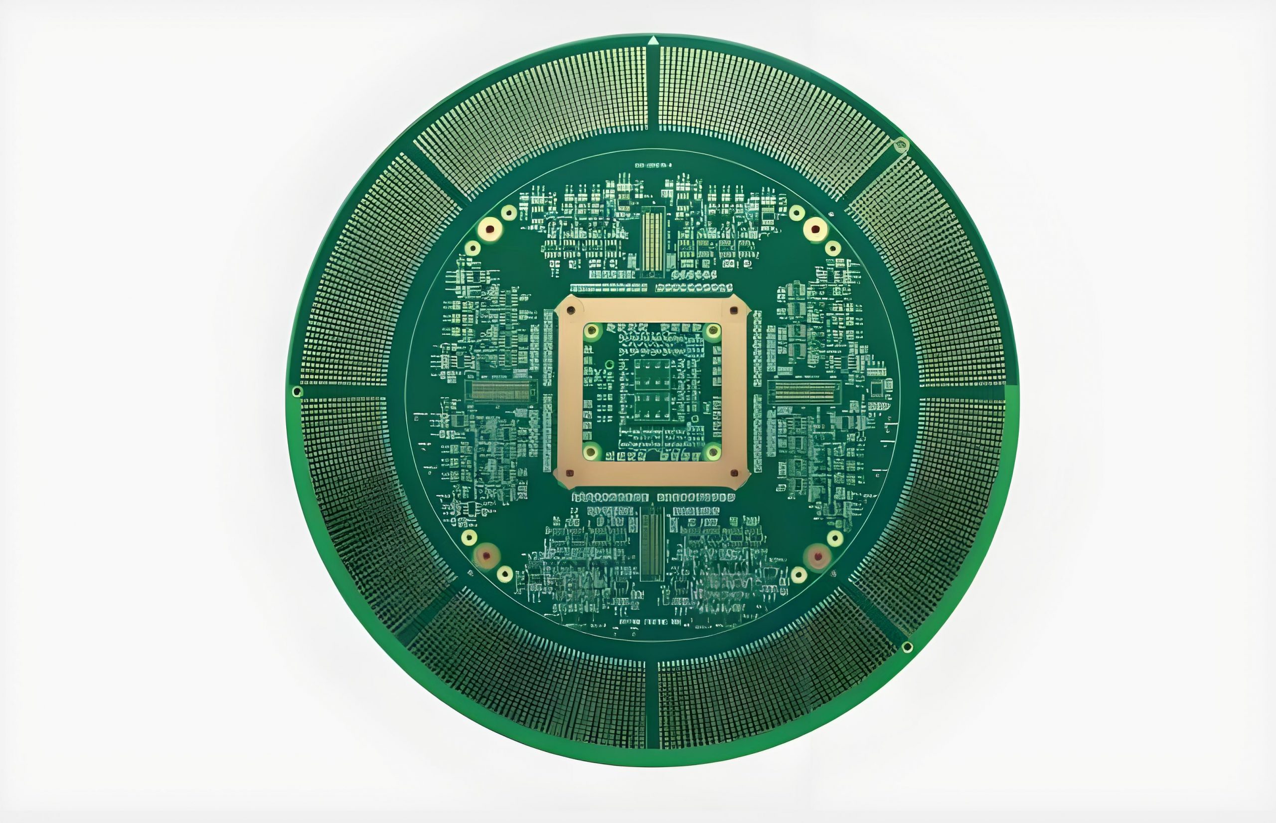
We work with well-known high Tg PCB laminates and can also support hybrid builds for projects that need both RF and digital performance. Material selection focuses on Tg, Td, Dk/Df, and reliability under your real reflow profile.
- PCBA assembly with process control
EBest Circuit (Best Technology) provides SMT and through-hole assembly for HDI and high Tg boards in both China and Vietnam. Lead-free profiles, X-ray for BGA, and AOI help keep quality stable for dense layouts.
- Quality systems and traceability
Our factories follow ISO9001, ISO13485 for medical, IATF16949 for automotive, and AS9100D for aerospace. We also run MES systems to track each lot from material incoming through final shipment. This supports clear traceability and faster root-cause analysis if any issue appears.
For buyers who need a long-term partner for HDI & high Tg PCB solutions, this combination of engineering support, HDI process capability, and certified quality systems reduces risk and saves internal effort.
FAQs about HDI & High Tg PCB Solutions
1. Is HDI PCB always more expensive than a standard multilayer board?
HDI PCB usually costs more per panel due to laser drilling, extra lamination, and tighter controls. However, the total product cost can drop because the board is smaller, the BOM can be simplified, and performance improves.
2. When do I really need a high Tg PCB instead of normal FR4?
You should consider a high Tg PCB when your design uses lead-free solder, has more than one reflow cycle, or runs in high ambient temperatures. Automotive, power, and industrial products are common cases where high Tg material significantly improves reliability.
3. Can I use HDI without high Tg material for consumer products?
Yes. Many consumer devices use hdi pcb structures on mid-range Tg materials because their operating temperature is moderate and lifetime targets are shorter. The decision depends on your thermal profile and reliability goals.
4. Are stacked microvias less reliable than staggered ones?
Stacked microvias can be reliable when the process is well controlled, but they need stricter plating and filling quality. For very harsh environments, many designers still prefer staggered microvias for extra margin, unless dense routing forces stacking.
5. How early should I involve EBest Circuit (Best Technology) in an HDI & high Tg PCB project?
The best time is before you freeze the stack-up and routing strategy. Early DFM and material discussion help avoid later redesign, reduce risk, and shorten the path from prototype to stable mass production.
If you are planning a new design that needs smaller size, higher speed, and stronger thermal performance, HDI & High Tg PCB Solutions may be the right direction. You can share your Gerber files, stack-up ideas, or even just a concept, and EBest Circuit (Best Technology) will help you evaluate practical options, costs, and timelines for your next project.