PCB manufacturing PCB manufacturing
Home > Blog

Fast PCB Prototyping

Bluetooth Headset PCB Manufacturer | Fast Flex PCB Prototyping
Friday, April 3rd, 2026

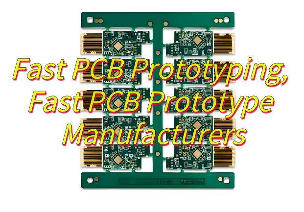
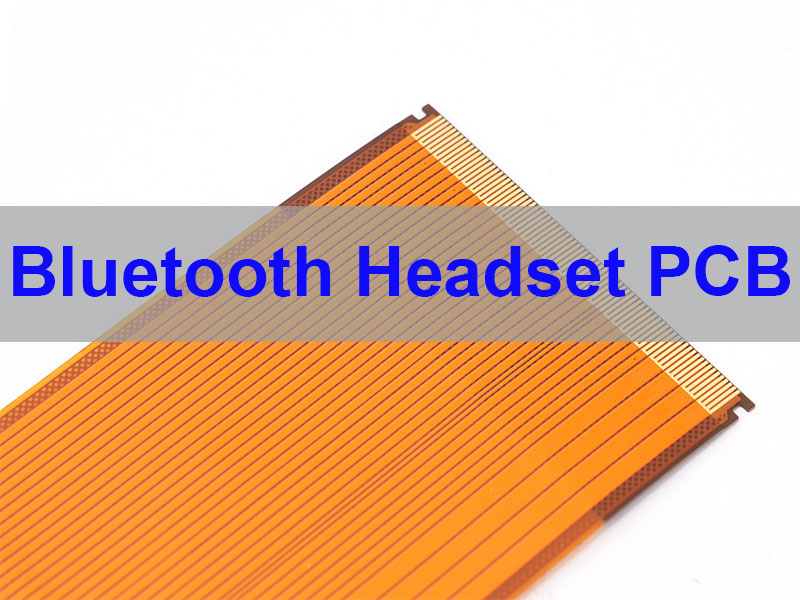
A Bluetooth headset PCB is a compact printed circuit board that integrates wireless communication, audio processing, power management, and peripheral control circuits to enable stable Bluetooth connectivity and high-quality sound transmission in headset devices. This blog delves into the critical role of Bluetooth headset PCBs, exploring design considerations, manufacturing challenges, and how to choose the right partner for fast, reliable prototyping and production.

What are the most common pain points when developing a Bluetooth headset PCB?
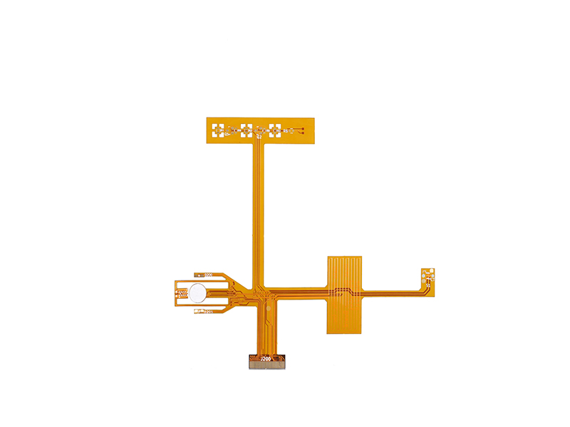
  • Design Complexity:​ Integrating RF (Bluetooth), audio codec, power management, and often flexible circuits into a tiny form factor is overwhelmingly complex.
  • Slow Prototyping Cycles:​ Lengthy lead times for PCB prototypes delay testing, iteration, and ultimately, your time-to-market.
  • Component Sourcing Hassles:​ Procuring genuine, miniaturized components (like 01005 packages) and dealing with supply chain instability.
  • Assembly Precision Challenges:​ Achieving flawless soldering on high-density, rigid-flex designs with fine-pitch components (e.g., 0.25mm BGA).
  • Reliability & Compliance Anxiety:​ Ensuring the final product is durable, delivers consistent audio quality, and meets necessary quality and safety standards.

The solution lies in partnering with a manufacturer that transforms these challenges into streamlined processes.

  • Expert ODM Design Support:​ Leverage a team that provides end-to-end design services, optimizing your schematic and layout for performance, manufacturability, and cost.
  • Accelerated Prototyping Pipeline:​ Access services that guarantee quick-turn FPC prototyping, with the capability to deliver initial samples within days, not weeks.
  • Reliable Supply Chain Access:​ Benefit from established partnerships with authorized distributors (e.g., Digikey, Mouser) to source authentic components and manage your BOM effectively.
  • High-Precision Assembly Lines:​ Utilize state-of-the-art SMT lines equipped with advanced printers, SPI, and precision placers capable of handling 01005 components to ensure flawless PCBA.
  • Rigorous Quality Assurance:​ Implement a full suite of inspections (AOI, X-Ray, functional testing) adhering to IPC standards, guaranteeing the reliability and performance of every board.

At EBest Circuit (Best Technology), we are a specialized flexible PCB and PCBA manufacturer with 20 years of experience. We bridge the gap between complex design and reliable mass production. Our one-stop service covers everything from FPC/rigid-flex design and rapid prototyping to component procurement and turnkey PCBA assembly. With a 3,000㎡ factory equipped with advanced machinery like Yamaha SMT lines and comprehensive testing equipment, we are built to handle your project from the initial quote for flex PCB​ prototypes to full-scale production. Pls feel free to contact our team anytime at sales@bestpcbs.com for a consultation.

 Bluetooth Headset PCB

Key Considerations for Bluetooth Headset PCB Design

Designing the PCB for a Bluetooth headset is a multidisciplinary challenge. It requires a harmonious balance between RF performance, audio fidelity, power efficiency, and mechanical constraints, especially when using flexible circuits to fit ergonomic forms.

  • RF Layout Optimization:​ The Bluetooth antenna and RF trace layout are paramount. Impedance must be tightly controlled (typically 50Ω), and the RF section needs isolation from digital noise sources to ensure stable connectivity and range.
  • Audio Signal Integrity:​ Separate analog and digital ground planes, use proper filtering, and shield audio lines to minimize noise, crosstalk, and distortion for clear sound output.
  • Power Management Design:​ Implement efficient DC-DC converters and LDOs to minimize quiescent current drain. Careful PCB layout for the battery management system (BMS) is crucial for safety and longevity.
  • Miniaturization Strategies:​ Employing HDI (High-Density Interconnect) techniques, micro-vias, and finer trace/space (down to 3/3mil) is often necessary to shrink the board size without sacrificing functionality.
  • Thermal Management:​ Even in small devices, heat from the Bluetooth SoC or audio amplifier must be dissipated via thermal vias and careful copper pours to prevent throttling or discomfort.
  • Mechanical Durability:​ For designs incorporating flexible circuits, bend radius, stiffener placement (using PI or FR4), and material selection (Polyimide) must be engineered to withstand repeated flexing during use.

In summary, a successful Bluetooth headset PCB design is a feat of integration, demanding expertise in RF, analog, digital, and mechanical domains to create a reliable, high-performance, and compact board.

 Bluetooth Headset PCB

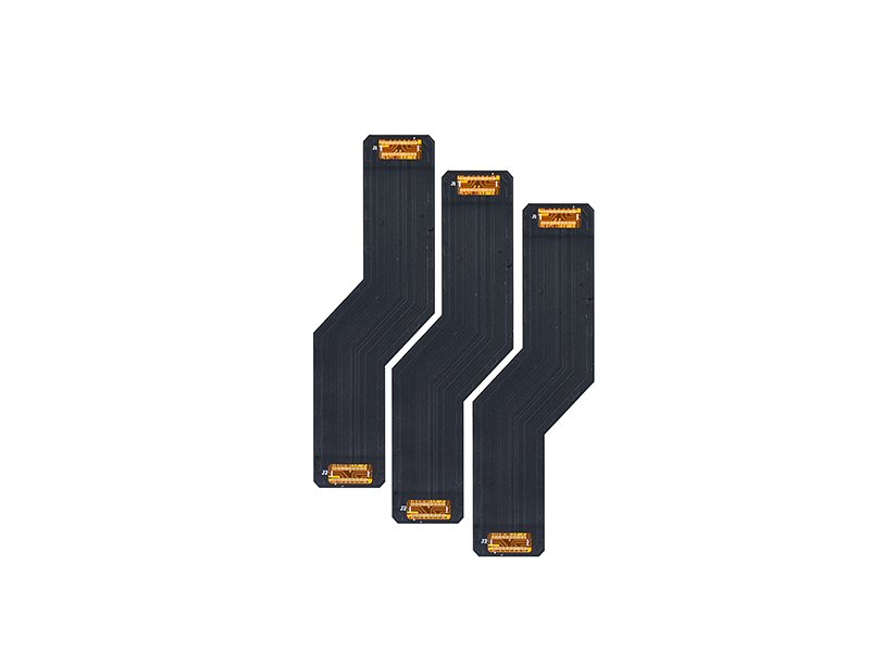
Material Selection for Flexible PCBs in Headsets

The choice of materials directly impacts the performance, durability, and cost of the bluetooth headset PCB. Flexible circuits enable the sleek, comfortable designs modern users expect.

  • Base Substrate:​ Polyimide (PI) is the industry standard (e.g., DuPont’s Kapton), offering excellent thermal stability (>500°C), chemical resistance, and flexibility. Polyester (PET) is a lower-cost alternative for less demanding applications.
  • Copper Foil:​ Rolled annealed copper is preferred for dynamic flex applications due to its superior fatigue resistance. Thickness options range from 1/3 OZ (12µm) to 2 OZ (70µm) to balance current carrying capacity and flexibility.
  • Coverlay/Stiffener:​ Photo-imageable coverlay or polyimide film protects the circuits. Strategic stiffeners (made of PI, FR4, or even stainless steel) are added at connector areas or where components are mounted to provide rigidity for soldering.
  • Adhesives:​ Acrylic or epoxy-based adhesives bond layers. Adhesiveless constructions (e.g., 2-layer FCCL) offer better thermal performance and thinner, more reliable profiles for high-end applications.
  • Surface Finish:​ Choices like ENIG (Electroless Nickel Immersion Gold) provide a flat, solderable, and wire-bondable surface. Hard gold is used for edge connectors (gold fingers) that withstand repeated insertion wear.

The table below summarizes common flexible PCB material capabilities relevant to headset manufacturing:

ParameterPolyimide (PI)PET
Laminate Thickness0.025 / 0.050 / 0.125 / 0.175 mm0.025 / 0.050 / 0.075 mm
Copper Foil0.012, 0.018, 0.035, 0.070 mm0.035, 0.070 mm
Min Trace/Space0.075 mm (3 mil)0.075 mm (3 mil)
Solder Heat Resistance280°C for 10 secs280°C for 10 secs

Selecting the right material stack-up is a critical decision that influences the board’s electrical performance, bend life, and overall reliability in the final product.

Fast-Turn Prototyping and Assembly Process

Speed is critical in the fast-paced consumer electronics market. A streamlined prototyping and assembly process allows for rapid iteration and validation of your bluetooth speaker headset PCB module.

  1. Design Review & DFM Analysis:Our engineers perform a thorough design for manufacturability (DFM) check upon receiving your Gerber files, identifying potential issues before production begins.
  2. Rapid Fabrication:Leveraging in-house manufacturing of flexible, rigid-flex, and FR4 PCBs, we can produce prototype boards quickly. For standard FR4 prototypes, lead times can be as fast as 24 hours for 1-2 layer boards.
  3. Component Kitting:For turnkey projects, we source all components from authorized distributors. Every part undergoes incoming inspection to verify authenticity and specification against the BOM.
  4. Precision Assembly:The process follows strict IPC standards:
    • Solder Paste Printing:​ Using laser-cut stencils and 3D SPI (Solder Paste Inspection) to ensure precise deposition.
    • Component Placement:​ High-speed chip shooters and precision placers accurately mount components, down to 01005 size.
    • Reflow Soldering:​ A controlled, nitrogen-inerted reflow profile ensures perfect solder joints.
    • Through-Hole Assembly:​ For any THT components, selective or wave soldering is employed.
  5. Comprehensive Testing:Every assembled board goes through AOI (Automated Optical Inspection) and X-Ray inspection (for BGA). Functional testing validates the Bluetooth pairing, audio playback, and all key features.

This integrated, quality-focused process ensures that you receive fully functional, reliable PCBA prototypes in the shortest possible timeframe, accelerating your development cycle.

Quality Control and Testing Standards

Quality cannot be an afterthought. For a bluetooth headset PCB, rigorous testing is essential to ensure audio clarity, connection stability, and long-term user satisfaction.

  • In-Process Inspection (IPQC):​ Quality checks are embedded at every stage—from raw material (copper clad laminate) inspection to etching, lamination, and plating processes.
  • Automated Optical Inspection (AOI):​ 2D and 3D AOI machines scan the assembled board to detect soldering defects, component misplacement, or missing parts.
  • X-Ray Inspection:​ Critical for examining hidden solder joints under BGA, QFN, or inside rigid-flex constructions, ensuring there are no voids or bridges.
  • Flying Probe & Electrical Test:​ Verifies circuit connectivity (open/short) and basic electrical functionality of the bare PCB and the final assembly.
  • Functional Testing (FCT):​ The most critical step. Custom test jigs and software simulate real-world operation—testing Bluetooth connectivity range, audio input/output quality, battery charging, button response, and firmware performance.
  • Reliability Testing:​ Depending on requirements, boards may undergo stress testing like thermal cycling, bend testing for flex circuits, and drop testing to validate durability.

We adhere to international quality management systems (ISO 9001:2015, ISO 13485:2016) and IPC standards, building quality into the process rather than just inspecting it out at the end. This systematic approach is what delivers the reliable bluetooth speaker headset PCB module​ that your product deserves.

Cost Optimization Strategies

While quality is paramount, managing costs is essential for maintaining product viability. Smart decisions during the design and manufacturing phases can significantly optimize the cost of your bluetooth headset PCB.

  • Design for Cost (DFC):​ Work with your manufacturer’s engineers early. Simplifying the layer count, standardizing hole sizes, and optimizing the panel layout to maximize yield can lead to substantial savings.
  • Material Selection Balance:​ Choose material grades and copper weights that meet but do not exceed the electrical and mechanical requirements. For instance, using 1/2 OZ copper instead of 1 OZ where current allows reduces cost.
  • Standardize Processes:​ Where possible, opt for standard surface finishes (like ENIG over ENEPIG), common drill sizes, and standard solder mask colors to avoid special process charges.
  • Panelization Efficiency:​ Designing your board in a shape that nests efficiently with others on a production panel minimizes material waste. Our engineers can advise on the most efficient panelization strategy.
  • Volume Forecasting:​ While prototyping costs are higher per unit, providing realistic volume forecasts allows the manufacturer to plan material procurement and production scheduling for better long-term pricing.
  • Component Alternatives:​ For long-lead or expensive components, our sourcing team can suggest form-fit-function alternatives that maintain performance at a lower cost.

Effective cost optimization is a collaborative effort between your design team and a manufacturing partner with deep supply chain knowledge and production expertise.

Applications and Use Cases for Bluetooth Headset PCBs

Bluetooth headset PCBs are widely used across consumer and professional audio devices.

Typical applications include:

  • True Wireless Stereo (TWS) earbuds
  • Over-ear wireless headphones
  • Sports and waterproof headsets
  • Gaming headsets with low-latency requirements
  • Call center and business communication headsets

Each application has different priorities, such as battery life, RF stability, or mechanical durability.

How to Choose a Reliable Bluetooth Headset PCB Manufacturer?

Selecting the right manufacturer directly impacts product quality, cost, and delivery time.

Key evaluation criteria:

  • RF PCB experience (Bluetooth, WiFi, antenna design support)
  • Flex PCB manufacturing capability (fine pitch, thin materials)
  • PCBA integration (one-stop service reduces lead time)
  • Testing capability (RF + functional test support)
  • Supply chain stability (authorized component sourcing)
  • Certifications (ISO, IPC standards compliance)

A reliable partner should also provide:

  • Free DFM feedback
  • Engineering support during design phase
  • Transparent communication and fast response
 Bluetooth Headset PCB

Overall, bluetooth headset PCB​ is the unsung hero that determines the performance, reliability, and user experience of modern wireless audio devices. This article has explored the critical aspects of its design, material selection, fast prototyping, stringent quality control, and cost management.

With 20 years of dedicated experience in flexible and rigid-flex PCB manufacturing, a full turnkey PCBA assembly service, and a commitment to rapid prototyping, EBest Circuit (Best Technology) is equipped to guide your project from concept to mass production efficiently and reliably. Ready to discuss your Bluetooth headset project? Pls feel free to contact us at sales@bestpcbs.com for a quote or consultation.

FAQs About Bluetooth Headset PCB

1. What type of PCB is used in Bluetooth headsets?
Most designs use a combination of rigid PCB and flexible PCB (rigid-flex or FPC).

2. How many layers are typical for headset PCBs?
Usually 2–4 layers, depending on RF and power complexity.

3. Why is impedance control important?
It ensures stable RF signal transmission and minimizes signal loss.

4. Can you support low-volume prototyping?
Yes, small batch production is commonly supported for product validation.

5. What is the typical turnaround time?
PCB prototypes can be completed in 3–7 days, with PCBA in about 1–2 weeks.

Fast PCB Prototyping, Fast PCB Prototype Manufacturers
Friday, June 6th, 2025

Need fast PCB prototyping solutions? Fast PCB Prototyping enables quick hardware testing through rapid manufacturing, requiring careful vendor choice, thermal optimization, signal testing, and quality checks to ensure 24-hour delivery with reliable performance.

EBest Circuit (Best Technology) stands out as a premier fast PCB prototype manufacturer by delivering industry-leading 24-hour turnaround times without compromising quality. Our automated smart factories equipped with advanced 6-layer simultaneous drilling technology and high-speed automated SMT production lines enable rapid prototyping cycles that are 40% faster than industry standards. We maintain this speed while achieving 99.8% first-pass yield through precision SMT placement systems and real-time thermal monitoring. For mission-critical projects, our express service guarantees functional prototypes within 24 hours, supported by 24/7 engineering support and live production tracking. Clients benefit from our decade of expertise in high-speed digital and RF designs, with specialized solutions for HDI, flex-rigid, and high-frequency boards up to 77GHz. Our ISO 9001-certified quality system combines automated optical inspection (AOI), flying probe testing, and signal integrity verification to ensure reliability at accelerated production speeds. The integration of cutting-edge SMT assembly infrastructure, optimized logistics networks, and dedicated quick-turn production lines makes us the preferred partner for startups requiring rapid iteration capabilities. Welcome to contact us: sales@bestpcbs.com.

What Is Fast PCB Prototyping?

Fast PCB Prototyping is the process of rapidly manufacturing functional printed circuit board samples for testing and validation before mass production. It enables hardware developers to quickly verify designs, identify potential issues, and accelerate product development cycles. Leading Fast PCB Prototype Manufacturers specialize in delivering high-quality prototypes within 24-72 hours using advanced manufacturing techniques and strict quality control. This service is particularly valuable for international trade clients who need to maintain competitive timelines while ensuring reliability. By partnering with trusted fast PCB prototyping providers, businesses can reduce development costs, speed up market entry, and minimize risks in electronics manufacturing.

Fast PCB Prototyping

What Are Benefits of Fast PCB Prototyping?

Benefits of fast PCB prototyping:

  • Speed to Market‌ – Fast PCB Prototyping cuts waiting time from weeks to 1-3 days, helping global clients meet tight deadlines and stay ahead of competitors.
  • Cost Savings‌ – Early design validation through fast PCB prototyping prevents expensive rework in mass production, reducing overall project costs.
  • Risk Reduction‌ – Leading fast PCB prototype manufacturers test functionality before full-scale production, minimizing defects and supply chain delays.
  • Flexible Iterations‌ – Quick turnaround allows multiple design revisions, ensuring optimal performance before finalizing orders.
  • Quality Assurance‌ – Reputable manufacturers use advanced equipment (e.g., 6-layer HDI) and ISO-certified processes for reliable prototypes.
  • Global Logistics Support‌ – Many fast PCB prototype manufacturers offer DHL/FedEx shipping, ensuring timely delivery for overseas clients.
  • Scalability‌ – Seamless transition from prototypes to bulk production with the same supplier avoids compatibility issues.
  • Technical Collaboration‌ – Expert engineers from top manufacturers provide design feedback to enhance product durability and efficiency.

What Are Applications of Fast PCB Prototyping?

Application of Fast PCB prototyping:

Consumer Electronics Acceleration‌

  • Smartphone motherboard prototypes (10-16 layers) for 5G antenna array testing within 72 hours.
  • Wearable device flexible circuits (0.1-0.3mm thickness) with 3-day iterative cycles.
  • VR headset PCBs for thermal dissipation validation using 2oz copper prototypes.

Automotive Electronics Validation‌

  • EV battery management systems (6-8 layer prototypes) for crash simulation in 5 working days.
  • Autonomous vehicle radar modules (77GHz RF boards) with impedance control (±3%).
  • Dashboard display rigid-flex boards tested under -40°C to 105°C temperature cycles.

Medical Device Compliance‌

  • Portable ECG monitors with medical-grade FR4 material certification in 48 hours.
  • Implantable device prototypes featuring biocompatible gold plating (0.05μm).
  • Surgical robot PCBs with 20μm laser micro-vias for high-density interconnects.

Industrial Automation Solutions‌

  • Motor drive controllers (10oz heavy copper) for vibration testing within 96 hours.
  • PLC interface cards with 0.15mm trace/space for harsh environment validation.
  • Machine vision camera boards supporting 10Gbps data transmission testing.

Aerospace & Defense Systems‌

  • Satellite communication boards (RT/duroid 5880 material) for space environment simulation.
  • Avionics prototypes undergoing 6-week accelerated aging tests equivalent to 5 years.
  • UAV flight controllers with conformal coating options for moisture resistance.

Telecommunications Infrastructure‌

  • 5G mm Wave antenna arrays (32-layer stack-ups) for signal integrity analysis.
  • Optical network equipment with ≤1dB insertion loss prototypes.
  • Base station power modules supporting 1000W/cm² thermal stress tests.
Fast PCB Prototyping

How to Choose Fast PCB Prototype Manufacturers?

Below are tips about how to choose fast PCB prototype manufacturer:

Technical Expertise

  • Look for manufacturers with HDI, flex-rigid, and RF/microwave PCB prototyping experience.
  • A U.S. client chose a partner with LDI technology to achieve 25μm traces for a wearable EEG device.

Certifications

  • Must-Haves include ISO 9001, ISO 13485, AS9100, and UL 94V-0.
  • Ensure compliance with EU’s RoHS/REACH, China’s CQC, and Japan’s PSE.

Turnaround Time

  • Aim for 24–72 hours for 2-layer PCBs, 5–7 days for 8+ layers.
  • Avoid factories promising “24-hour turnaround” without clarifying complexity limits.

Material Inventory

  • Check if they stock high-TG FR4, Rogers 4350B, and IMS for immediate use.
  • A German firm lost 2 weeks when a manufacturer had to import PTFE for a 5G antenna prototype.

DFM Support

  • Top manufacturers offer free DFM reviews to catch issues like trace spacing violations.
  • A Canadian startup reduced rework by 60% after a DFM audit flagged solder mask alignment errors.

Quality Control

  • Look for AOI, X-ray for BGAs, and TDR for impedance control.
  • Ask for ITAF 16949 or IPC-6012 Class 3 compliance.

Cost Transparency

  • Request a breakdown for setup, engineering, and NRE fees.

 Scalability

  • Ensure the factory handles both 5-piece prototypes and 100K-unit runs.
  • A Japanese EV firm cut lead times by 40% by using the same partner for BMS prototypes and mass production.

Communication & Support

  • Choose partners with English/Spanish/Mandarin-speaking engineers.
  • Look for cloud portals with Gerber viewers, order tracking, and instant chat.

Customer Reviews & Case Studies

  • Check platforms like Trustpilot or LinkedIn for reviews from foreign clients.
  • Avoid factories with multiple complaints about missed deadlines or quality lapses.
Fast PCB Prototype Manufacturers

How to Optimize Thermal Management Fast PCB Prototype Design?

Below are strategies to optimize thermal management fast PCB prototype design:

Material Selection for Thermal Conductivity

  • Base Materials: Use high-Tg FR-4 (≥170°C) or ceramic-filled laminates (e.g., Rogers TMM) for improved heat dissipation.
  • Copper Weight: Opt for 2oz+ copper thickness to reduce resistance and lower Joule heating.

Component Placement Optimization

  • Thermal Zoning: Isolate heat-generating components (e.g., MOSFETs, FPGAs) from temperature-sensitive parts (e.g., oscillators, ADCs).
  • Airflow Alignment: Orient heat sinks and fans parallel to natural convection currents.

 Thermal Via Arrays

  • Design: Deploy 0.3mm-diameter vias in 5×5 grids under hot components to conduct heat to inner layers or ground planes.
  • Spacing: Maintain ≤1mm pitch between vias for optimal thermal conductivity.

Embedded Heat Spreaders

  • Integration: Embed copper or aluminum plates (1–2mm thick) within the PCB stack-up for direct heat sinking.
  • Example: Reduced junction temperature by 15°C in a 100W LED driver prototype.

Plane Resistance Minimization

  • Layer Stackup: Allocate dedicated power/ground planes adjacent to heat-generating layers.
  • Thickness: Use 2oz copper for power planes to lower DC resistance (<2mΩ/sq).

Thermal Interface Materials (TIMs)

  • Selection: Apply phase-change materials (e.g., 3W/mK) or graphite sheets for low-thermal-impedance interfaces.
  • Application: Use stencils to ensure 100µm±10µm thickness consistency.

Forced Convection Integration

  • Fan Placement: Position blowers near high-power components with static pressure ratings matching enclosure airflow resistance.
  • Ventilation: Include 8mm+ diameter holes in PCB cutouts for unobstructed airflow.

Monte Carlo Thermal Simulation

  • Tool: Use ANSYS Icepak or SimScale to model transient temperature rise under worst-case loads.
  • Validation: Compare simulations with IR camera measurements (e.g., FLIR E76) post-assembly.

Dynamic Power Management

  • Firmware: Implement thermal throttling in microcontrollers to reduce clock speeds by 20–40% at Tj > 105°C.
  • Sensors: Integrate NTC thermistors near hotspots for real-time monitoring.

Post-Production Thermal Cycling

  • Stress Test: Subject prototypes to 100+ cycles (-40°C to +125°C) to identify solder joint fatigue.
  • Rework: Use hot air rework stations (e.g., 480°C nozzle) for localized BGA reflow without delamination.

How to Achieve Fast PCB Prototyping Within 24 Hours?

Below are 10 practical steps to accelerate turnaround times without compromising quality:

1. Design Simplification

  • Layer Reduction: Limit to 2–4 layers for faster etching and drilling.
  • Standard Footprints: Use pre-verified component libraries to avoid DFM rework.

2. Automated DFM Checks

  • Tool: Integrate KiCad DRC or Altium Design Rules to flag errors like trace spacing violations or missing solder mask layers.
  • Example: A 30-minute DFM audit reduced rework by 50% in a 4-layer PCB prototype.

3. Material Pre-staging

  • Stockpile: Maintain inventory of common substrates (e.g., FR-4 1.6mm, 1oz copper) and stencils for SMT assembly.
  • Pre-Cut Panels: Use 18×24-inch panels to minimize waste and speed up CNC routing.

4. Parallel Manufacturing

  • Simultaneous Operations:
    • Layer 1: Etching + drilling.
    • Layer 2: Solder mask application.
    • Layer 3: Surface finish (e.g., ENIG).
  • Tool: Use multi-spindle CNC machines to drill 1,000+ holes/minute.

5. High-Speed SMT Assembly

  • Pick-and-Place: Deploy 8-head SMT machines with 15,000 CPH (Components Per Hour) throughput.
  • Reflow Optimization: Use nitrogen-inerted ovens for 3-minute lead-free soldering cycles.

6. Skip-Lot Testing

  • Sampling: Test 1 board from every 10-unit batch for impedance/SI, assuming consistent process controls.
  • Risk Mitigation: Reserve 100% testing for mission-critical designs (e.g., medical, aerospace).

7. Express Logistics

  • Local Couriers: Partner with same-day delivery services for component sourcing within a 50-mile radius.
  • Air Freight: Use priority shipping for out-of-stock items (e.g., Rogers 4350B laminates).

8. Real-Time Production Tracking

  • Dashboard: Implement IoT sensors to monitor etching baths, oven temperatures, and SMT head pressures.
  • Alerts: Receive SMS/email notifications for deviations (e.g., reflow oven exceeding 245°C).

9. 24/7 Engineering Support

  • On-Call Team: Rotate shifts to handle design queries, DFM reviews, and test failures.
  • Live Chat: Use tools like Slack or Microsoft Teams for instant communication.

10. Pre-Certification Preparation

  • Documentation: Pre-fill FCC/CE test reports using simulated data to expedite compliance.
  • Labeling: Print UL marks and RoHS symbols during solder mask application.

How to Ensure Quality of Fast PCB Prototype Manufacturing?

Below are steps to guarantee reliability, compliance, and performance:

Design for Manufacturability (DFM) Reviews

  • Proactive Checks: Use professional EDA tools (e.g., Altium, Cadence) to validate designs for line width/spacing, impedance control, and drill hole ratios.
  • Example: A U.S. client reduced rework by 40% after a DFM audit flagged improper solder mask clearance on a 12-layer PCB.

 Material Certification & Traceability

  • Supplier Audits: Require ISO 9001/IATF 16949-certified suppliers for base materials (e.g., FR-4, Rogers 4350B) and track batch consistency via COAs (Certificates of Analysis).
  • Red Flag: Avoid suppliers lacking UL 94V-0 or RoHS compliance documentation.

Advanced Process Control

  • Critical Parameters: Monitor etching time/temperature (±2°C accuracy), laser drilling precision (≤25μm tolerance), and copper plating thickness (1–2oz standard).
  • Tool: Implement SPC (Statistical Process Control) to detect deviations in real time.

Automated Optical Inspection (AOI)

  • Defect Detection: Use AOI to identify solder bridges, missing pads, or over-etching with 99.95% accuracy.
  • Integration: Pair with ICT (In-Circuit Testing) for comprehensive electrical validation.

X-ray Inspection for Hidden Defects

  • BGA/QFN Analysis: Deploy X-ray to detect voids, misalignments, or insufficient solder in ball grid arrays.
  • Case Study: A Japanese firm avoided a 15% failure rate in automotive ECUs by catching cold solder joints via X-ray.

Environmental Stress Testing

  • Thermal Cycling: Subject prototypes to -55°C to +125°C cycles (1,000+ cycles for automotive/aerospace grade).
  • Humidity Resistance: Test at 85°C/85% RH for 168 hours to simulate tropical conditions.

Signal Integrity Verification

  • TDR/TDT Testing: Validate impedance control (±5% tolerance) and crosstalk mitigation on high-speed designs (e.g., 10Gbps+).
  • Tool: Use Keysight E5071C or similar analyzers for precise measurements.

Supplier Collaboration & Audits

  • Qualification: Prioritize manufacturers with IPC-6012 Class 3, AS9100, or ISO 13485 certifications.
  • On-Site Audits: Inspect facilities for ESD control (≤100V static discharge) and 5S compliance.

First Article Inspection (FAI)

  • Documentation: Require FAI reports detailing layer stack-up, via plating thickness, and surface finish (e.g., ENIG, OSP).
  • Example: A German client rejected a batch due to 0.5mm deviation in impedance vs. 50Ω specified in the FAI.

Post-Production Analytics

  • Failure Analysis: Use SEM (Scanning Electron Microscopy) for root-cause diagnosis of delamination or micro-cracks.
  • Data-Driven Adjustments: Apply machine learning to predict and prevent recurring defects.
Fast PCB Prototype Manufacturing

How to Test Signal Integrity of Fast Turn Prototype PCB Board?

Testing signal integrity (SI) in fast-turn PCB prototypes is critical to ensure high-speed designs meet performance targets. Below are 10 detailed, actionable steps to validate SI, combining advanced tools, industry standards, and real-world examples:

1. Pre-Test Design Review

  • Validate Specifications: Confirm impedance requirements (e.g., 50Ω for USB 3.2, 100Ω for PCIe), transmission line lengths (≤5cm for 28Gbps signals), and differential pair coupling (≥3W rule).
  • Simulation: Use tools like Hyper Lynx to simulate reflections, crosstalk, and attenuation before prototyping.
  • Example: A U.S. client identified a 12% impedance mismatch in a 16-layer PCB by simulating layer transitions pre-production.

2. Time Domain Reflectometry (TDR) Testing

Tool: Use a Tektronix TDR/TDT Analyzer to measure impedance continuity.

Process:

  • Probe critical nets (e.g., DDR5 DQ lines, HDMI traces).
  • Check for discontinuities like via stubs, neck-downs, or solder mask bridges.

Threshold: Target ±5% impedance tolerance (e.g., 47.5–52.5Ω for 50Ω trace).

3. Eye Diagram Analysis

  • Tool: Generate eye diagrams using a Keysight DSOX1204G Oscilloscope and BERT (Bit Error Rate Tester).
  • Metrics:
  • Eye Height: ≥600mV for 5Gbps signals.
  • Eye Width: ≥0.4 UI (Unit Interval) for low jitter.
  • Case Study: A Japanese firm reduced eye closure by 30% by optimizing pre-emphasis in a 10Gbps SERDES link.

4. Crosstalk Measurement

Test Setup: Inject a 1GHz sine wave into aggressor traces while monitoring victim traces.

Limits:

  • Near-End Crosstalk (NEXT): ≤3% of aggressor signal.
  • Far-End Crosstalk (FEXT): ≤1.5% for 28Gbps+ signals.

Mitigation: Increase spacing to ≥3x trace width or use grounded guard traces.

5. Insertion Loss (S21) & Return Loss (S11) Testing

Tool: Use a Vector Network Analyzer (VNA) (e.g., Copper Mountain Technologies M5065).

Thresholds:

  • Insertion Loss: <-3dB at Nyquist frequency (e.g., <14GHz for 28Gbps PAM4).
  • Return Loss: <-20dB at target frequencies.

Red Flag: A German client rejected a PCB batch due to -8dB insertion loss at 12GHz, traced to poor FR-4 material selection.

6. Power Integrity Co-Testing

PDN (Power Delivery Network) Analysis:

  • Measure DC IR drop (<2% of nominal voltage) using a Keysight N6705C Power Analyzer.
  • Check AC impedance (<10mΩ at 100kHz–1MHz) with a Picotest J2120A Injector.

Example: A Canadian startup reduced voltage ripple by 40% by adding decoupling capacitors near a 12V-to-1.8V LDO.

7. Thermal Stress Testing

Process:

  • Subject PCB to 1,000 thermal cycles (-55°C to +125°C).
  • Monitor SI degradation using TDR/eye diagrams post-cycling.

Impact: A Japanese automotive client found a 15% increase in insertion loss in a PCB lacking ENIG finish after thermal shock.

8. Automated SI Validation

  • Tools: Use LabVIEW or Python scripts to automate TDR sweeps and eye diagram captures.
  • Benefit: Reduce testing time by 60% and eliminate manual errors.
  • Integration: Pair with JTAG Boundary Scan for concurrent functional testing.

9. Compliance Verification

  • Standards: Ensure compliance with:
  • IPC-6012: For impedance control and via reliability.
  • IEEE 802.3: For Ethernet PHY performance.
  • USB-IF: For USB 4.0 Gen 3×2 (20Gbps) compliance.
  • Certification: Use authorized labs like Granite River Labs (GRL) for final validation.

10. Iterative Design Optimization

  • Debug Workflow:
  • Isolate failing nets using near-field probes.
  • Adjust trace length matching (≤10mil skew for DDR5) or replace materials.
  • Case Study: A U.S. client resolved 20% eye closure in a 400Gbps QSFP-DD module by optimizing back drilling depth.

Conclusion
In conclusion, fast PCB prototyping accelerates product launches, reduces costs, and ensures global compliance. From consumer electronics to aerospace, its applications drive innovation. Choose EBest Circuit (Best Technology) for 24-hour turnaround, ISO-certified quality, and advanced SI/thermal management. Expert in HDI, flex-rigid, and RF/microwave PCBs, we guarantee performance. Contact EBest Circuit (Best Technology) now for a quote and elevate your prototyping efficiency: sales@bestpcbs.com.