What is copper multilayer PCB? Let’s discover its material, benefits, applications, design guide for wearable device, production process through this blog.
Are you troubled with these problems?
- High-frequency signal degradation killing your design?
- Heat dissipation always a bottleneck?
- Yield rates dropping with layer stacking?
EBest Circuit (Best Technology) can provide service and solutions:
- Rapid Response – 24/7 engineering support, samples delivered in 48 hours.
- Cost Efficiency – Intelligent panelization + material reuse cuts costs by 15%.
- Transparency – Real-time production tracking with photo verification at key stages.
Welcome to contact us if you have any inquiry for copper multilayer PCB: sales@bestpcbs.com.
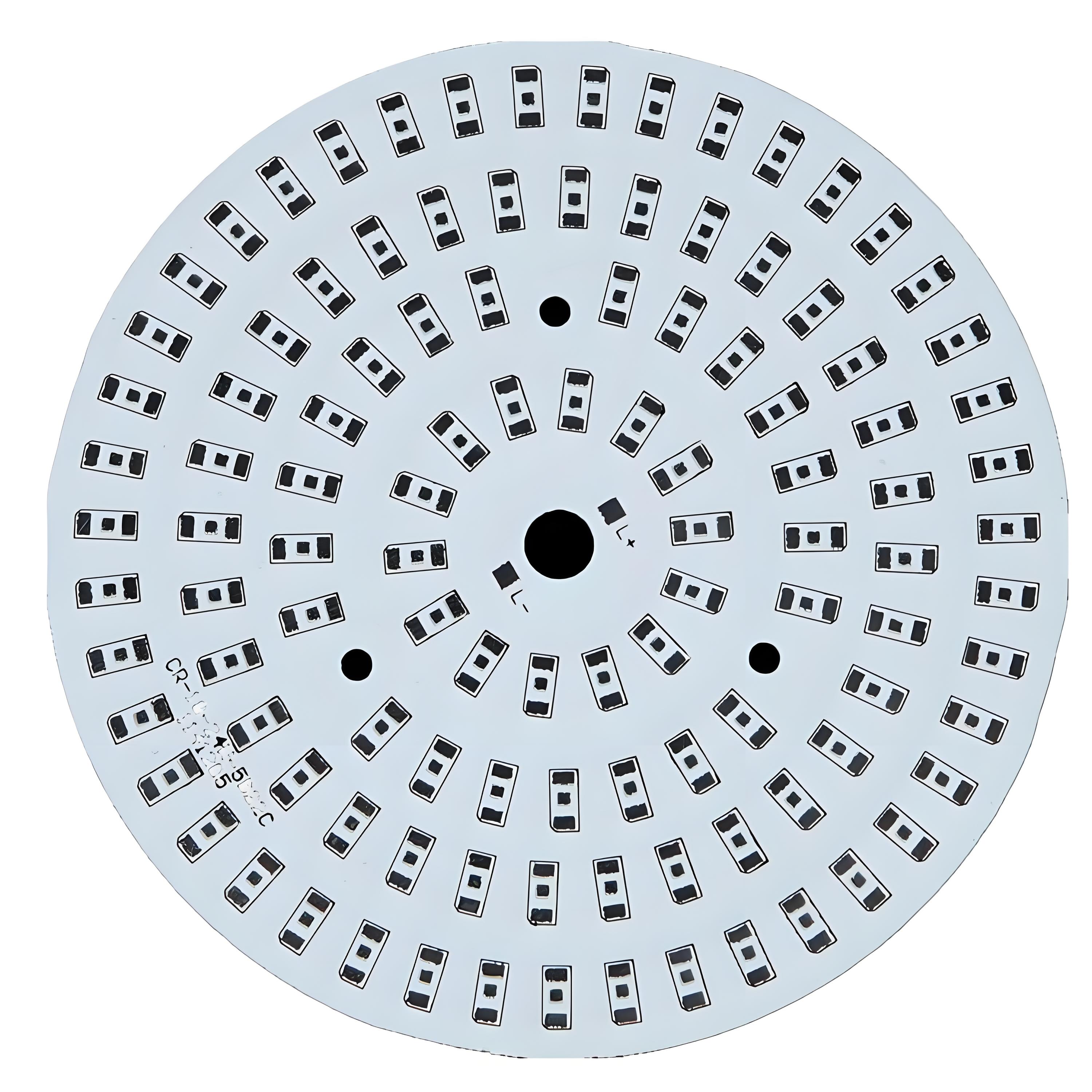
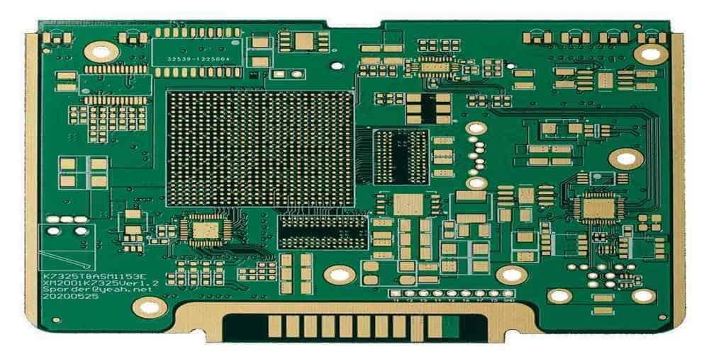
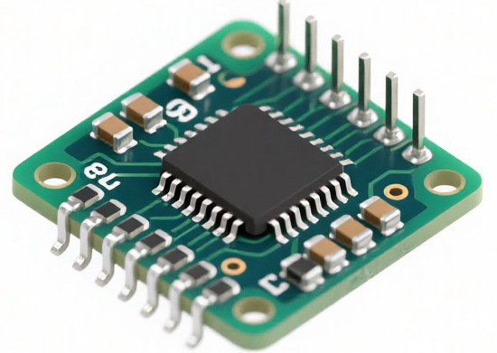
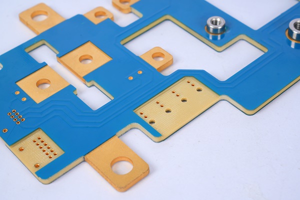
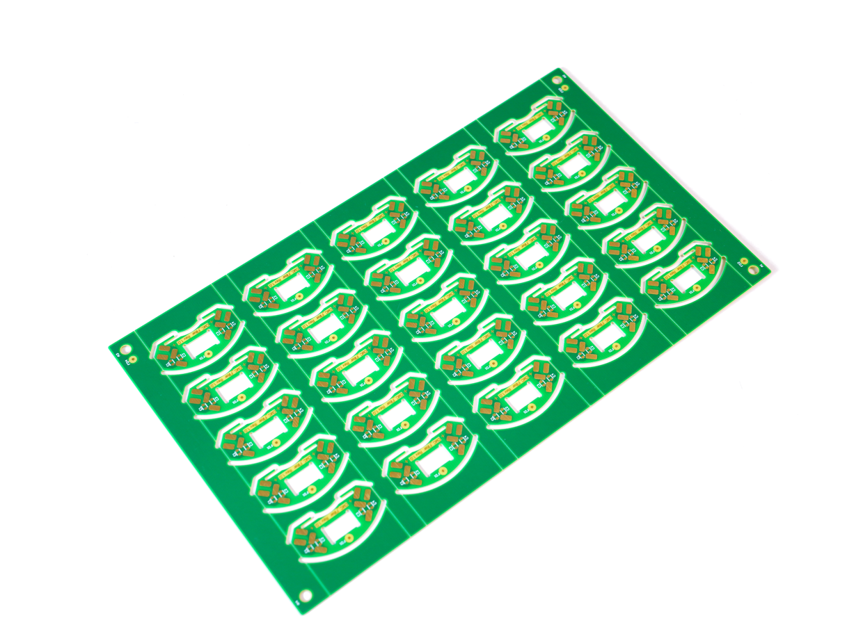
What is Copper Multilayer PCB?
Copper Multilayer PCB consist of alternating copper conductive layers and insulating materials (such as FR-4 or polyimide) bonded together through a lamination process. Copper’s high thermal conductivity (386W/m·K) and electrical conductivity support complex circuit designs, enabling high-density interconnection between layers through through-holes, blind vias, or buried vias.
This type of PCB is suitable for high-power applications (such as automotive electronics and 5G base stations), offering superior heat dissipation and signal stability compared to single- or double-layer PCBs. Its symmetrical structure (e.g., copper-prepreg-core-prepreg-copper) enhances mechanical strength and controls impedance. Some models also utilize thermal isolation technology to directly conduct heat.
What is Material of Multilayer Copper PCB?
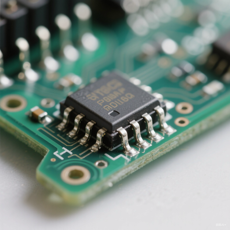
1. Conductive Layer
- Composition: Electrolytic copper foil (ED) or rolled copper foil (RA)
- Features: Thickness 0.5–6 oz/ft² (17–210 μm), conductivity ≥58 MS/m (20°C), surface finish available: brown oxide (OSP) or nickel-gold (ENIG).
2. Insulation
- FR-4: Epoxy resin + fiberglass, dielectric constant 4.2–4.8 (1 GHz), heat resistance 130°C (standard) / 170°C (high Tg).
- Polyimide (PI): Dielectric constant 3.4–3.6 (1 GHz), heat resistance >250°C, short-term temperature resistance ≥300°C.
3. Prepreg (PP)
- Composition: 7628/2116/1080 glass cloth impregnated with epoxy resin
- Features: Thickness 0.05–0.2mm (0.1–0.4mm after lamination), resin content 52%–65%, curing conditions 180°C/60min.
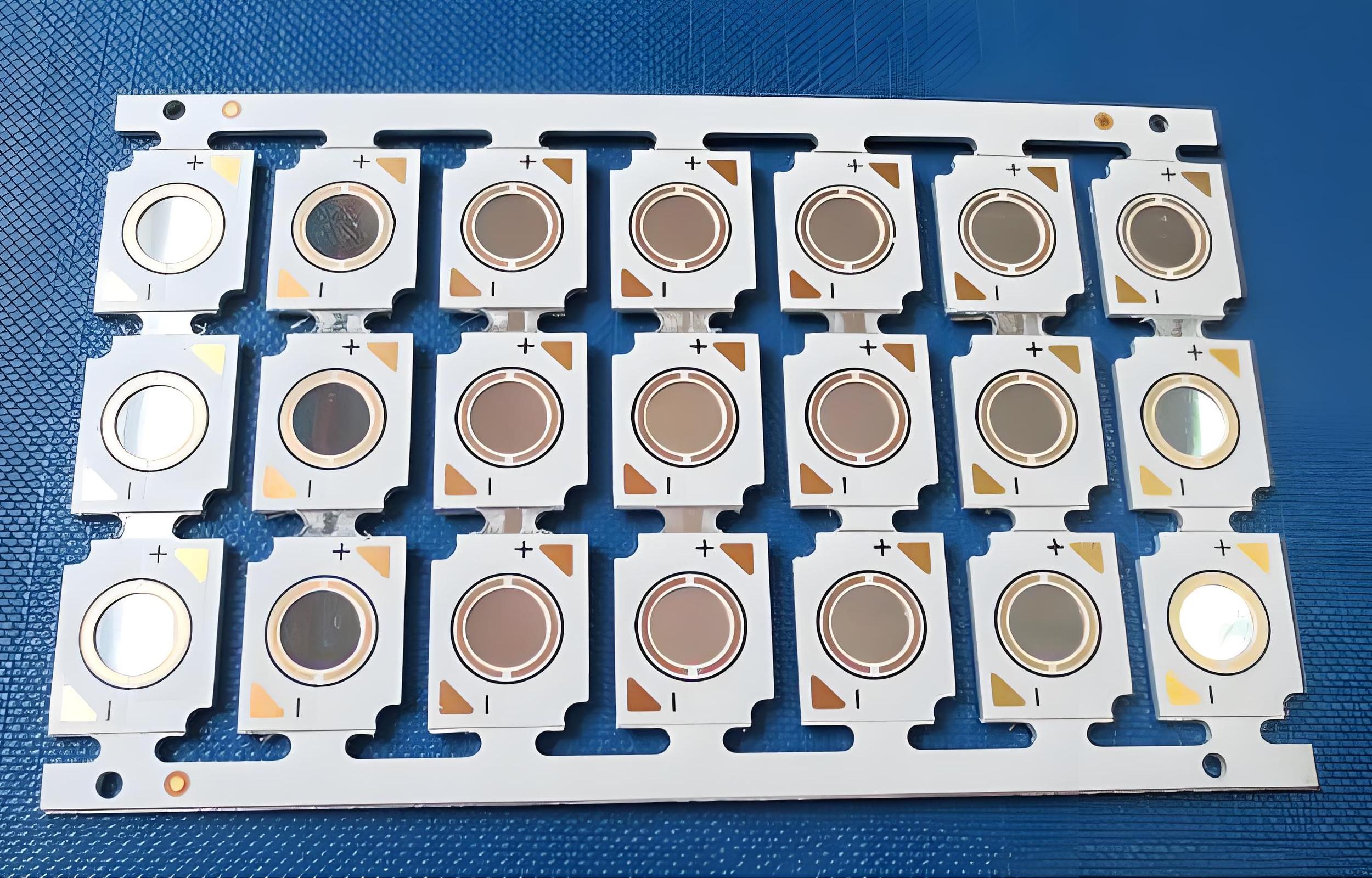
4. Metal Substrate (Optional)
- Aluminum Substrate: 1050/6061 alloy, thermal conductivity 180–220 W/m·K, thickness 1.0–3.2mm.
- Copper Substrate: Electrolytic copper, thermal conductivity 386 W/m·K, thickness 0.5–2.0mm.
5. High-Frequency Material (Optional)
- PTFE: Polytetrafluoroethylene, dielectric constant 2.2–2.5 (10 GHz), dissipation factor <0.001 (10 GHz).
- Rogers RO4003C: dielectric constant 3.38 (10 GHz), dissipation factor 0.0027 (10 GHz).
6. Solder Mask
- Composition: Liquid Photosensitive Solder Mask Ink (LPI)
- Characteristics: Thickness 10–25μm, Temperature Resistance ≥ 150°C (short-term), Insulation Resistance ≥ 1×10⁸Ω.
What Are Advantages of Copper Multilayer PCBs?
Benefits of copper multilayer PCB:
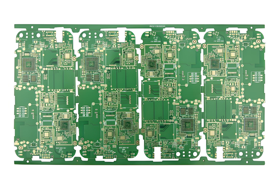
- High-density integration capabilities: By stacking multiple conductive layers (up to 32 layers), complex circuits can be integrated within a limited space, meeting the demands of miniaturized devices such as smartphone motherboards.
- Excellent heat dissipation performance: Copper foil has a thermal conductivity of 400. W/m·K (nearly twice that of aluminum substrates), combined with a thick copper design (3–10 oz), allows for rapid heat conduction and reduces the junction temperature of high-power devices.
- High-frequency signal integrity: Specialized high-frequency materials (such as PTFE) have a dielectric constant as low as 2.2–3.5, reducing signal loss and making them suitable for 5G base stations and radar systems.
- Optimized electromagnetic compatibility: Multi-layer ground and power planes effectively shield electromagnetic interference (EMI) and reduce crosstalk risks.
- Improved mechanical strength: Copper substrates offer superior deformation resistance to traditional FR-4, making them suitable for vibration environments such as automotive electronics.
- Current carrying capacity: Thick copper layers (6 oz+) support high current transmission and reduce voltage drop in power modules.
- Design flexibility: Supports advanced processes such as blind and buried vias and mixed dielectric layers to meet the needs of high-frequency, high-speed, and high-power hybrid designs.
- Long-term reliability: Copper’s oxidation resistance and multi-layer laminate structure (using prepreg PP) extend product life, making them suitable for industrial control equipment.
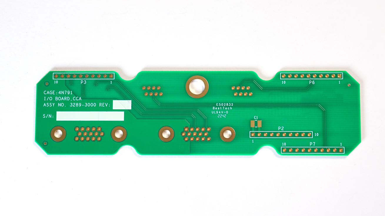
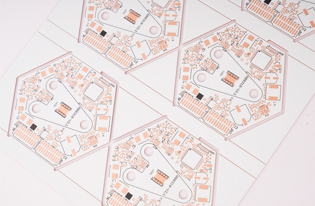
What Are Applications of Copper Multilayer PCB?
- Communications Equipment: 5G base stations, routers, mobile phone signal repeaters, fiber optic receivers
- Computers and Data Centers: Server motherboards, hard drive controllers, graphics cards, storage devices
- Medical Equipment: Heart monitors, CT scanners, X-ray equipment
- Industrial Control and Automotive Electronics: Motor controllers, industrial automation systems, power converters, in-vehicle electronics
- Aerospace: Satellite systems, space exploration equipment, radar
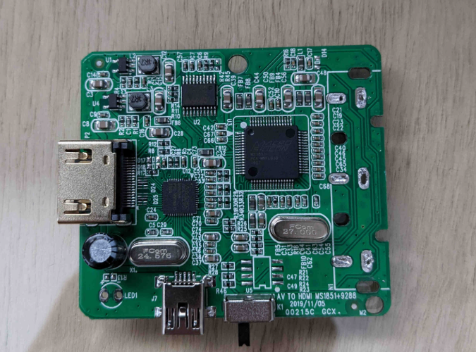
- Consumer Electronics: Smartphones, wearable devices, game consoles
- Energy and Power Systems: Power amplifiers, battery chargers, rectifiers, high-power conversion devices
How to Design a Copper Multilayer PCB for Wearable Device?
1. Material Selection & Substrate Optimization
- Substrate: Prioritize polyimide (PI) or liquid crystal polymer (LCP), thickness 0.05–0.1mm, for flexibility (bending radius <5mm) and high-temperature resistance (Tg >250℃).
- Conductive Layer: Use ultra-thin rolled annealed copper foil (RA, 0.5oz/17μm) to balance flexibility and conductivity (conductivity ≥58 MS/m).
- Adhesive Layer: Apply low-modulus prepreg (PP) to reduce interlayer stress and prevent cracking during bending.
2. Stackup Design & Flexibility
- Layer Count: Prioritize for 4-layer boards (Signal-Ground-Power-Signal) with total thickness 0.4–0.6mm to minimize weight.
- Symmetry: Distribute copper layers symmetrically (e.g., Cu-PI-Cu) to avoid warping during bending; place ground and power planes adjacent to reduce EMI.
- Flexible Zones: Use coreless structures (copper foil + PI only) in bending areas (e.g., wristband connections) for unrestricted flexibility.
3. Signal Integrity Assurance
- High-Speed Signals: Design Bluetooth/Wi-Fi antennas as microstrip lines with 50Ω impedance control (trace width 0.15mm, spacing 0.1mm) and avoid 90° bends.
- Differential Pair Routing: Route high-speed interfaces (USB, MIPI) with equal length (tolerance ±5mil) and spacing ≥3x trace width to minimize crosstalk.
- Shielding: Add copper shielding layers (width ≥2mm) around antennas, grounded via stitching to reduce external EMI.
4. Power Distribution & Low-Power Design
- Layered Power: Implement split power planes (e.g., 1.8V/3.3V) with power-ground spacing 0.1mm and decoupling capacitors (10μF + 100nF).
- Low-Power Components: Select ultra-low-power MCUs (e.g., STM32L series) and PMICs, paired with hardware watchdogs to prevent lockups.
- Layout Optimization: Place batteries, PMICs, and MCUs close to minimize trace length and reduce static power consumption.
5. Thermal Management Strategies
- Heat Dissipation: Place copper foils (1oz thickness) under heat-generating components (MCUs, power chips) and connect via thermal vias (diameter 0.2mm, pitch 0.5mm) to external thermal areas.
- Thermal-Electric Separation: Isolate high-power LEDs or battery chargers with dedicated copper layers to prevent heat transfer to sensitive components.
- Material Enhancement: Embed graphene thermal films (0.01mm thickness) in critical zones to improve lateral heat conduction.
6. Mechanical Reliability & Bend Resistance
- Solder Mask: Use high-flexibility solder mask (e.g., Taiyo PSR-9000), thickness 10μm, rated for >100,000 bend cycles.
- Surface Finish: Apply ENIG (Electroless Nickel Immersion Gold) or OSP (Organic Solderability Preservative) to prevent copper oxidation and ensure solder reliability.
- Validation: Pass dynamic bend tests (radius 3mm, 1Hz frequency, 10,000 cycles) and accelerated aging (85℃/85%RH, 168 hours).
7. Electromagnetic Compatibility (EMC) & Compliance
- Grounding: Connect metal enclosures (e.g., wristband, buttons) to PCB ground via spring contacts or conductive adhesives, forming a Faraday cage to mitigate ESD.
- Certification: Achieve CE (EU) or FCC (US) EMC compliance, testing across 80MHz–6GHz to ensure stable operation in complex electromagnetic environments.
- Wireless Charging: Position Qi-standard coils at PCB edges, away from antennas and sensors to avoid interference.
How was Copper Multilayer PCB Made?
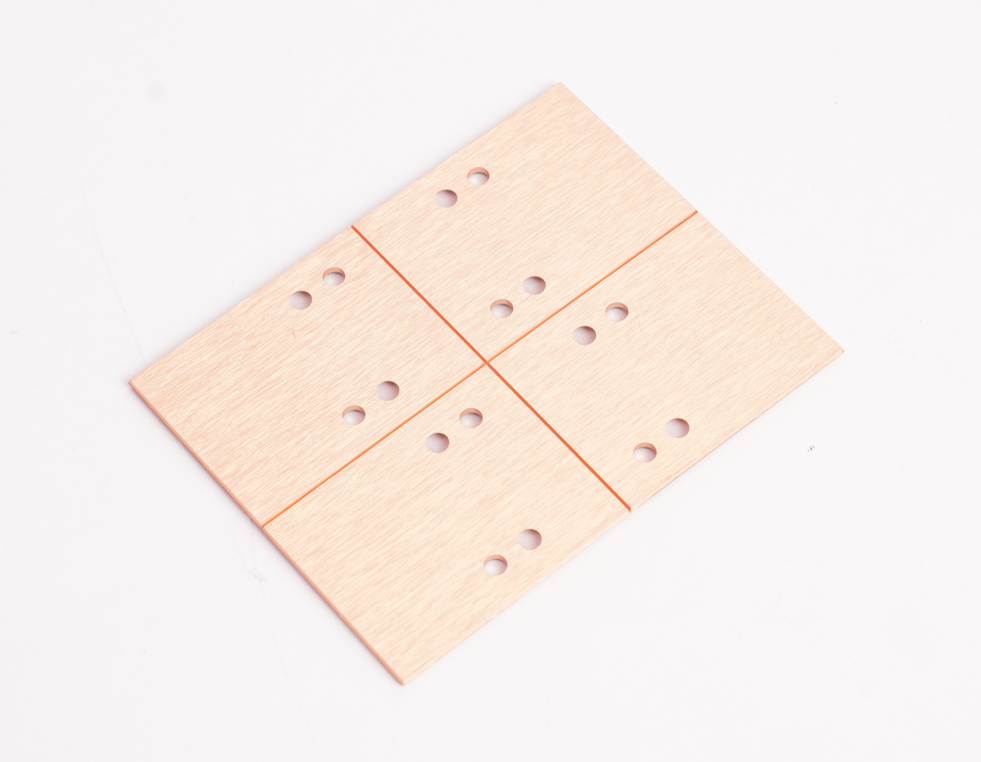
1. Substrate Preparation
- Select FR4 glass fiber epoxy resin laminate as substrate, with copper foil cladding (thickness 1oz/2oz).
2. Inner Layer Pattern Transfer:
- Apply photosensitive dry film, transfer circuit pattern via UV exposure, and dissolve unexposed areas.
- AOI (Automatic Optical Inspection) verifies line precision and marks defects.
3. Inner Layer Etching & Oxidation
- Chemically etch copper not protected by dry film to form inner layer circuits.
- Black oxide/brown oxide treatment on copper surfaces to enhance interlayer adhesion.
4. Lamination & Pre-Press
- Stack inner layer core boards, prepreg sheets, and outer layer copper foils alternately, aligning via positioning holes.
- High-temperature/high-pressure lamination (180-200℃) melts resin to fill gaps, forming a unified board.
5. Mechanical Drilling
- CNC drilling machine processes through-holes/blind holes with diameter accuracy ±0.05mm.
- Clean hole-wall resin residues (desmear).
6. Electroless Copper Plating
- Deposit electroless copper (0.3-0.8μm) on hole walls to establish conductive base.
- Electroplate to thicken copper layer (20-25μm) for reliable hole-wall conductivity.
7. Outer Layer Pattern Transfer
- Repeat inner layer pattern transfer process, addressing hole alignment.
- Use high-precision exposure equipment to compensate for interlayer deviation.
8. Outer Layer Etching & Stripping
- Secondary etching defines outer layer circuits, with tin layer protecting desired copper areas.
- Alkaline solution strips dry film, retaining circuit patterns.
9. Solder Mask & Silkscreen
- Apply liquid photosensitive solder mask (green/black), expose and develop to expose pads.
- Silkscreen component identifiers (white/yellow text).
10. Surface Finish
- Treat pad areas with ENIG (Electroless Nickel Immersion Gold)/immersion tin/OSP to prevent oxidation and enhance solderability.
- Plate gold finger areas with hard gold for wear resistance (e.g., board-edge connectors).
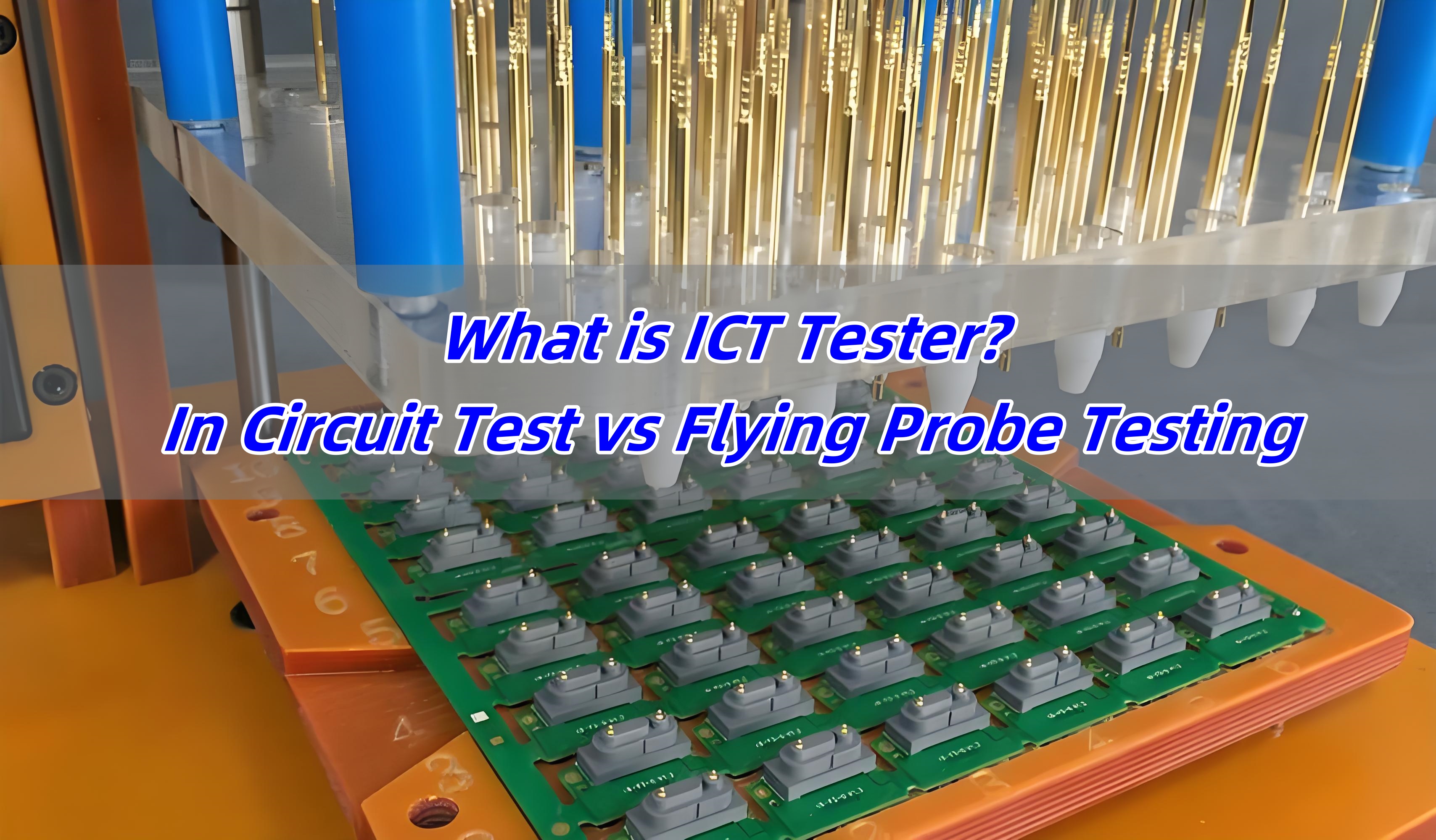
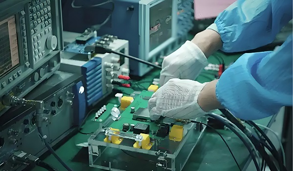
11. Electrical Testing
- Flying probe test or bed-of-nails test verifies continuity and insulation.
- AOI re-inspects for micro-shorts/opens.
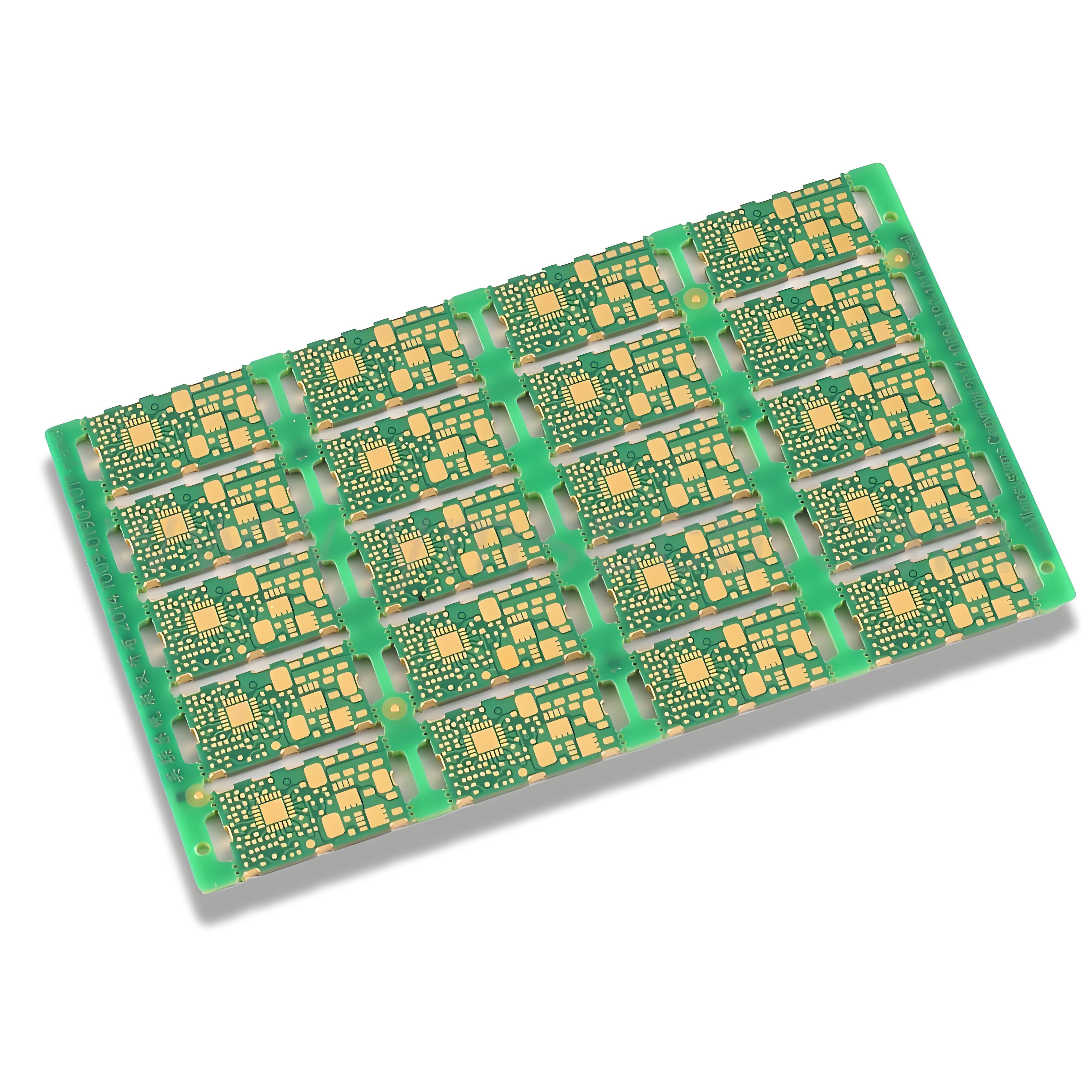
12. Profiling & Packaging
- CNC milling cuts board outlines; V-score or punching for separation.
- Final cleaning, drying, and vacuum moisture-proof packaging.
Why Choose EBest Circuit (Best Technology) as Copper Multilayer PCB Manufacturer?
Reasons why choose us as copper multilayer PCB manufacturer:
- 19 years of experience in copper substrate R&D: Precisely addressing interlayer heat dissipation and current carrying challenges in high-power multi-layer copper substrates, ensuring long-term stable operation of high-power devices (such as projectors/lasers).
- Triple international quality certification (ISO9001/IATF16949/ISO13485): Medical and automotive-grade copper substrate production standards ensure ±1μm copper thickness uniformity in multi-layer board holes and zero deviation in electrical performance.
- Customized thermal management solutions for copper substrates: Embedded copper pillars/thermoelectric separation structures reduce the thermal resistance of multi-layer boards to 0.5°C/W, extending the life of LEDs/power modules by over 30%.
- Cost-optimized copper substrate design: Utilizing a gradient copper foil thickness (1oz outer layer + 2oz inner layer) to balance conductivity and heat dissipation requirements, saving 15% in material costs compared to traditional designs.
- 24-hour copper substrate rapid prototyping service: Laser drilling and electroless copper plating processes deliver high-complexity (20+ layers) copper substrate prototypes within 48 hours, accelerating the validation cycle for high-power products.
- Free Copper Substrate Design for Material (DFM) Analysis: Preemptively identify design risks such as copper layer distribution and blind via alignment, preventing interlayer cracking caused by thermal expansion coefficient mismatch and reducing secondary re-board rework costs.
- 100% Automated Optical Inspection (AOI): Detects hole wall voids and copper nodules, a common feature of copper substrates, with a 0.01mm² level of defect detection, ensuring zero defective batch orders.
- Full-Process Copper Substrate Solution: From thermal simulation (Flotherm) to copper layer etching and surface treatment (ENIG/HASL), we provide a one-stop service, reducing the cost of coordinating multiple suppliers.
- Ultra-Thin Copper Substrate Process (0.2mm total thickness): Combining flexible PI substrate and copper foil calendering technology, we achieve a bend radius of less than 1mm for multi-layer copper substrates for wearable devices while maintaining a current density of 10A/cm².
Our Copper PCB Capabilities
| Items | Technical Parameters |
| Product model | Copper PCB |
| Copper trace thickness | 1OZ, 2OZ, 3OZ, 4OZ, up to 10OZ |
| Thermal Conductivity | 1.0, 1.5, 2.0, 3.0W/m.K |
| Surface finishing | HAL(LF)/ Gold Immersion/ Gold plating/ OSP/ Immersion Tin/ Silver Immersion |
| Soldermask Color | White/Black/Green/Blue/Red/Yellow |
| Layers | 1L, 2L, 4L, 6L, 8L, double sided, COB |
| Maximum dimension | 1,100mm*480mm; 1,500x300mm |
| Minimum dimension | 5mm*5mm |
| Minimum Line width/space | 0.1mm/0.1mm |
| Warp and twist rate | ≤0.75%(thickness:1.6mm, measurement:300mm×300mm) |
| Board Thickness | 0.3-4.5mm |
| Die-Punching dimension tolerance | ±0.15mm |
| V-cut positioning tolerance | ±0.1mm |
| Manufacturing capability | 6000m2 |
| Wall Cu thickness | 15-25um |
| Alignment tolerance | ±0.076mm |
| Minimum diameter of die-punching hole | Thickness <=1.0mm: 1.0mm |
| Thickness 1.2-3.0mm: 1.5mm | |
| Thickness 4.0mm: 2.0mm | |
| Minimum size the square groove/slot/cutout | Thickness <=1.0mm: 0.8mm×0.8mm |
| Thickness 1.2-3.0mm: 1.0×1.0mm | |
| Thickness 4.0mm: 1.5×1.5mm | |
| Outline Tolerance | CNC routing:±0.1mm; Die-punching:±0.15mm |
| Minimum diameter of hole | 0.3mm; not limit for maximum diameter of hole |
| Surface Finishing Thickness | gold plating:Ni 2.5-5um, Au: 0.025-0.075um |
| immersion gold: Ni 3-6um, Au: 0.025-0.1um | |
| HAL(LF): 3-30um | |
| V-cut Angle tolerance | ±5° |
| V-cut Range | 0.3mm-4.5mm |
| Smallest silkscreen height | 0.15mm |
| Smallest PAD | 0.1mm |
How to Get a Quote for Copper Multilayer PCB Project?
Essential Documentation for Copper Multilayer PCB Quotation
- Lamination Stackup Drawing: Specify layer materials (e.g., FR-4/Rogers 4350), copper thickness (1–6OZ), dielectric thickness (mm), and impedance control targets.
- Gerber Files: Include circuit layers, drilling layers, and solder mask layers. Annotate trace width/spacing (e.g., 4/4mil), blind/buried via positions, and hole tolerance (±0.05mm).
- PCB Technical Parameter Sheet: Board dimensions (L×W×T), layer count (e.g., 8L), surface finish (ENIG/OSP), and special processes (via plating/half-hole).
- Impedance Control Requirements: Define differential pair impedance (e.g., 100Ω±10%), reference layers, and testing methods.
- Acceptance Criteria: Specify IPC class (e.g., IPC-6012 Class 3) and testing items (flying probe/AOI/X-ray).
- Quantity & Lead Time: Prototype/batch quantity (e.g., 5pcs/1k) and desired delivery timeline (e.g., 7-day expedited).
- Special Requirements: High-frequency/thermal needs (e.g., PTFE hybrid), environmental certifications (RoHS/UL).
Why Partner with EBest Circuit (Best Technology)?
- Expertise: Handles 16+ layer thick copper (6OZ) and hybrid high-frequency boards.
- Speed: Offers 48-hour quick quotes and complimentary impedance calculation.
- Quality: Free DFM review to eliminate design flaws upfront.
- Result: Avoid cost overruns, accelerate time-to-market, and ensure compliance for demanding applications.
Welcome to contact us if you have any request for copper multilayer PCB: sales@bestpcbs.com.