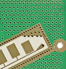
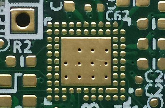
What is Via in Pad?
With the improvement of the integration of electronic products, the package of components is getting smaller and smaller, and the pin spacing is also getting smaller and smaller. In complex PCB design, the signal cannot be fanned out without punching the disc hole, and the signal must be drawn from the next layer through the disc hole. Especially in the miniaturization applications of BGA (Ball Grid Array) and SMD (Surface Mount Device) chips, the process of disc holes has been widely used.
Via in pad is a design methodology in PCB manufacturing where vias are directly embedded in the pads of surface-mount devices (SMDs). Traditional vias are placed near the components with traces connecting them to the pads. However, in via-in-pad designs, the vias and pads are combined, which saves space and shortens trace lengths. This approach is particularly useful in HDI PCBs, where board real estate is limited, and signal integrity is critical.
What is Via-in-Pad Plating?
Via-in-pad plating refers to a specialized manufacturing process where vias embedded in pads are filled and plated over to form a smooth, conductive surface. This process involves:
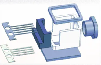
- Via Filling: The via hole is filled with a material, often epoxy or a conductive paste, to eliminate voids and provide structural stability.
- Copper Plating: The filled via is then plated with copper to create a uniform and conductive layer.
- Surface Finish: A finish such as ENIG (Electroless Nickel Immersion Gold) or HASL (Hot Air Solder Leveling) is applied to ensure solderability.
Proper via-in-pad plating prevents solder wicking, a phenomenon where solder flows into the via during reflow, causing insufficient solder on the component leads.
Is Via-in-Pad Expensive?
Via-in-pad designs are undeniably more expensive than traditional vias. The additional manufacturing steps, such as via filling, plating, and the need for precise alignment, contribute to the higher costs. Moreover, the advanced equipment and materials required for this process add to the overall expense.
However, for designs that demand high performance, such as smartphones, medical devices, and aerospace electronics, the benefits of via in pad often outweigh the cost. It allows for compact layouts, improved performance, and better thermal management, making it indispensable for cutting-edge applications.
What Size is a Via-in-Pad?
The size of a via-in-pad is influenced by the PCB’s application, layer count, and the size of the components used. In HDI PCBs, via sizes typically range from 0.15 mm to 0.4 mm in diameter. Microvias, often used in via-in-pad designs, can be as small as 0.1 mm.
The diameter must align with the pad size to avoid compromising the pad’s mechanical and electrical integrity. Designers also need to consider the PCB manufacturer’s capabilities when selecting via sizes, as extremely small vias may require advanced fabrication techniques.
What are the Drawbacks of Via in Pad?
While via in pad offers several advantages, it also comes with notable challenges:
- Higher cost
- Soldering defects
- Complex manufacturing
- Thermal stress risks
- Complex manufacturing process
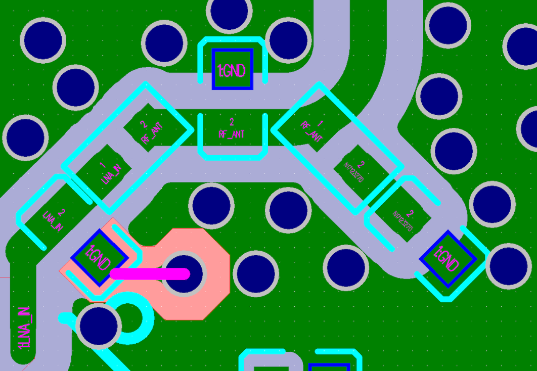
Can You Put Vias Under Components?
Yes, placing vias under components is common in advanced PCB designs, particularly with via in pad. This technique is often used for BGAs, QFNs, and other fine-pitch components.
However, proper design and manufacturing practices must be followed to prevent defects. Filling and plating the vias ensure they do not interfere with soldering. Additionally, simulations and testing are essential to validate the design and ensure reliability.
Traditional Vias vs. Via-in-Pad Design
Traditional vias are placed outside the component pad, with traces connecting them to the pads. While this approach is cost-effective, it consumes more space and may result in longer trace lengths, increasing parasitic effects.
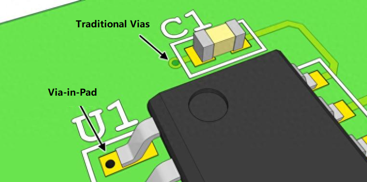
Via-in-pad designs embed the vias directly within the component pads, reducing trace lengths and optimizing space. They enhance signal integrity, thermal performance, and overall board aesthetics but at a higher cost and complexity.
When to Use Via-in-Pad Design?
Via-in-pad designs are not always necessary, but they are indispensable in specific scenarios where performance, space optimization, and thermal management are critical. Below are the situations where via-in-pad designs are most appropriate:
1. High-Density Interconnect (HDI) PCBs
When designing HDI PCBs with compact layouts and high layer counts, via-in-pad is essential. This design technique optimizes the limited space available, allowing for more components and connections on the board. It is particularly useful for devices like smartphones, wearables, and IoT devices where miniaturization is key.
2. Fine-Pitch Components
Via-in-pad designs are commonly used for components with fine pitches, such as:
- BGA chips: BGAs have numerous pins closely spaced, leaving minimal room for traditional routing. Via in pad provides a clean solution to connect signals directly.
- QFNs: QFNs require vias under the pads for effective routing and thermal management.
3. High-Speed and RF Applications
In high-speed and RF circuits, signal integrity is paramount. Via-in-pad designs minimize trace lengths, reducing parasitic inductance and impedance mismatches. This makes them ideal for applications like:
- 5G communication systems
- High-frequency radar systems
- Advanced networking equipment
4. Improved Thermal Management Needs
For power components or heat-sensitive devices, via in pad aids in efficient thermal dissipation. By directly connecting the pads to thermal vias leading to internal or external layers, heat is transferred away from the components. This is critical for:
- High-power LEDs
- Voltage regulators
- Power amplifiers
5. Limited PCB Real Estate
In designs with severe space constraints, via in pad maximizes usable board area. This allows for additional routing space and supports high component density without sacrificing performance. Applications like medical implants and aerospace electronics greatly benefit from this approach.
6. Double-Sided Component Placement
When components are placed on both sides of the PCB, traditional vias can interfere with the routing on the opposite side. Via in pad eliminates this issue by embedding the vias within the pads, simplifying double-sided designs.
7. High-Performance Computing Systems
For processors, GPUs, and other high-speed ICs, via in pad ensures reliable power delivery and signal integrity. It is frequently used in:
- Data centers
- High-performance workstations
- AI hardware
Guidelines for Via-in-Pad Design
Via-in-pad designs require meticulous attention to detail to ensure reliability and performance.
1. Decide on the most suitable via type based on your design requirements:
- Microvias: Ideal for high-density designs due to their small size.
- Blind/Buried Vias: Useful for connecting internal layers without penetrating through the entire board.
- Through-Hole Vias: Less common in via-in-pad but may be necessary for specific designs.
2. Fill the vias with appropriate materials to ensure mechanical stability and prevent solder wicking:
- Non-Conductive Epoxy Fill: Provides a reliable, flat surface for soldering.
- Conductive Fill: Used when electrical connectivity through the via is needed.
3. The plating over the filled vias should be smooth and flat to avoid soldering issues. Use a high-quality copper plating process to enhance electrical and thermal conductivity.
4. Collaborate with your PCB manufacturer early in the design process to align on their capabilities. This includes:
- Minimum via diameter and pad size.
- Spacing requirements between vias and traces.
- Maximum number of vias that can be placed in pads.
5. Ensure the via size is proportionate to the pad size. A via that is too large can compromise the pad’s structural and electrical integrity, while a too-small via may not provide the necessary connectivity or thermal performance.
6. For high-power applications, incorporate thermal relief patterns or thermal vias.
7. Maintain sufficient spacing between vias and other components or traces to prevent electrical interference or thermal stress.
8. To avoid solder flowing into the via during reflow soldering:
- Use filled and capped vias.
- Employ surface finishes like ENIG (Electroless Nickel Immersion Gold) or OSP (Organic Solderability Preservative) for enhanced soldering reliability.
9. When using via in pad for power components or ground connections, thermal relief patterns help prevent excessive heat buildup. These are especially important in high-current designs.
Need assistance in designing via-in-pads in your PCB design? Leave your comments on below, our design experts will help to solve them.