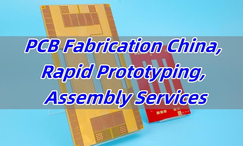
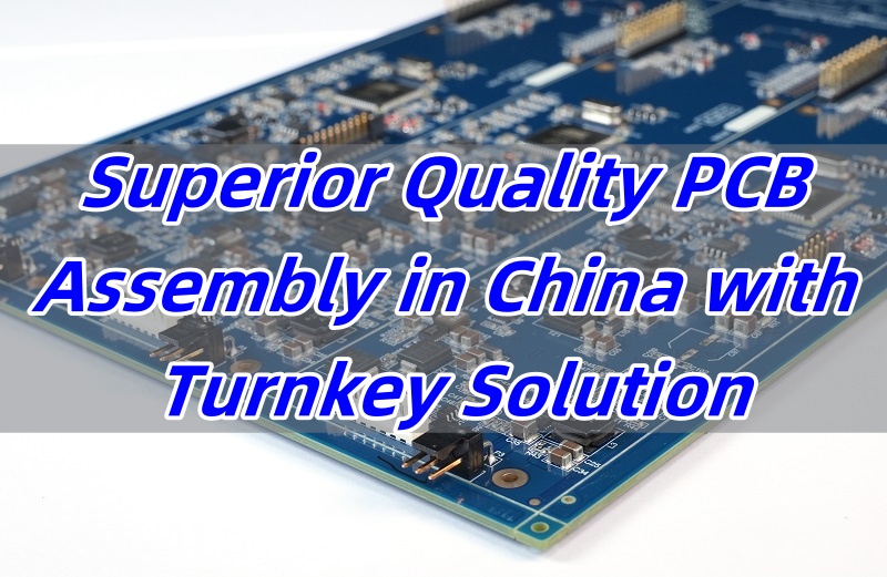
PCB assembly in China has gained global recognition for its fast delivery and growing quality standards. But not all services are the same. Let’s dive into what defines a premium service, who the top players are, and why EBest Circuit (Best Technology) stands out.
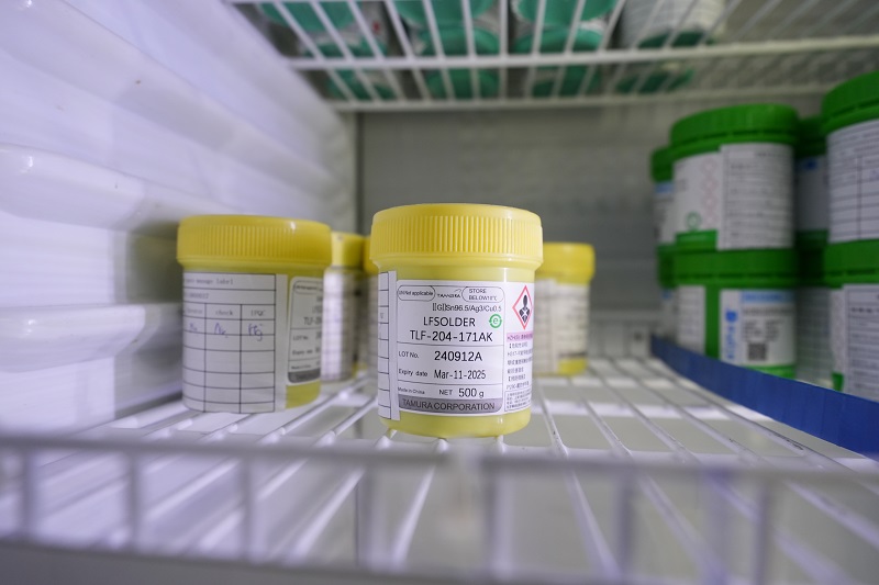
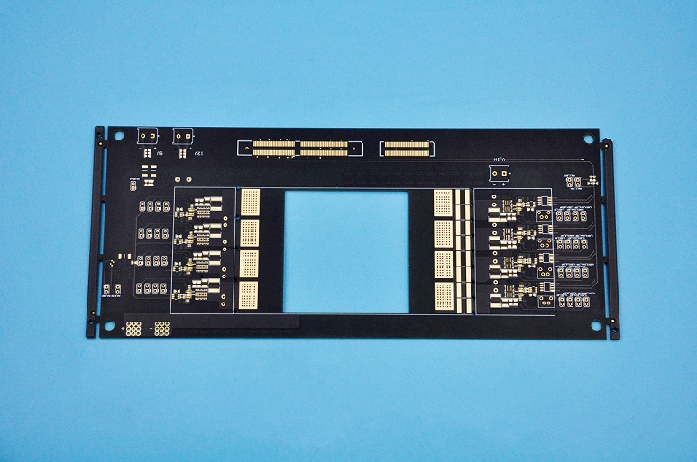
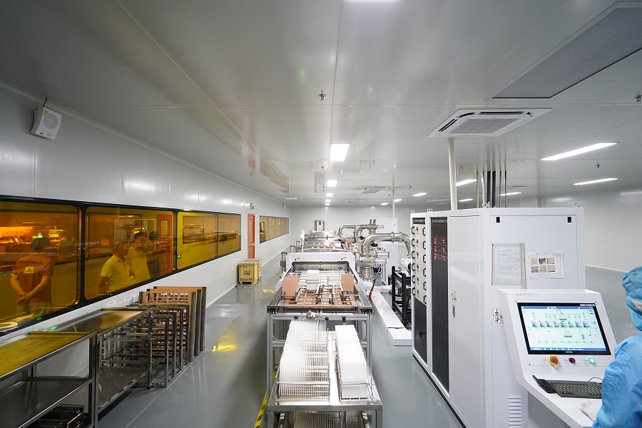
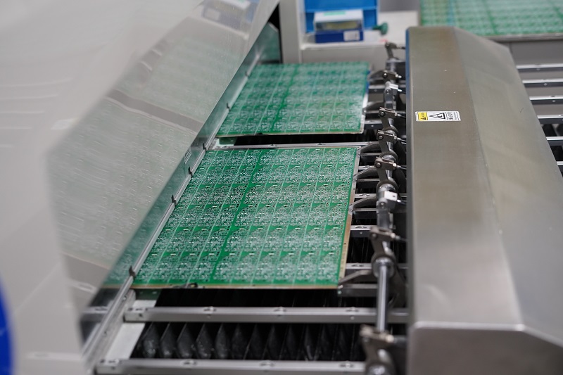
EBest Circuit (Best Technology) has SMT factories in China and Vietnam respectively providing superior quality PCB assembly in China with turnkey solutions. Our SMT workshops are ISO 9001, ISO 13485, IATF 16949, and AS9100D compliant. In a competitive world market, we are realizing that it’s more important than ever to hold onto our competitive edge, such as premium quality, supply chain integrity, on-time guarantee, and agile response. Our PCBA is widely used in industrial-grade high-end services and the medical, and aerospace industries. Kindly email us at sales@bestpcbs.com if you have any inquiries.
What Defines a Premium PCB Assembly Service in China?
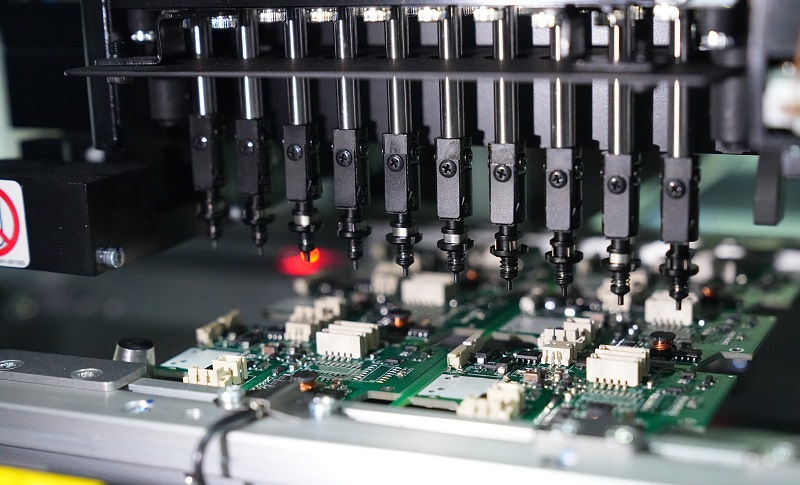
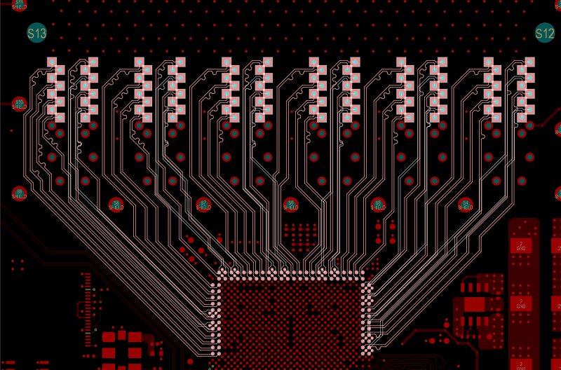
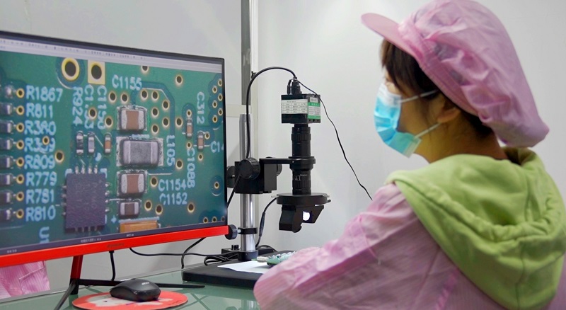
High-quality PCB assembly is more than just good soldering. A premium service delivers accuracy, traceability, and fast turnaround without compromising on reliability. In China, top providers focus on:
- Full traceability – so you know the source of every component
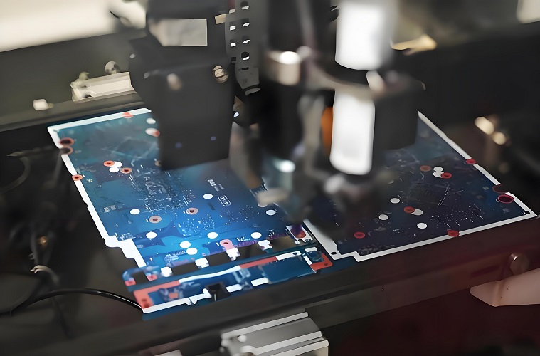
- Advanced testing – including AOI, ICT, X-ray, and functional tests
- Strict process control – to reduce defects like misalignment or cold joints
- Real-time updates – to keep clients informed on order progress
Providers lacking these usually face recurring quality issues, such as component misplacement, contamination, or invisible soldering faults.
Who Are the Best Manufacturers of PCB Assembly in China?
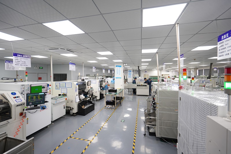
The top PCB manufacturers in China lead with consistent quality, strong supply chains, and smart engineering support. Many of them are based in Shenzhen, where access to raw materials and labor is easier. Some reliable names include:
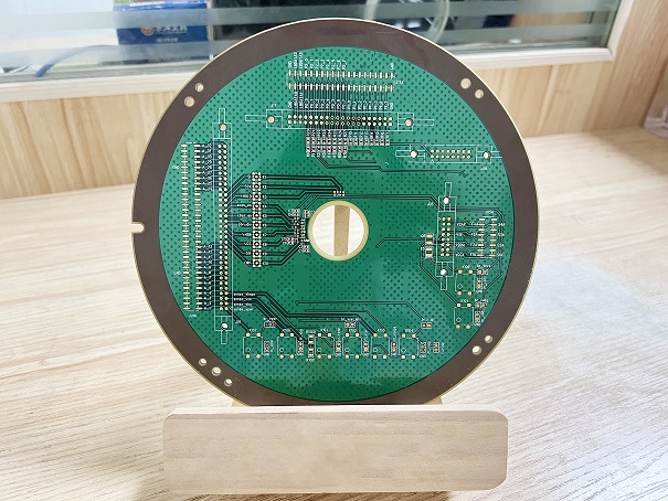
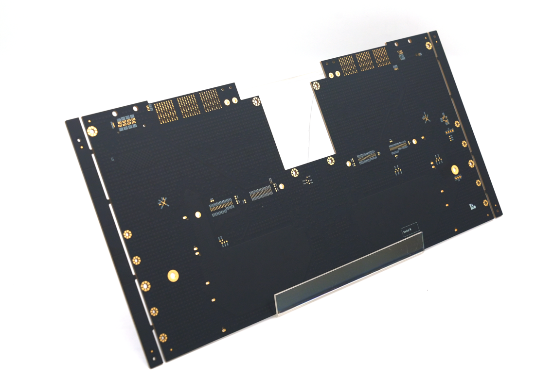
- EBest Circuit (Best Technology): EBest Circuit (Best Technology) is a professional PCB assembly manufacturer in China known for its one-stop solution covering design support, prototyping, and mass production. With quality traceability, strong engineering support, and reliable supply chain management, EBest Circuit (Best Technology) helps clients overcome challenges in delivery timelines, communication, and quality consistency.
| Item | Capabilities |
|---|---|
| Placer Speed | 13,200,000 chips/day |
| Bare Board Size | 0.2 x 0.2 inches – 20 x 20 inches/ 22*47.5 inches |
| Minimum SMD Component | 01005 |
| Minimum BGA Pitch | 0.25mm |
| Maximum Components | 50*150mm |
| Assembly Type | SMT, THT, Mixed assembly |
| Component Package | Reels, Cut Tape, Tube, Tray, Loose Parts |
| Lead Time | 1 – 5 days |
- Hitech Circuits: Hitech Circuits Co., Ltd. is a Shenzhen-based PCB and PCBA manufacturer with a global presence. They specialize in multilayer PCBs, HDI boards, and quick-turn prototypes.
- Shenzhen Sunthone: Shenzhen Sunthone Electronics Co., Ltd. offers full-service PCB fabrication and assembly. They focus on low to medium volume production with fast delivery. Their core strengths include strong SMT capabilities and multiple quality testing procedures. Sunthone supports clients from various industries such as IoT, LED, and smart appliances, and is well-known for its customer-first service philosophy and fast communication.
These companies combine quick delivery with high-volume capabilities and tight quality control.
Is Best Based in China?
Yes. EBest Circuit (Best Technology) is located in Shenzhen. This gives access to advanced PCB manufacturing machines and stable sourcing channels. We follow international standards such as ISO 9001, IATF 16949, ISO 13485, and AS9100D, serving automotive, medical, and aerospace sectors.
Where Are Most PCB Assembly Manufacturers in China?
Most PCB assembly manufacturer in China are clustered in Shenzhen, Dongguan, Suzhou, and Zhongshan. These hubs offer lower logistics costs, flexible labor, and better access to key materials. That’s why sourcing PCB assembly in China from these areas can offer speed and value.
How Expensive is it to Make a Custom PCB Assembly in China?
Costs vary by volume, layer count, and components. But even with customization, prices in China stay competitive. Thanks to automation and smart sourcing, PCB assembly in China can cost 30–50% less than in the USA or Europe. For example, EBest Circuit (Best Technology) uses ERP and MES systems to reduce labor waste and improve yield.
How to Get a Reliable PCB Assembly Service in China?
Start by checking certifications, experience, and communication ability. Ask about:
- Whether they support design for manufacturability (DFM)
- How they track materials and components
- What quality checks are used
At EBest Circuit (Best Technology), we not only provide quick responses and detailed BOM reviews, but we also support international customers through bilingual engineers. That’s how we remove cultural and technical gaps.
Why Choose EBest Circuit (Best Technology) for Reliable PCB Assembly in China?
EBest Circuit (Best Technology) offers a one-stop PCB solution, solving the key issues most customers face:
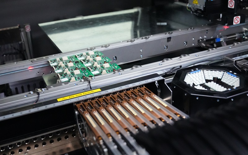
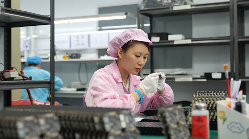
1. Strong Quality Management
We use MES systems for traceability. Each PCB has its own data, so tracking errors becomes easy. Our AOI, X-ray, and in-circuit tests catch 98% of potential faults before delivery.
2. Stable Supply Chain
We manage multiple supplier sources to avoid delays. With mature supplier networks, we quickly adapt to shortages or price changes. This ensures you get stable delivery timelines even in uncertain markets.
3. Fast Prototyping & Scale-Up
We offer rapid prototyping, small batch runs, and large-scale production. From design support to material sourcing, we reduce lead time and allow for smooth market entry.
In essence, whether you need a quick-turn prototype or full-scale production, PCB assembly in China is a smart option. But only if the partner can meet the challenges—traceability, supply chain risks, and technical updates. EBest Circuit (Best Technology) helps you succeed with its complete turnkey solution. We give you more than a PCB. We give you practical solutions—in DFM analysis, in delivery, in quality, and in results. Ready to start your next project? Feel free to send us an e-mail at sales@bestpcbs.com to get a quote now.