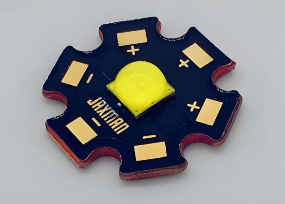
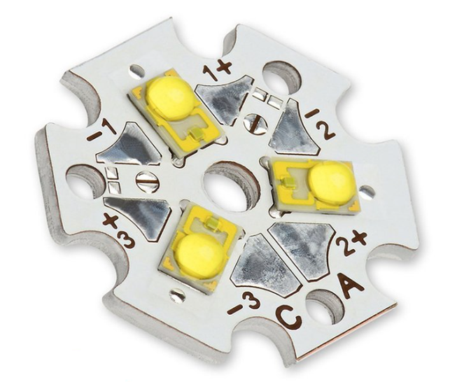
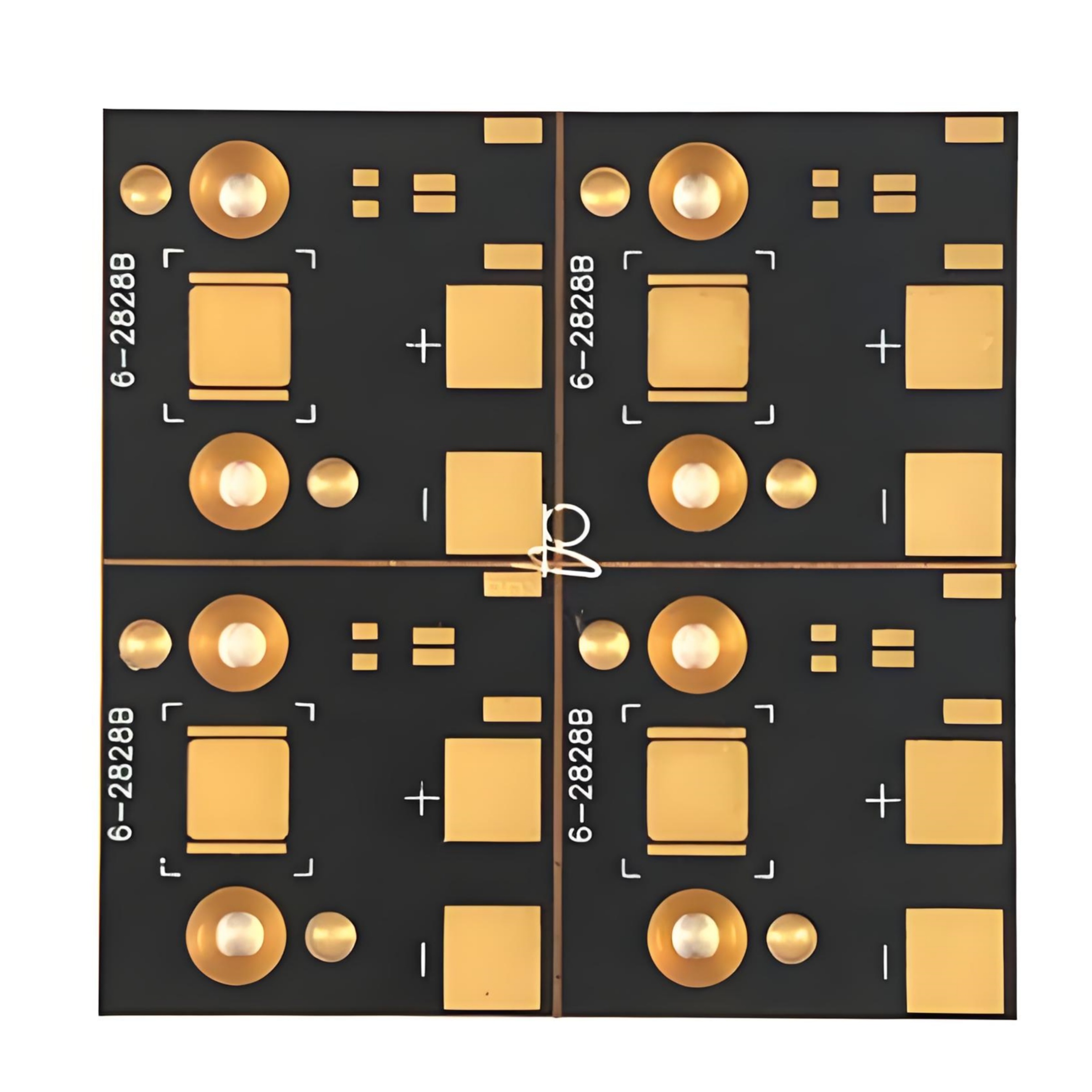
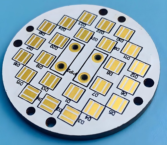
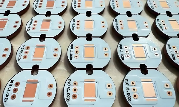
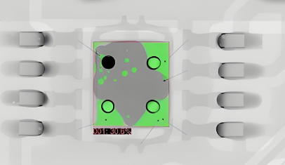
If you’ve ever worked with Metal Core PCBs (MCPCBs), or copper-clad boards, you’ve likely appreciated their superb ability to whisk heat away from powerful components like LEDs or power converters. But this very strength introduces a unique and frustrating weakness: the dreaded pad lift.
There’s little more disheartening than seeing a copper pad, along with your carefully soldered component, physically peel away from the board during assembly or rework. This isn’t a simple soldering mistake; it’s a fundamental battle between physics and materials that you lost. But it’s a battle you can win.
This blog post will dive deep into the why and, more importantly, the how—how to prevent this costly issue from plaguing your projects.
What Cause Pads Lift on Copper-Clad Boards?
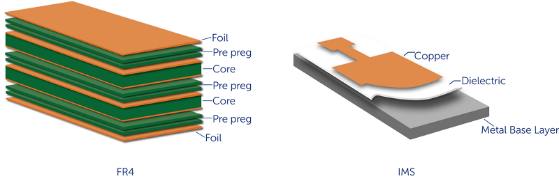
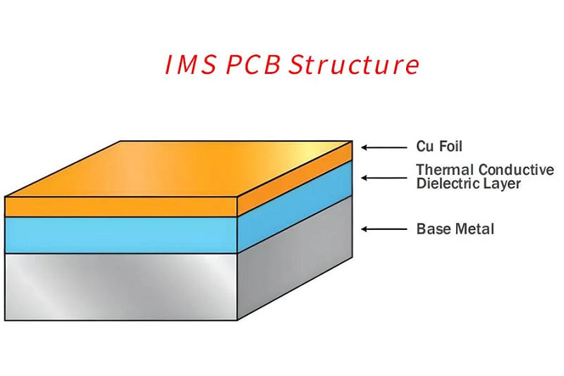
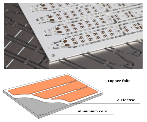
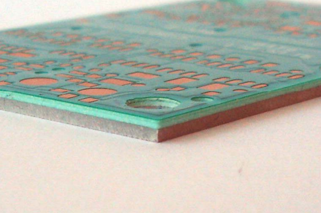
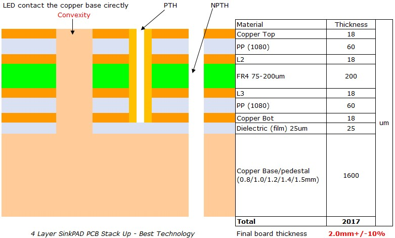
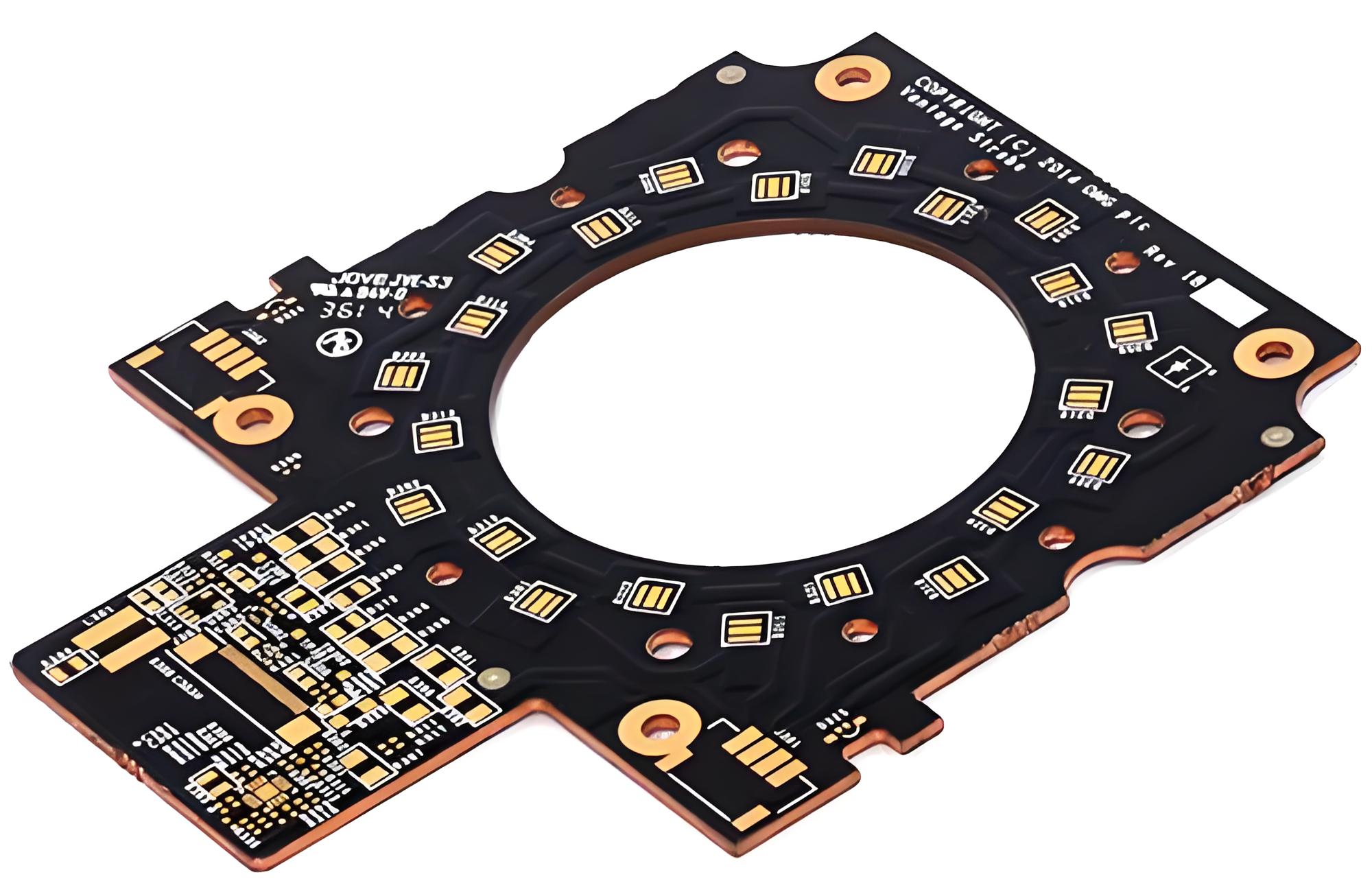
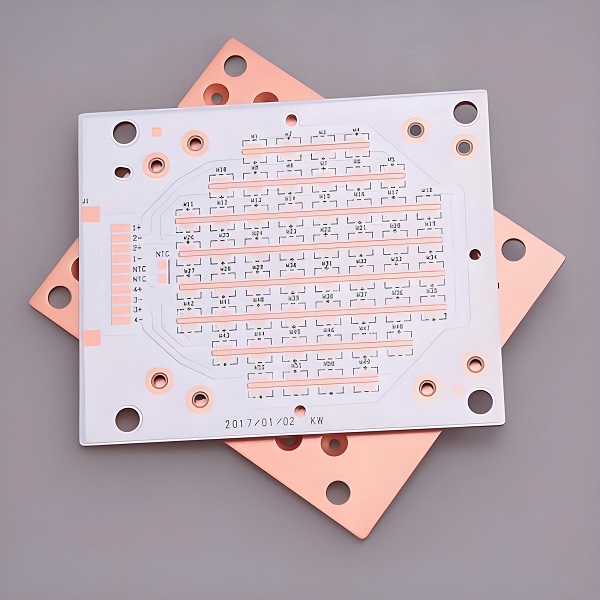
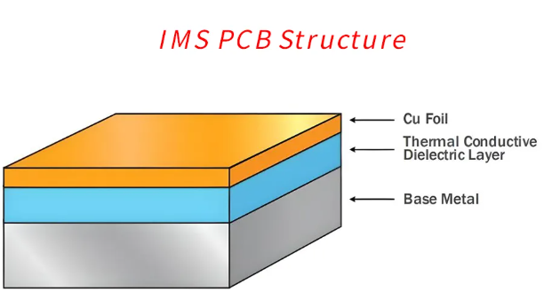
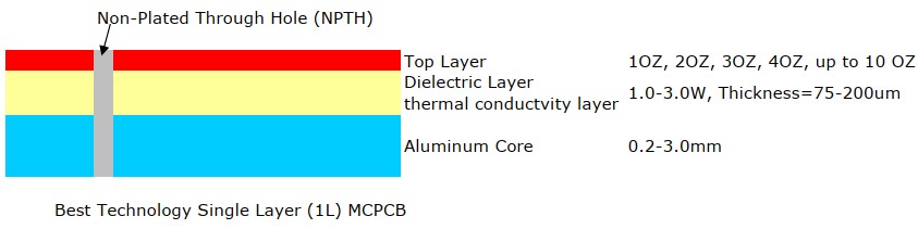
To understand why pad lifting happens, we must first look at the structure of a typical Copper MCPCB:
1. Copper Circuit Layer: The thin layer where your traces and pads are etched.
2. Dielectric Insulating Layer: A critical polymer-based layer (often epoxy with ceramic fillers) that electrically isolates the circuit from the metal base. It’s also the primary thermal conduit.
3. Copper or Aluminum Base Plate: The thick metal core that acts as a massive heat sink.
The problem lies in their Coefficients of Thermal Expansion (CTE). Copper and aluminum have very similar CTEs. The dielectric layer, however, has a CTE that is vastly different. When you subject the board to the high temperatures of a soldering process (200-260°C+), these layers expand at dramatically different rates.
Upon cooling, they contract at different rates again. This mismatch creates immense shear stress right at the interface between the copper pad and the dielectric layer. When this internal stress exceeds the adhesive strength (the “peel strength”) bonding the copper to the dielectric, the pad delaminates and lifts off.
This fundamental CTE mismatch is a given. The goal, then, is to manage the forces and strengthen the system to prevent failure.
What Actually Pushes a Pad to Lift?
Several factors in design, manufacturing, and assembly act as the “last straw” that triggers a pad lift.
1. Thermal Shock During Assembly & Rework
This is, by far, the number one cause.
- Excessive or Prolonged Rework: Every time you apply a soldering iron to a pad, you create a localized, extreme thermal cycle. The pad heats up and expands rapidly, while the surrounding area remains cooler. Multiple rework attempts fatigue the bond, progressively weakening it until it fails. The higher the iron temperature and the longer the contact time, the greater the risk.
- Incorrect Soldering Iron Use: Using an overpowered iron, a tip that’s too small (forcing you to hold it longer), or applying excessive pressure to “squeeze” heat out, all contribute to thermal shock and mechanical damage.
- Aggressive Reflow Profiles: An oven profile with too high a peak temperature or excessive time above liquidus can “cook” the dielectric layer, weakening its adhesive properties across the entire board.
2. PCB Design Flaws
The board’s layout can set the stage for failure from the very beginning.
- Poor Thermal Relief Design: A pad directly connected to a large copper pour for thermal management acts as a massive heat sink. To melt the solder, you must pump in far more heat for a longer duration, dramatically increasing the thermal stress on the pad’s connection point. This is the most common design-related mistake.
- Isolated Pads: Conversely, a pad with no thermal connection can heat up too quickly, creating a severe thermal gradient and concentrating stress upon cooling.
3. PCB Manufacturing Quality
Not all MCPCBs are created equal.
- Low Peel Strength: The core specification for pad adhesion is the Copper Foil Peel Strength. Low-quality laminates simply have inferior bonding between the copper and the dielectric layer, offering less resistance to the inherent thermal stress.
- Drilling and Fabrication Issues: Poor drilling quality can cause micro-fractures or delamination around via holes, creating a weak point from which a pad can start to lift.
4. Mechanical Stress
Physical forces can work in tandem with thermal stress to finish the job.
- Installation Stress: Over-tightening the screws when mounting the MCPCB to a heatsink can warp the board. This pre-stresses the copper-dielectric bond, making it much more susceptible to failure during the subsequent soldering heat cycle.
- Component Stress: Heavy components or components with stiff leads can exert constant mechanical leverage on the pads, especially under vibration.
How to Prevent Pad Lifting?
Fixing pad lifting requires a systematic approach across design, sourcing, and assembly.
1. Master the Soldering Process (The Most Critical Step)
- Control Time and Temperature: Use a temperature-controlled iron. Set it to the lowest effective temperature (typically 350-380°C for lead-free solder) and adhere to the “3-to-5 Second” rule: complete the joint within 3 seconds, and never exceed 5 seconds of continuous contact.
- Limit Rework: Establish a strict limit—if a joint isn’t right after 2-3 attempts, stop. Let the board cool completely and re-evaluate your approach. Forcing it will only lead to failure.
- Use the Right Tool: Match your soldering tip size to the pad and component. A larger, chisel tip transfers heat more efficiently than a fine point, reducing the time needed.
2. Implement Smart PCB Design
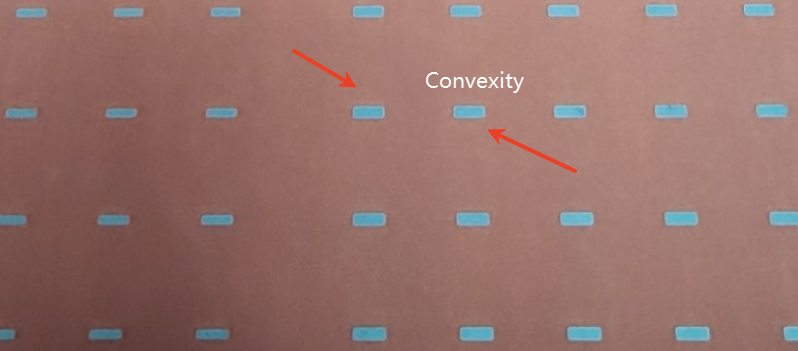
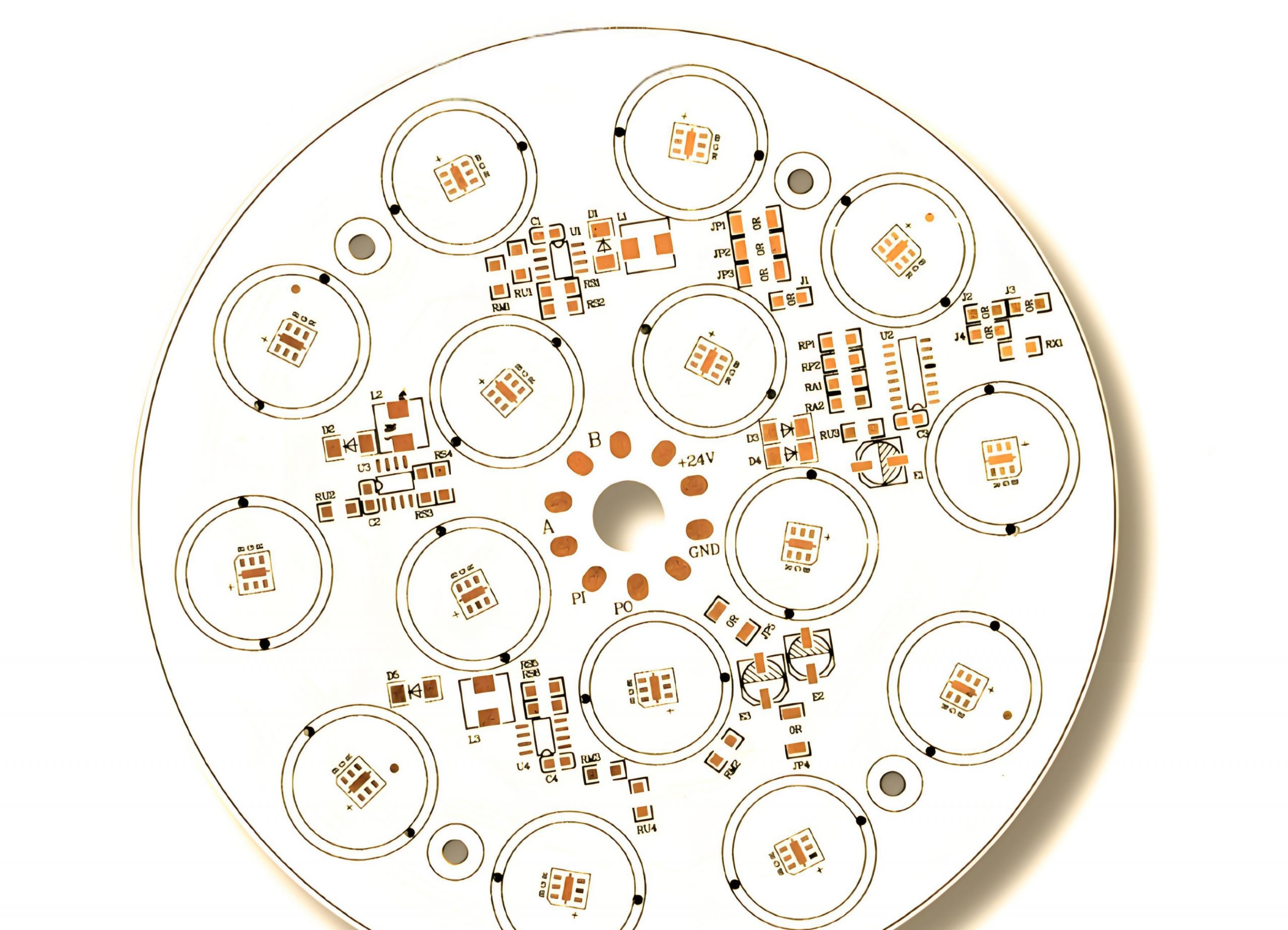
- Use Thermal Relief Pads (The Golden Rule): This is the single most effective design change. Instead of connecting a pad directly to a copper plane, use a “spoked” or “cross-hatched” connection. These thin traces provide sufficient electrical and thermal conductivity while significantly increasing the thermal resistance during soldering. This allows the pad to heat up quickly without stealing all the heat away, minimizing the thermal stress.
- Reinforce Pads: Use teardrops at the junction of pads and traces to add mechanical strength. Where possible, slightly increase the pad size to improve adhesion.
3. Source High-Quality Materials
- Specify High Peel Strength: When ordering your MCPCBs, don’t just shop for price. Consult with your manufacturer and specify a material with a high copper peel strength. Reputable laminate suppliers (like Bergquist or Laird) provide these specifications.
- Audit Your PCB Supplier: Work with a fabricator who has proven experience with MCPCBs and understands the rigorous demands of the assembly process.
4. Refine Mechanical Assembly
- Control Torque: Use a torque screwdriver when mounting the board to a heatsink. Follow the manufacturer’s recommended torque values and tightening sequence to avoid warping.
- Support Heavy Components: For large parts, use adhesive or additional mechanical fasteners to secure the component body, relieving the strain on the solder joints and pads.
Conclusion
Pad lifting on MCPCBs isn’t random. It’s the result of predictable stress acting on a thin copper-dielectric interface. When that stress rises above the material’s peel strength, the pad lets go.
But you can prevent it.
- Solder smarter with tight control of heat and dwell time.
- Use thermal relief features in your design.
- Choose MCPCB materials with high peel strength.
- Avoid mechanical stress during assembly.
Once you align your design, materials, and soldering process with the thermal realities of MCPCBs, your pad-lifting issues drop dramatically—and your yield, reliability, and confidence rise just as quickly.