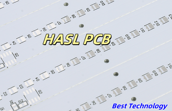
PCB printed circuit boards are essential to achieving the functionality of electrical devices, but before the final board can be manufactured, a carefully drawn schematic is essential. The PCB schematic is the blueprint that guides the actual design and manufacture of the circuit board. The schematic and Gerber files are key elements in the PCB manufacturing process, and each plays a different role.
What is the schematic file for PCB?
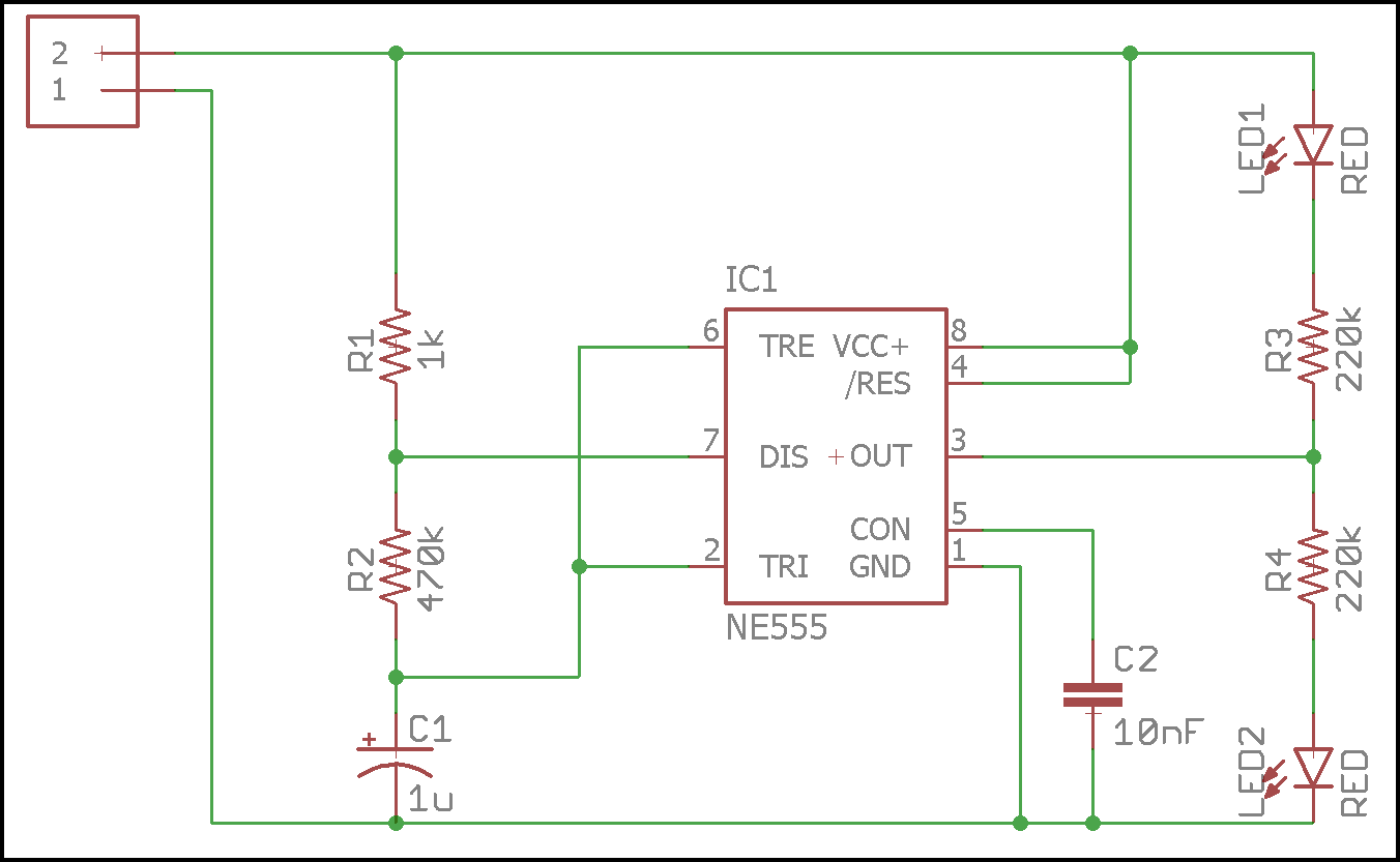
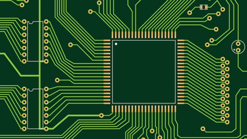
The schematic file is the foundation of any PCB design. It represents the logical connections and relationships between different components in the circuit. Think of it as a map showing how each component, such as resistors, capacitors, and microcontrollers, is connected to form a functional circuit.
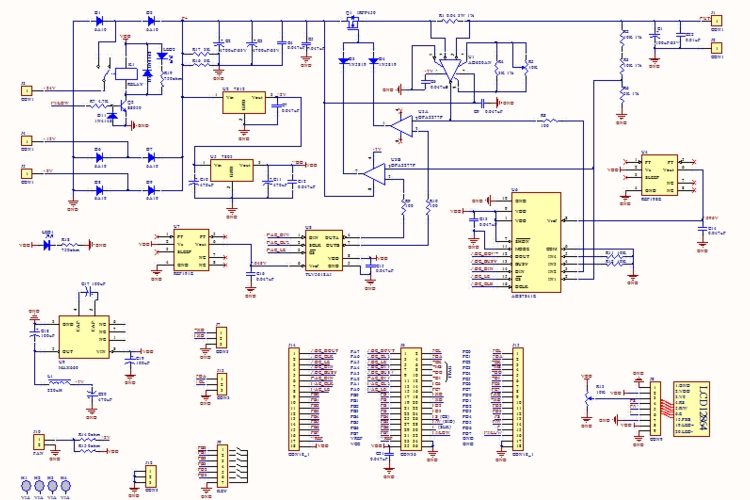
When creating a PCB, the schematic file is the first step. It is used to document the design and is essential to ensure that the final product functions as expected. Engineers use specialized software to create these schematic files, which can then be converted into the layout of the physical PCB.
What is PCB CAD file?
PCB CAD files are files directly output or saved by EDA software for PCB design. These files contain information about each layer of the PCB, network connection information, component information, etc. They are very comprehensive and contain almost all the information of the circuit board.
This format is mainly used for the storage and exchange of circuit board design, and contains information such as the layout, connection, pad, and drilling of each component on the circuit board.
In circuit board design, designers use circuit board design software to draw circuit schematics, layout, connection, component placement, etc., and finally generate a PCB file, and then load the file onto the circuit board to realize the production of the circuit board.
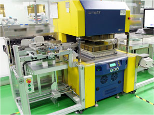
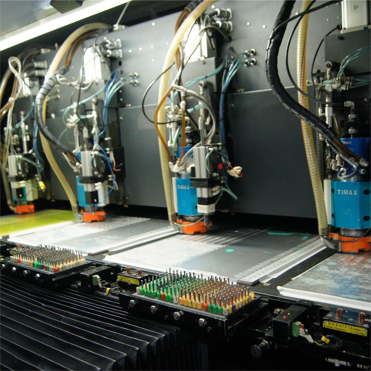
In addition, PCB CAD files play an important role in the offline programming of SMT placement machines. Offline programming refers to the work of compiling SMT placement programs on a computer using offline programming software and PCB CAD design files.
This programming method can save online programming time, thereby reducing the downtime of the entire PCBA processing and improving the utilization of equipment. Offline programming software is often used in automated production processes to ensure efficient and accurate completion of the placement of electronic components.
What files are needed to make a PCB?
Creating a PCB is a multi-step process involving multiple different files, each with its own unique purpose.
1. Schematic file (.sch, .dsn): represents the logical connection of the circuit and is the blueprint of the entire PCB design process.
2. Netlist file (.net, .xml): generated based on the schematic, lists all components and their connections.
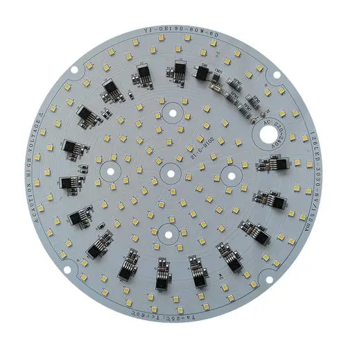
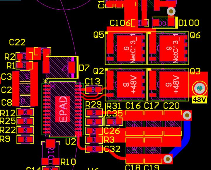
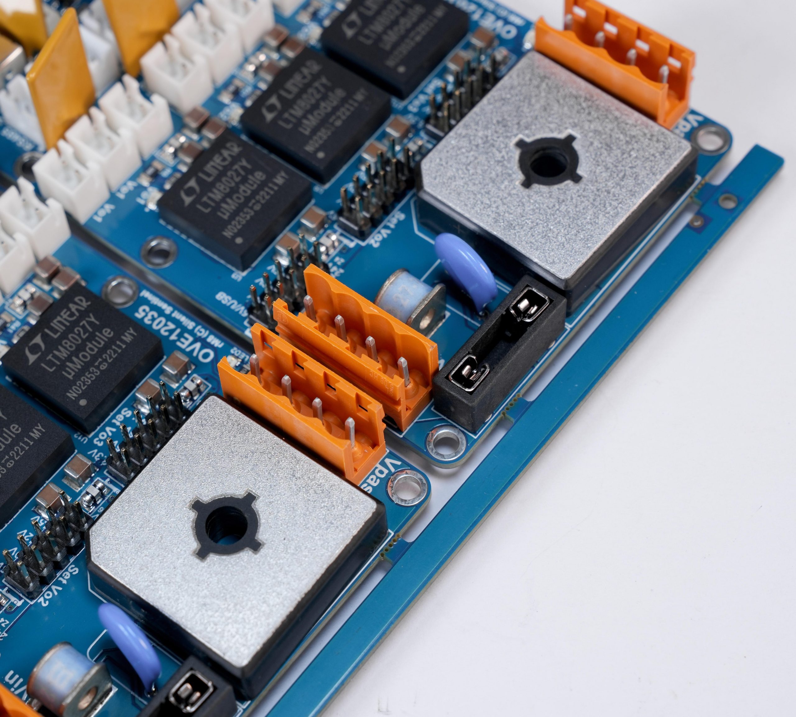
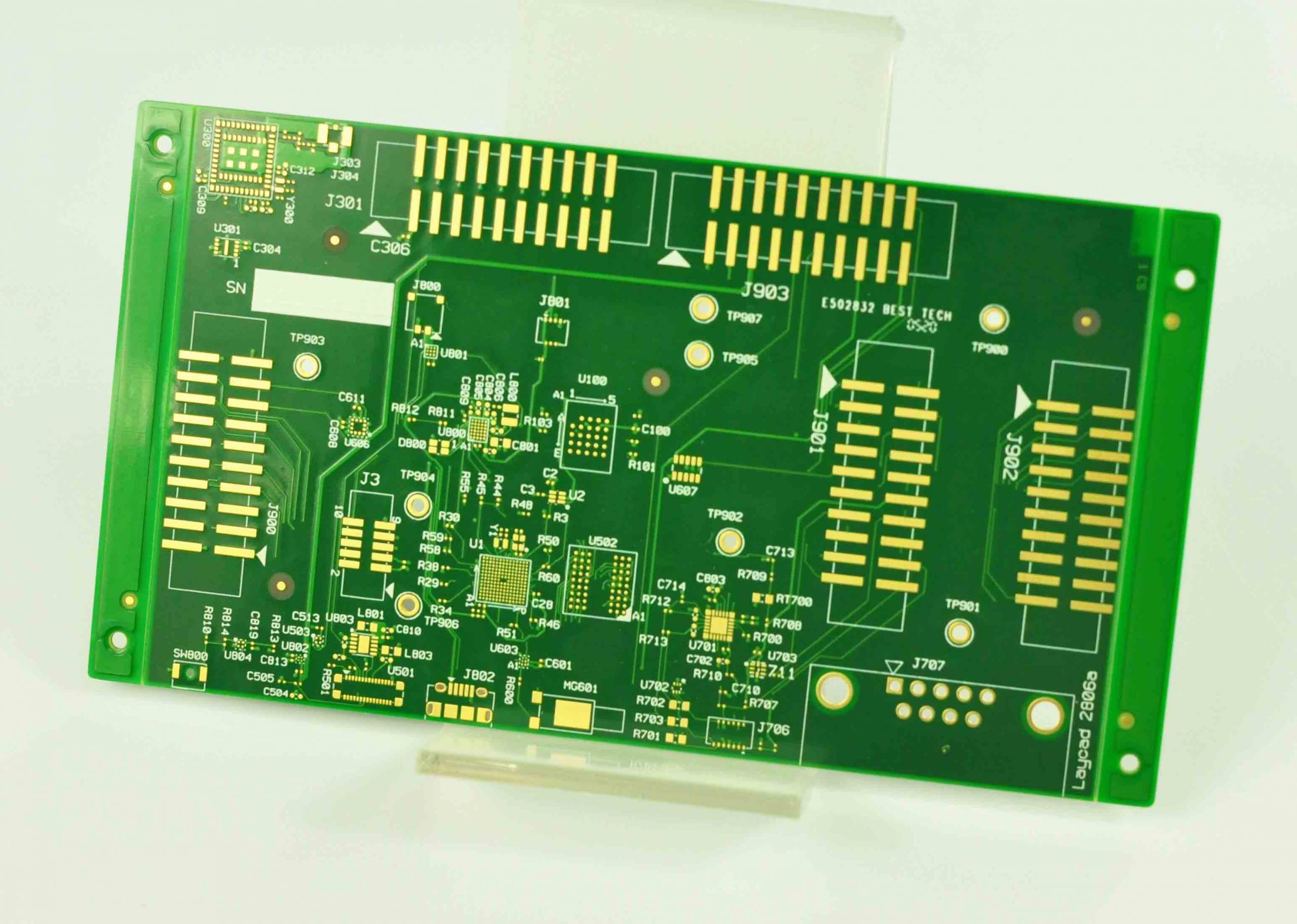
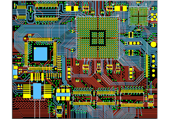
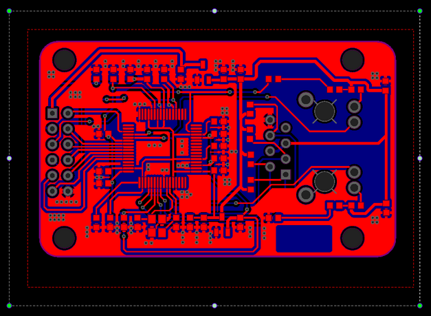
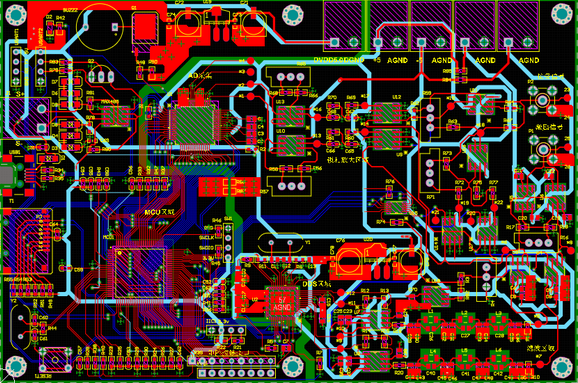
3. Gerber file (.gbr, .pho): Gerber file is the most important file for manufacturing PCB. Define each layer of the PCB, including copper wire, solder mask and silk screen printing layer, each layer of the PCB requires its own Gerber file.
4. Drill file (.drill, .drl): specifies the location of the holes drilled on the PCB. It includes information on the size and location of each hole.
5. Bill of Materials (BOM, .bom, .csv): BOM lists all the components required to assemble the PCB. Including part number, quantity and other details required for procurement.
6. Pick and place file (.txt, .csv): used in the assembly process to specify the precise location of each component on the circuit board.
What is the file type for circuit schematic?
The file type for a circuit schematic can vary depending on the software used to create it.
1. .SCH: This is the most common file extension for schematic files.
2. .DSN: This is another standard for schematic files.
3. .PDF: Although PDF is not a design file, it is often used to share schematics for review. It provides a non-editable version of the schematic that can be easily viewed.
4. .XML: Some tools export schematics as XML files for compatibility with other software. This format is useful for exchanging data between different design tools.
5. .PNG/.JPG: Image formats such as PNG or JPG are sometimes used to share simple schematics. These are not editable, but can provide a quick way to visualize the circuit.
What does a Gerber file contain?
Gerber is actually a description file that focuses more on PCB manufacturing and production. It should be said that it was originally designed for plotters. Therefore, the content of Gerber basically includes the information required for PCB manufacturing, such as copper foil circuit layer, solder mask layer, silk screen layer, legend layer, drill layer, etc. Even solder paste printing layer, image recognition layer, annotations and production notes can be included in it in layers.
Advantages and Disadvantages of Gerber Files
Gerber files are not suitable for being used as a storage file format for current PCB design. Because the Gerber file format does not contain the connection information between the various circuit layers of the PCB.
If you look closely at the Gerber file structure, you will find that each layer is a small file, which means that the layers of Gerber are independent and unrelated to each other. They are like independent drawings. This feature had little impact on wiring engineers when PCBs were only single-sided or double-sided in the early days, but it is very disadvantageous in design, operation, debugging and verification for the increasingly complex multi-layer PCBs. Therefore, almost no one uses Gerber files as the file format for PCB design.
Because the amount of information in Gerber files is small, its file size is much smaller than other design files drawn by EDA or CAD software. In addition, its format is more irreversible in design and protects the original design. In addition, its vector image layered format is still very suitable for use in PCB manufacturing. Today, PCB production generally follows this layer to divide the process into different stages for production, so Gerber files are still widely used in PCB production.
Therefore, some design companies with high confidentiality requirements will convert the design files into Gerber before sending them to the PCB factory for production, trying to keep confidentiality.
Conclusion:
For anyone working in the electronics industry, it is essential to understand the various file types used in PCB design. From the initial schematic file to the final Gerber file, every step in the design process relies on accurate and compatible files. BEST Technology has a professional PCB design team with rich experience in different PCB designs. We can solve all your PCB design problems.