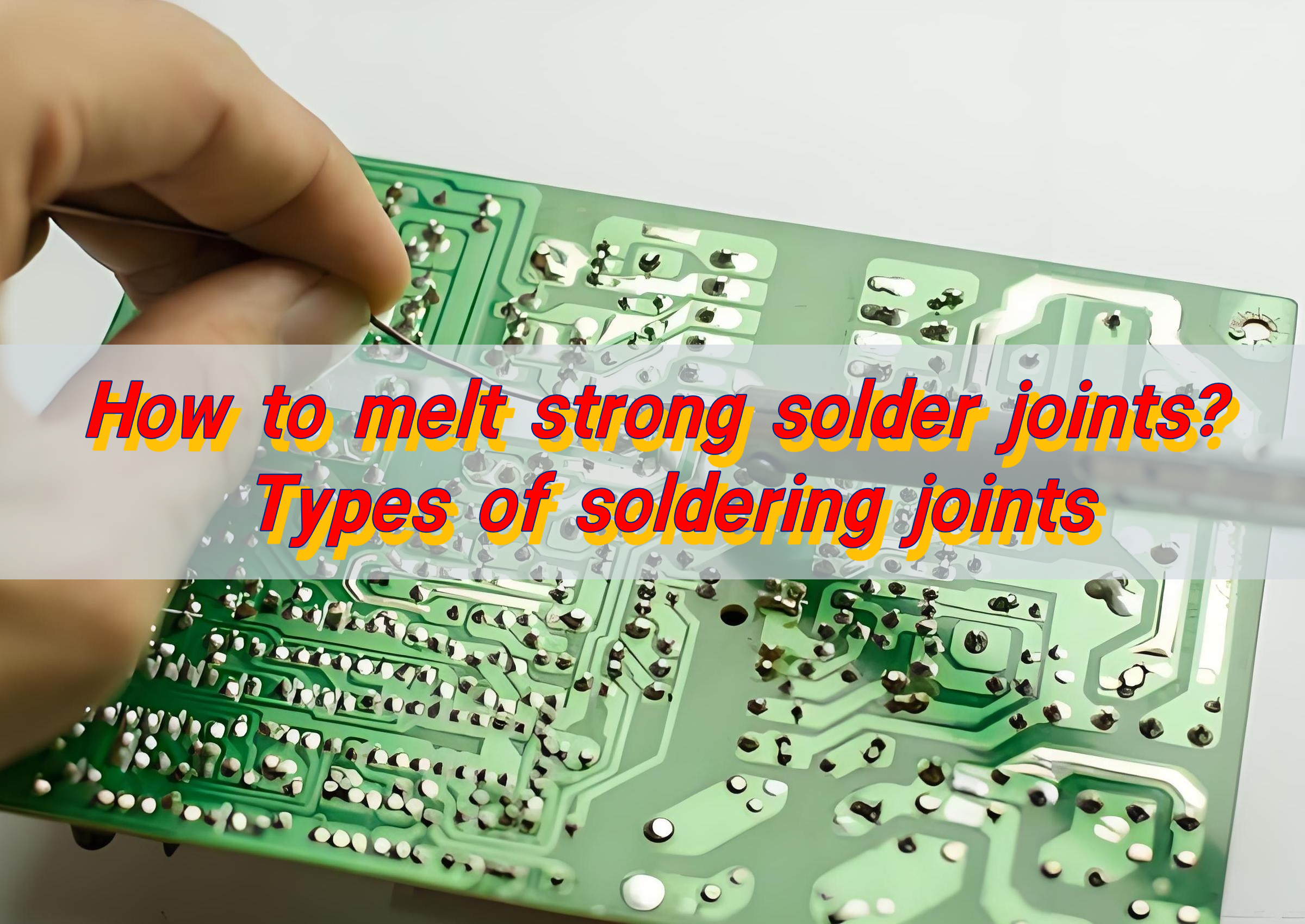
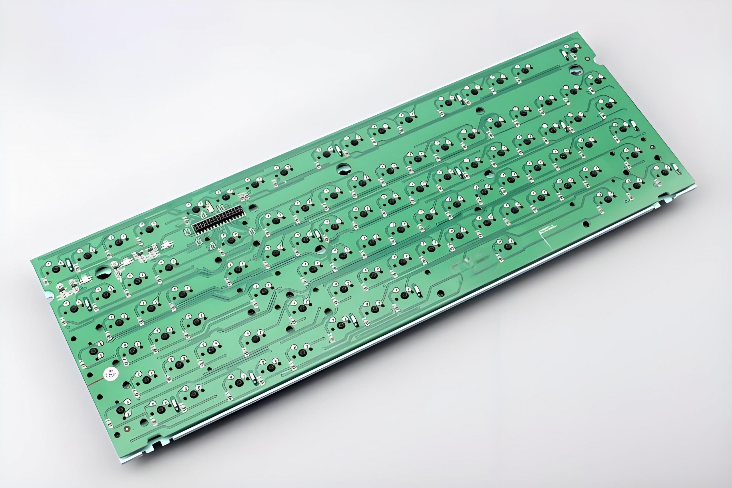
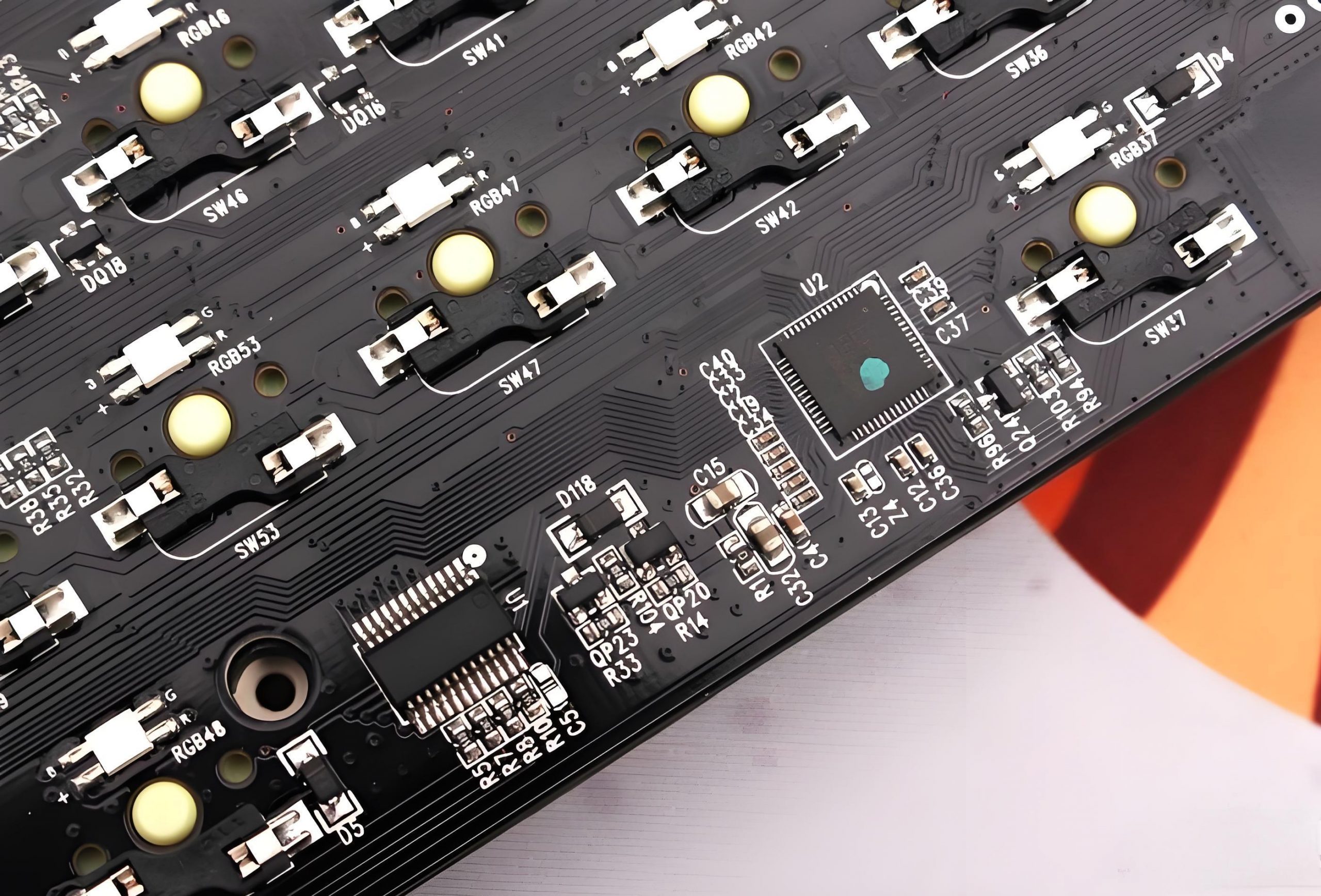
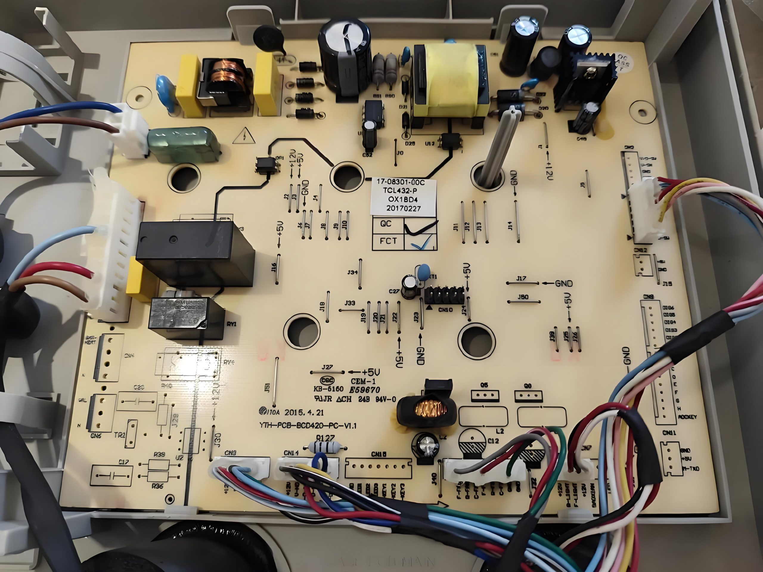
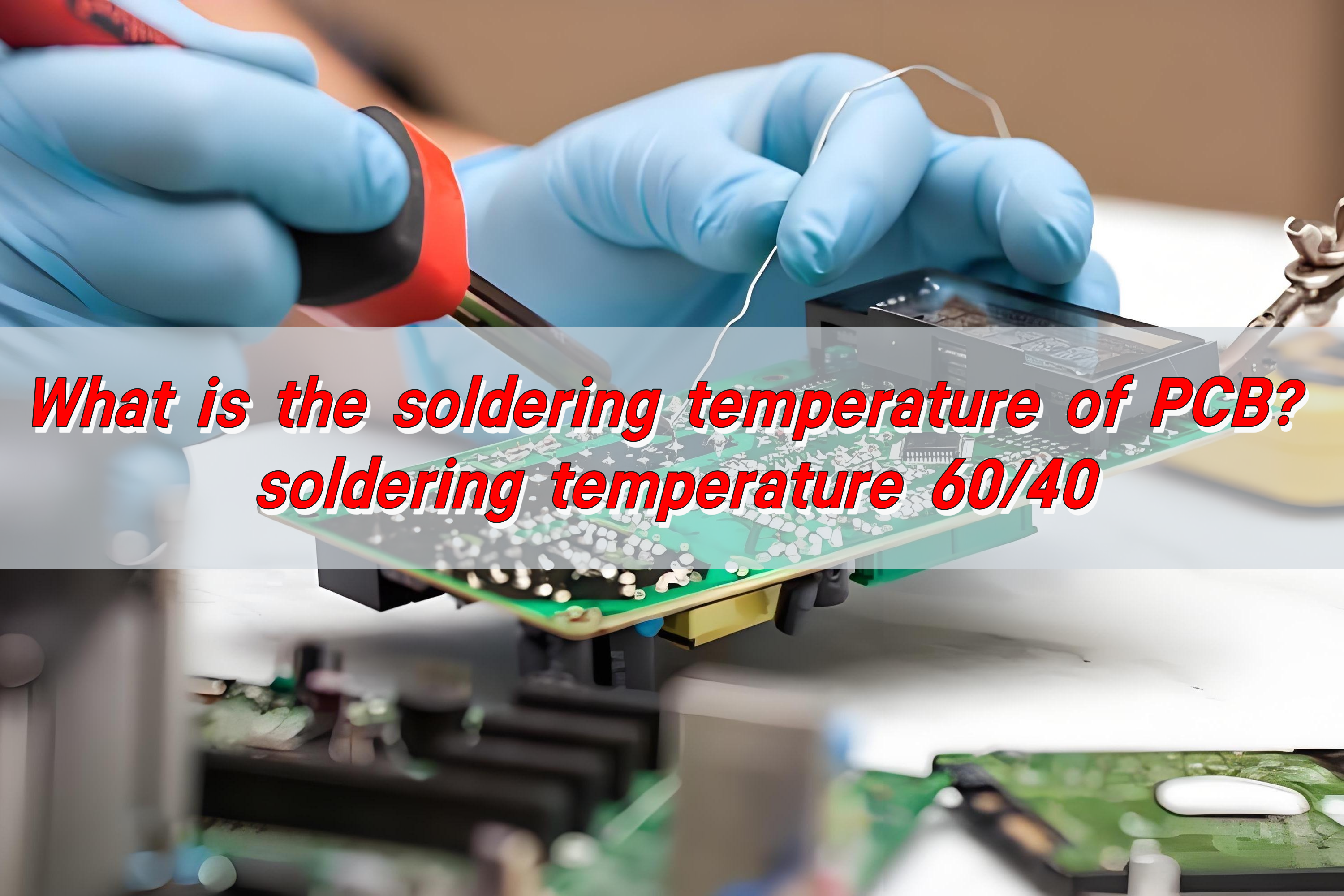
What is the soldering temperature of PCB?When using traditional tin-lead solder, the soldering temperature is roughly in the range of 183℃ – 327℃. For common tin-silver-copper alloys, the melting point is usually in the range of 217℃ – 227℃. During the soldering operation, the temperature is mostly controlled at around 250℃ – 300℃ to ensure that the solder is fully melted and a high-quality solder joint is formed.
What is the best temperature to solder at?
The optimal temperature range for PCB soldering varies depending on the soldering method.
- Surface mount technology: For surface mount technology (SMT), the soldering temperature is generally between 200-240 degrees Celsius. This soldering method includes hot air ovens and reflow soldering, which is mainly used in modern electronic equipment manufacturing.
- Wave soldering: The soldering temperature of wave soldering is generally between 230-260 degrees Celsius. The preheating zone temperature of the wave soldering machine is usually 90-130℃, the solder temperature is 275℃~300℃, the immersion speed is 20mm/s~25mm/s, and the immersion time is 1s~3s.
- Manual soldering: The temperature requirements for manual soldering are relatively high, usually set between 300℃ – 350℃. For precision components such as IC and SMD, it is recommended to control it at 260℃ – 300℃.
- Reflow soldering: The preheating zone temperature of reflow soldering is heated from room temperature to 150℃ – 200℃, the wetting zone is maintained at 150℃ – 200℃, and the peak temperature of the reflow zone is 230℃ – 260℃. The entire reflow soldering process is usually controlled within 4-7 minutes.
- Lead-free solder: For lead-free solder, due to its high melting point, the soldering temperature usually needs to be higher, generally between 250℃ – 280℃.
What temperature is 60 40 soldering?
The optimal soldering temperature range of 60/40 solder wire is 220℃-240℃. Within this temperature range, the fluidity and wettability of the solder wire are good, which can ensure the quality and effect of soldering components.
In addition, different types of solder wire have different optimal temperature ranges:
- 63/37 alloy: high melting point, suitable for soldering circuits and PCB boards, the optimal temperature range is 260℃-280℃.
- 55/45 alloy: melting point is 187℃-202℃, suitable for specific application scenarios.
- 50/50 alloy: melting point is 190℃-216℃, suitable for soldering tasks requiring higher melting points.
- 45/55 alloy: melting point is 192℃-227℃, suitable for soldering tasks requiring higher melting points.
- 40/60 alloy: melting point is 194℃-238℃, suitable for specific high melting point soldering needs.
- 35/65 alloy: melting point is 198℃-247℃, suitable for high melting point welding tasks.
- 30/70 alloy: melting point is 202℃-256℃, suitable for extremely high melting point welding tasks.
What is too much heat on solder?
Overheating of PCB solder can lead to a variety of problems, including reduced soldering quality, component damage and safety hazards. Specifically:
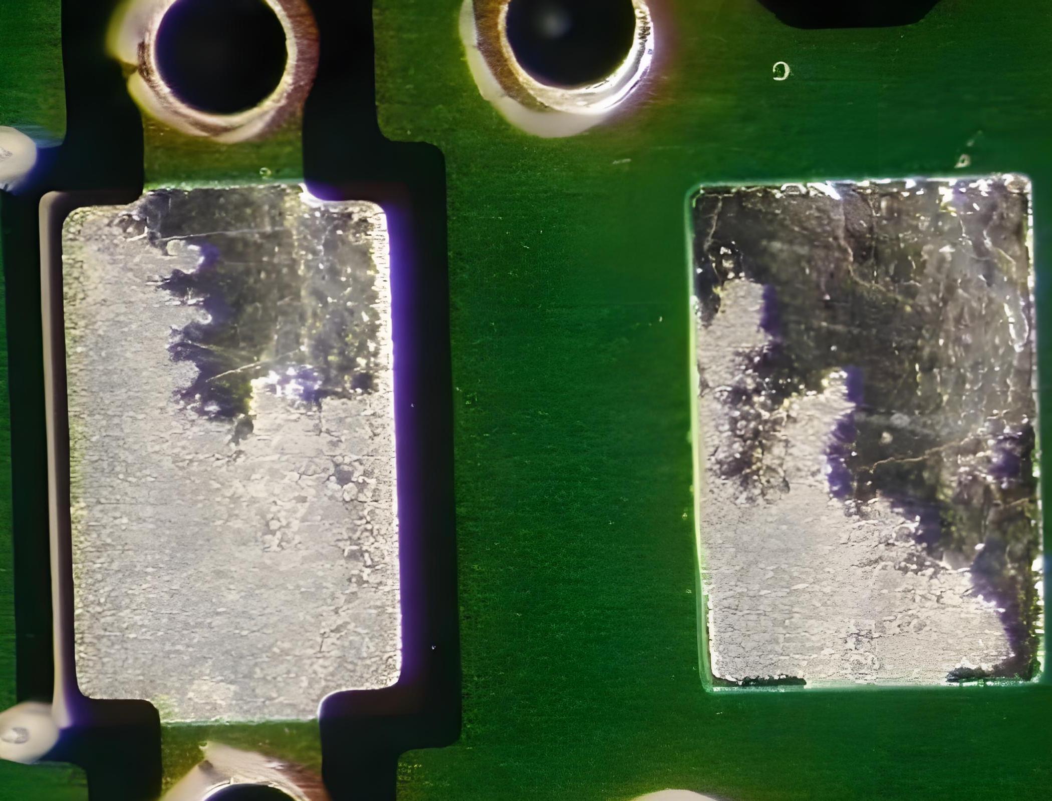
- Degraded soldering quality: Overheating can lead to increased solder fluidity, which may cause excessive solder joints or solder accumulation, affecting soldering quality. In addition, overheating may also cause solder joints to turn white, have no metallic luster, have a rough surface, easily peel off, and reduce strength.
- Component damage: High temperature accelerates the aging process of electronic components and shortens their life. Long-term overheating may cause damage, burning or failure of electronic components, requiring more frequent component replacement, and increasing repair and maintenance costs.
- Safety hazards: Overheating may cause fire risks. In extreme cases, overheated PCB boards may cause wires, cables and other materials to melt, causing fires.
Do and don’ts of soldering?
The precautions for PCB soldering include the following aspects:
1. Selection of soldering materials and flux:
- Soldering materials: Commonly used soldering materials include tin-lead solder, which is suitable for general electronic product assembly due to its low melting point, high mechanical strength, low surface tension, and good oxidation resistance.
- Flux: Flux is divided into solder resist and soldering flux. The soldering flux is mainly used to remove oxide film, prevent oxidation, reduce surface tension, and increase solder fluidity. Commonly used soldering fluxes include rosin series, which are non-corrosive and suitable for electronic assembly soldering.
2. Key points of welding technology:
- Surface treatment of weldment: Remove rust, oil, dust and other impurities on the welding surface.
- Pre-soldering: Pre-moisten the welding parts of component leads or wires with solder to reduce welding errors.
- Appropriate amount of flux: Rosin water should only wet the solder joints to be formed to avoid excessive use resulting in excessive solder joints or cold solder joints.
- Keep the soldering tip clean: The soldering tip needs to be cleaned regularly to prevent oxidation from affecting the heating effect.
3. Control of welding temperature and time:
- Temperature control: Too high or too low temperature of the soldering iron will affect the welding quality. It is recommended to use a white light adjustable soldering iron, the temperature is about 350°C for lead soldering, and the temperature is about 380°C for lead-free soldering.
- Time control: Select the appropriate heat and time according to the size and shape of the solder joint to ensure the full melting of the solder and the activation of the active flux.
4. Soldering sequence and component placement:
- Soldering sequence: Prioritize soldering of smaller components, such as resistors and capacitors, and finally solder larger components and connectors.
- Component placement: Components should be neatly, centered, and placed on the board surface, and pay attention to the polarity of the components.
5. Ventilation and safety measures:
- Ventilation: Harmful gases will be generated during welding, and exhaust fans or other ventilation equipment must be equipped.
- Safe operation: Ensure the safety of the operating process, circuit boards and welding tools, and use anti-static tools and protective measures.
What temperature does solder reflow at?
The reflow temperature range of solder during reflow soldering is usually between 220-260℃. Specifically, the four key temperature zones of reflow soldering and their temperatures and times are as follows:
- Preheating zone: The temperature is usually set at 150-200℃ for 60-120 seconds. The purpose of this stage is to preheat the circuit board and components to reduce thermal stress and avoid thermal shock.
- Wetting zone: The temperature range is 180-230℃ for 30-90 seconds. At this stage, the solder paste begins to melt and penetrate into the solder joints, preparing for the next reflow stage.
- Reflow zone: The temperature is usually 220-260℃ for 30-60 seconds. At this stage, the solder paste is completely melted to form a stable solder joint. Too high a temperature or too long a time may cause the solder joint to overheat, while too low or too short a time may cause the solder joint to be loose.
- Cooling zone: The temperature drops below 70℃ for 60-120 seconds. The rapid cooling process helps to reduce the thermal stress of the solder joints and improve the reliability and stability of the product.
In addition, the solder paste will go through four stages during the reflow process: solvent volatilization, oxide removal, melting and reflow, and cooling and solidification. The temperature and time settings of these stages are crucial to ensure the quality of welding and product reliability.
How to remove old solder?
There are mainly the following ways to remove old solder:
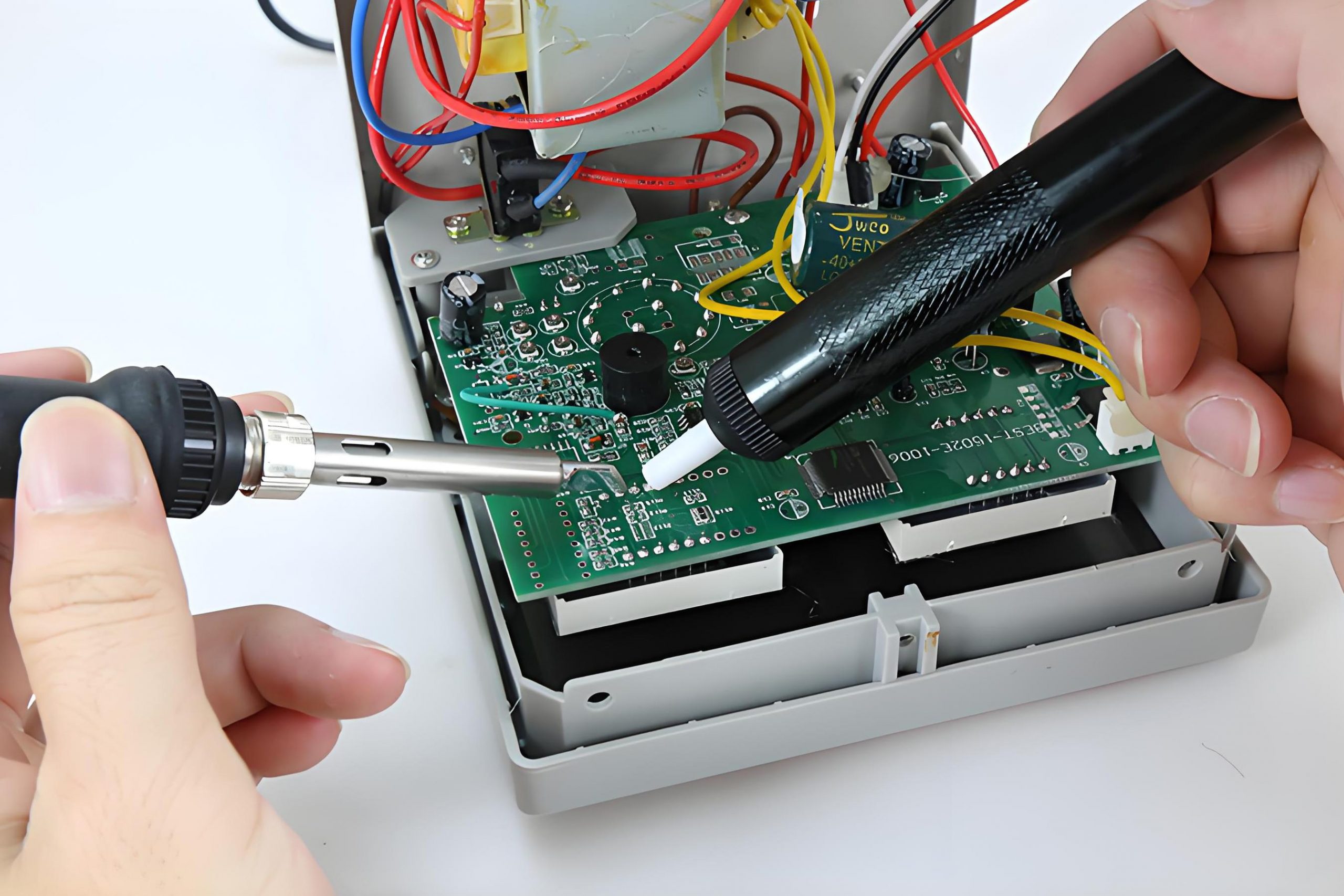
- Use a solder sucker: The solder sucker is a commonly used tool, especially suitable for soldering work on precision circuits. When using a solder sucker, first heat the soldering iron to melt the solder joint, then gently place the solder sucker on the solder joint, and the molten solder will be absorbed by the solder sucker.
- Use anhydrous ethanol or alcohol above 95%: Dip anhydrous ethanol or high-concentration alcohol on a soft brush, brush the solder joint, and then dry it with absorbent cotton.
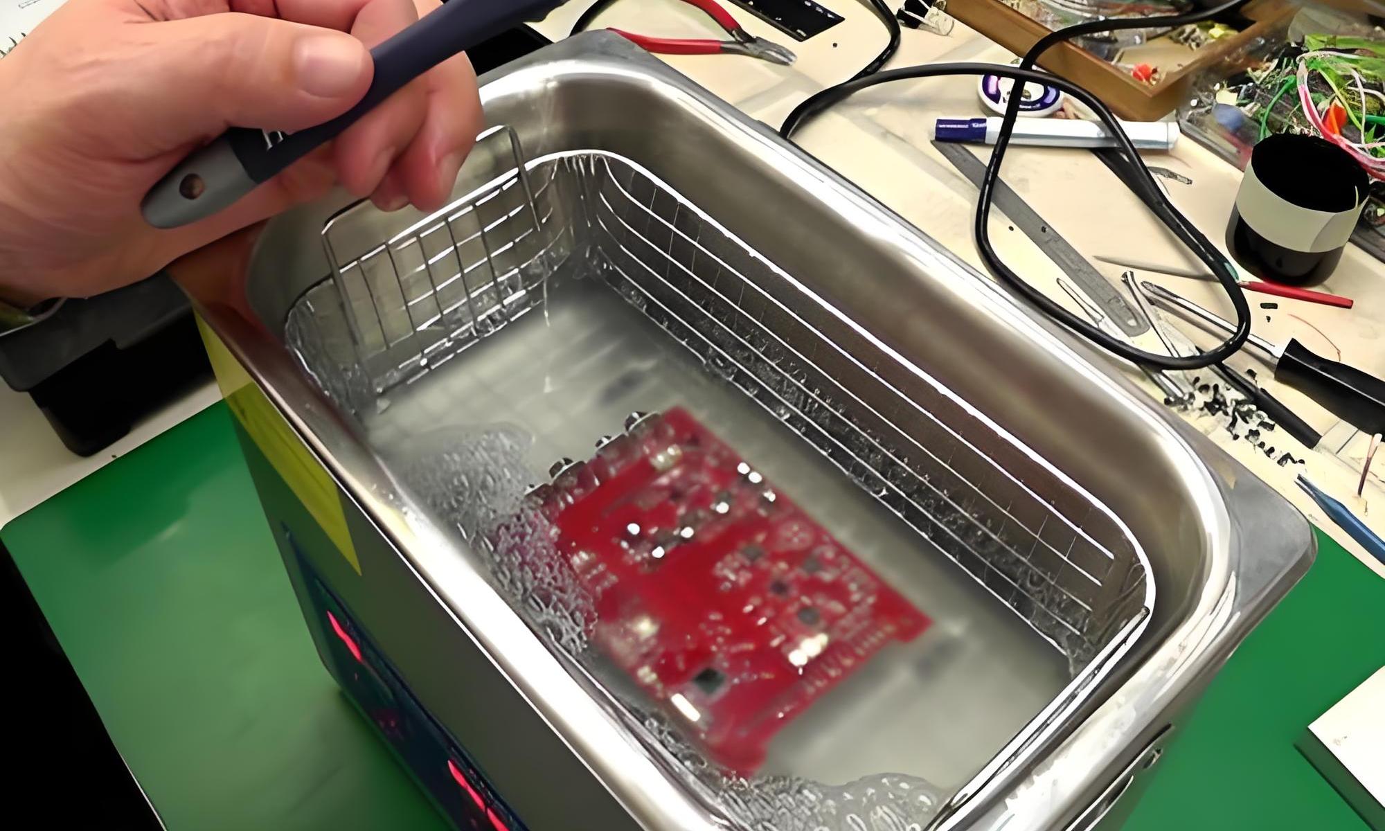
- Ultrasonic cleaning: Ultrasonic cleaning uses the high-frequency oscillation of ultrasound to produce a cavitation effect, which removes the dirt on the solder joint and accelerates the dissolution process of the cleaning fluid.
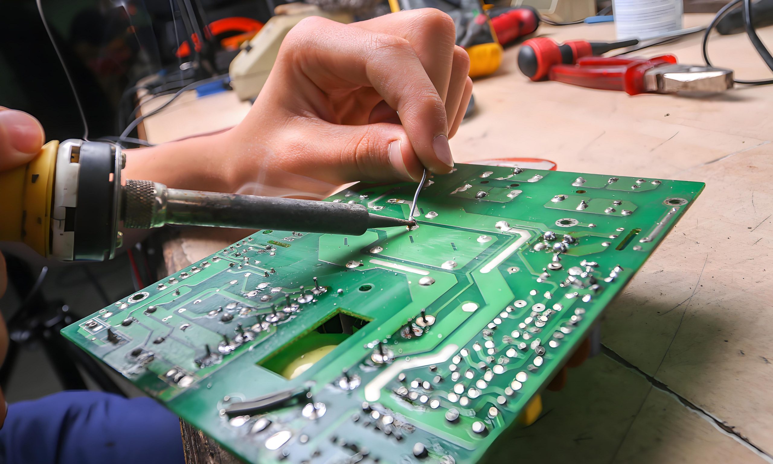
- Manual cleaning: Use manual tools such as tweezers, scrapers, etc. to directly clean the residual solder on the solder joint. This method is simple but inefficient, and it is easy to damage solder joints and components.
- Use special tools: such as desoldering mesh wire, desoldering braided belt, etc. Desoldering mesh wire is made of alloy copper wire and is suitable for removing excess solder on SMT parts solder joints and electronic components of PCB.
In short, the PCB welding temperature is determined by many factors. The melting point of tin-lead solder is 183℃ – 327℃, and the lead-free solder is 217℃ – 227℃; the tools are different, the electric soldering iron solders fine boards at 20 – 30W, 280℃ – 320℃, the hot air gun removes lead chips at 300℃ – 350℃, and the lead-free chips at 380℃ – 420℃. Special scenes are adjusted as needed, and instrument monitoring and calibration are required to ensure the quality of solder joints and products.