How to use AC to DC converter? Let’s explore definition, working principle, using and checking method, assembly processes, expectancy life and cost for AC to DC converter.
Are you troubled with these problems?
- How to balance high power density and low EMI interference in design to avoid certification failure?
- How to achieve rapid PCBA prototyping and multi-version validation during sampling without production delays?
- How to verify PCBA thermal path effectiveness before mass production to prevent bulk performance degradation?
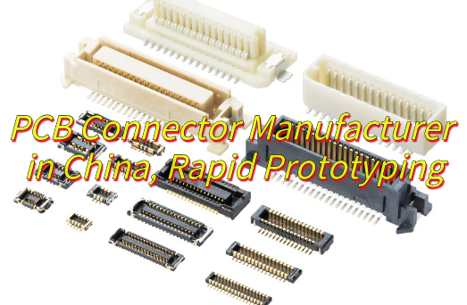
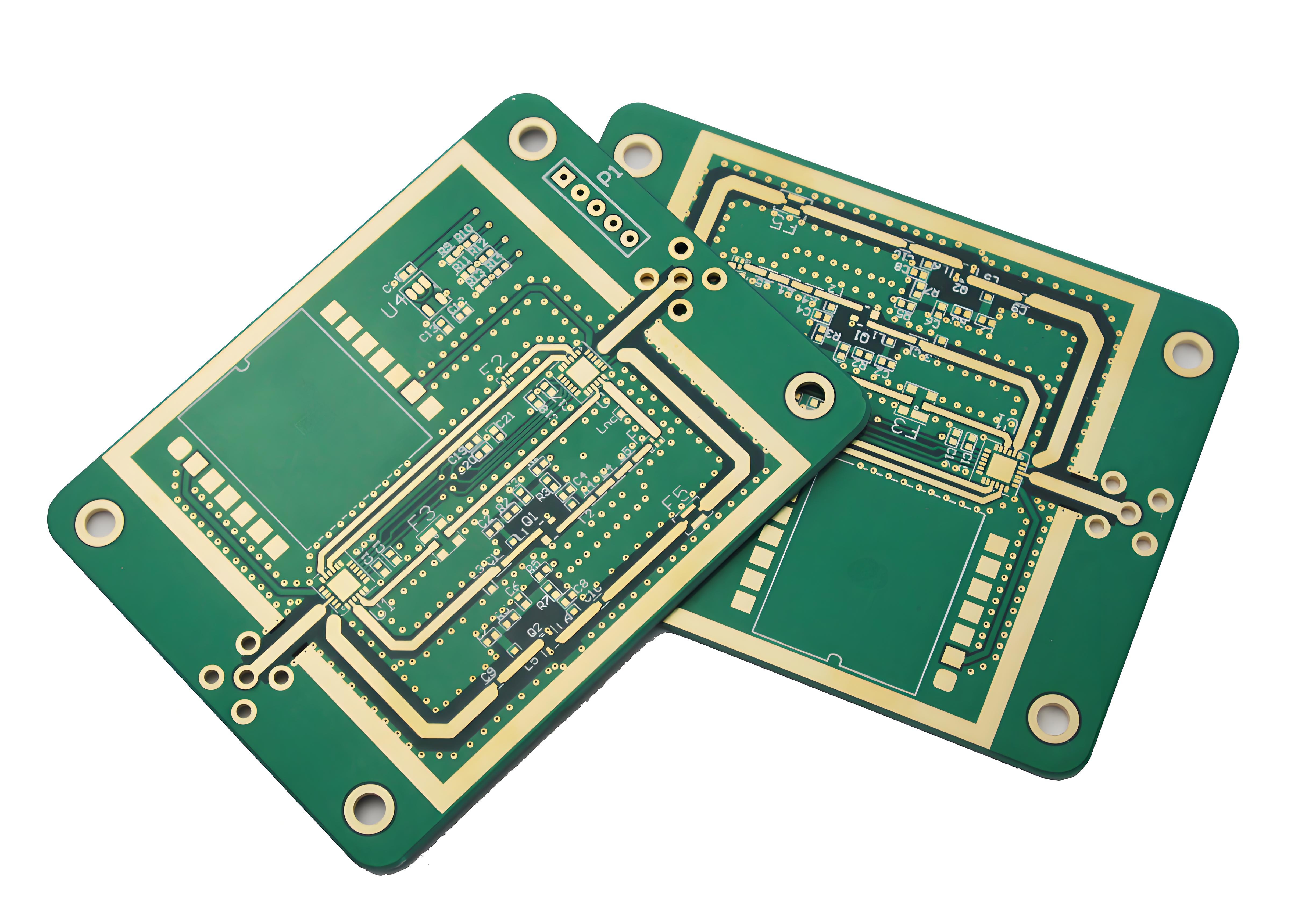
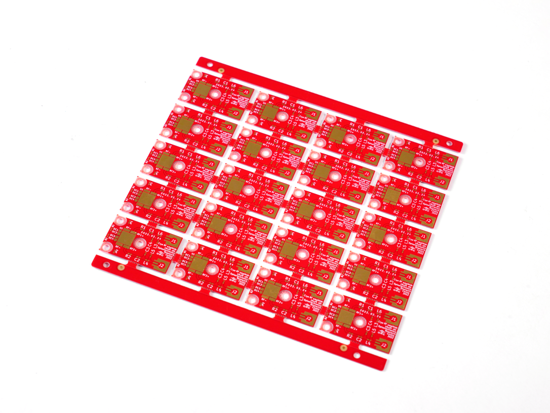
As a AC to DC converter supplier, EBest Circuit (Best Technology) can provide service and solution:
- One-stop design-to-prototyping services via in-house PCBA lines, enabling 48-hour first-article validation with customizable layout optimization.
- Proprietary PCBA thermal simulation & real-world testing alignment technology, offering 3 optimization options during sampling.
- Standardized module library built on PCBA smart manufacturing expertise, enabling flexible small-batch production for multi-model orders with 15% cost reduction.
Welcome to contact us if you have any inquiry for AC to DC converter: sales@bestpcbs.com.
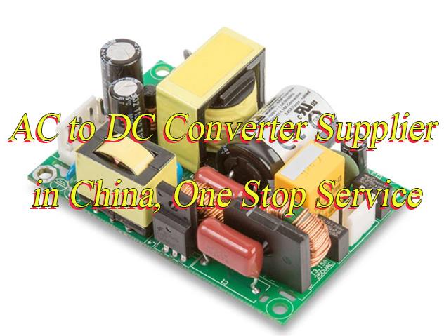
What is an AC to DC Converter Called?
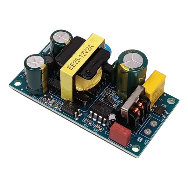
AC to DC Converter (also known as rectifier) is a core device that converts alternating current (AC) into direct current (DC) through rectification, filtering, and voltage regulation circuits. It achieves efficient energy conversion (efficiency can reach 80%-95% or higher, further improved with wide-bandgap semiconductors like GaN/SiC), compact design (reduced size via high-frequency switching technology), and stable output (reduced ripple through capacitors/inductors for sensitive equipment).
Its advantages include high energy efficiency, compact size, and low noise characteristics. It is widely used in consumer electronics (mobile phone/laptop chargers, smart home devices), industrial equipment (motor drives, automation control), renewable energy (photovoltaic inverters, wind power systems), automotive electronics (on-board chargers, electric vehicle V2G technology), and medical/communication fields (medical instruments, base station power supplies).
How Do AC to DC Converters Work?
1. Rectification Stage: AC to Pulsating DC
- Principle: A bridge rectifier circuit (composed of four diodes) performs full-wave rectification, converting 50/60Hz AC into pulsating DC.
- Example: 220V AC is stepped down via a transformer and then rectified by a diode bridge, where both positive and negative half-cycles are conducted to generate a unidirectional pulsating voltage at the load.
- Design consideration: Match the transformer turns ratio to the input voltage to prevent diode reverse breakdown.
2. Filtering Stage: Smoothing Voltage Ripple
- Principle: Low-pass filtering circuits using capacitors or inductors reduce ripple. Capacitors (e.g., electrolytic capacitors) store charge to smooth voltage, while inductors suppress current surges.
- Example: paralleling a high-capacitance capacitor (with voltage rating exceeding peak voltage) at the output can reduce the ripple factor to below 5%.
- Design consideration: In PCB layout, minimize the trace length between capacitors and the rectifier bridge to reduce parasitic inductance.
3. Regulation Stage: Maintaining Stable Output
- Principle: Negative feedback regulation circuits (e.g., linear regulators or switching power supplies) stabilize voltage. Linear regulators adjust transistor voltage drop for low-noise applications, while switching power supplies (e.g., BUCK converters) use PWM modulation and storage inductors for high-efficiency conversion (up to 90%+ efficiency).
- Design consideration: Ensure feedback loop stability to avoid oscillation.
4. Thermal Management: Ensuring Device Reliability
- Principle: Natural/forced air cooling or liquid cooling solutions are employed. For example, high-power AC-DC modules use aluminum heatsinks with thermal grease to lower thermal resistance, coupled with temperature sensors for over-temperature protection.
- Design consideration: Optimize thermal loops in PCB design by placing heat-generating components (e.g., switching transistors) in close contact with heatsinks and avoiding heat source concentration.
5. EMI Suppression: Meeting EMC Standards
- Principle: Input filters (X/Y capacitors + common-mode chokes), shielding techniques (copper foil shielding for transformers), optimized grounding (single-point grounding), and routing rules (avoid loops, shorten high-frequency traces) reduce conducted/radiated noise.
- Example: adding an EMI filter at the input can suppress noise in the 150kHz–30MHz band, complying with IEC 61000-3-2 standards.
How to Use AC to DC Converter?
1. Core Parameter Verification
- Voltage Compatibility Check: Confirm input voltage matches local mains (e.g., 220V in China/120V in the US) and output voltage meets device requirements (5V/12V/24V). Use a multimeter to verify input voltage stability (±15% tolerance).
- Current Redundancy Design: Output current must be ≥120% of device peak demand. For a 2A device, select a converter rated ≥2.4A to prevent overheating.
- Interface Compatibility: Match physical connectors (e.g., USB-C, DC 5.5×2.1mm) and polarity (red=+, black=-). Use adapters if needed—never reverse polarity.
2. Tool & Cable Specifications
- Cable Selection: Input cables must comply with IEC 60320 standards (e.g., C13/C14 plugs) with ≥0.75mm? gauge to avoid overheating. Output cables: 18AWG for ≤10A, 16AWG for ≤20A.
- Safety Gear: Equip with insulated screwdrivers, digital multimeters, and hygrometers. In damp environments, use splash-proof boxes or insulated gloves; outdoor setups require waterproof connectors.
3. Input Power Connection
- Socket Standards: Use GB 2099.1-compliant sockets—avoid damaged/aged outlets. For multi-device sharing, total load must not exceed 80% of socket rating.
- Grounding Protection: Metal-cased devices require reliable grounding. Use RCDs (≤30mA trip current) and add electric field barriers in wet conditions.
4. Output Device Connection
- DC Device Wiring: Strictly follow “positive-to-positive, negative-to-negative” wiring. For parallel connections, use fused splitters with single-branch current ≤80% of converter rating.
- Special Equipment Handling: Motors need flyback diodes; LEDs require series resistors; relays need TVS diodes for surge protection.
5. Power-On Testing & Fault Diagnosis
Initial Verification:
- Measure output voltage with a multimeter (±3% tolerance). Monitor device indicators and cooling fan operation.
Troubleshooting:
- No output: Check input fuses, short/open circuits.
- Low voltage: Verify input stability, capacitor aging, or overload.
- Overheating: Disconnect power, check cooling, and confirm load ≤80% of rating.
6. Daily Use & Maintenance
- Environmental Control: Operate within -10°C to 40°C, ≤85% RH. Avoid direct sunlight, dust, or corrosive gases.
- Maintenance Schedule: Clean heat sinks quarterly; tighten terminals. Annual insulation tests (≥20MΩ).
- Storage & Transport: Secure cables during transit; store in dry, ventilated areas away from corrosives.
7. Safety & Emergency Protocols
- Protection Features: Ensure OCP/OVP/OTP protection. Prefer hiccup-mode converters for auto-recovery after faults.
- Fire Response: Cut power immediately if smoke/odor occurs. Use dry powder extinguishers—never water.
- Child Safety: Use locked sockets or safety covers; place converters out of reach.
8. Special Application Scenarios
- International Travel: Use wide-input (100-240V) converters with region-specific plug adapters (e.g., Japan 100V).
- Industrial Use: Select IEC 61000-4-compliant units with EMI/surge resistance. Add dust covers in high-particulate environments.
- Medical Devices: Use IEC 60601-1-certified medical-grade converters with dual power supplies and failure alarms.
9. Efficiency Optimization
- Energy Efficiency Tiers: Tier 1 (≥98%) for full-load; Tier 2 (≥96%) for standard; Tier 3 (≥94%) for intermittent use.
- Hybrid Control Modes: Enable PFM/PWM switching, PFM for light loads (reduced switching loss), PWM for heavy loads (higher efficiency).
- Cooling Solutions: Passive cooling for ≤50W; forced air for 50-200W; liquid cooling for >200W.
How to Check If an AC to DC is Working?
1. Input Power Verification
- Plug Contact Check: Use multimeter continuity mode to measure plug-to-socket contact resistance (≤0.5Ω) to prevent voltage drop.
- Voltage Range Validation: Record mains voltage fluctuation (e.g., 220V±10% = 198-242V) and confirm device input specification coverage (e.g., 100-240V).
- Grounding Integrity: Measure PE (ground) to chassis resistance (≤0.1Ω) for effective earth protection.
2. No-Load Voltage Test
- Dynamic Compensation: Document open-circuit voltage deviation (e.g., ±2% for 12V adapter) with temperature coefficient (-0.03V/℃) for cold-state compliance.
- Load Effect Analysis: After no-load measurement, apply 10% load to observe voltage change (≤±3%) to eliminate false readings from uncharged capacitors.
3. Load Voltage Stability Test
- Dummy Load Configuration: Select power resistor matching adapter rating (e.g., 12Ω/15W for 12V/1200mA) with four-wire measurement to eliminate lead resistance errors.
- Dynamic Monitoring: Use oscilloscope to capture voltage transient response time (≤20ms) during 50%-100% load step, ensuring no oscillation/overshoot.
4. Load Transient Response Test
- Step Loading: Increment load by 20% steps, recording voltage at each stable point to plot load-voltage curve (linearity slope ≤0.1V/A).
- Protection Calibration: Test overcurrent protection at 150% rated current, documenting activation delay (≤500ms) to prevent false/delayed tripping.
5. Protection Function Validation
- Overcurrent Test: Simulate short-circuit with electronic load to verify output cutoff within 10ms and recovery method (manual/auto reset).
- Overvoltage Test: Gradually increase input voltage to determine OVP threshold (e.g., 264V shutdown) requiring power-cycle restart.
6. Physical Inspection
- Cable Aging: Measure cable tensile strength (≥50N) and insulation temperature rating (e.g., 85°C) for environmental compatibility.
- Thermal Design: Verify heatsink-to-component contact pressure (≥30kPa) and thermal paste integrity (no cracking/missing).
7. Component Inspection
- Capacitor Evaluation: Use LCR meter to measure capacitance tolerance (±20%) and ESR (≤1.5× rated) for aging assessment.
- Chip Temperature: Scan regulator chip surface with thermal imager (≤125°C) during full load, cross-referencing derating curves.
8. Efficiency & Thermal Test
- Power Measurement: Calculate efficiency η=(P_out/P_in)×100% using power meter (input) and electronic load (output).
- Thermal Gradient: Record temperature rise curve (max ΔT≤40°C after 30min) with thermal equilibrium time (≤20min).
9. Waveform & Noise Analysis
- Ripple Measurement: Set oscilloscope bandwidth (20MHz), probe ×10 attenuation, and 5ms/div timebase to measure output ripple (e.g., ≤50mVp-p for 12V).
- EMI Compliance: Use spectrum analyzer for conducted noise (150kHz-30MHz ≤EN55022 Class B) and radiated noise (30MHz-1GHz ≤40dBμV/m).
10. Compatibility & Long-Term Stability
- Voltage Adaptability: Perform full-load tests at 180V/220V/250V input to verify voltage variation (≤±2%).
- Aging Test: Conduct 8-hour continuous operation, monitoring hourly voltage drift (≤±0.1V) and capacitance change (≤±5%) for performance stability.
How to Build AC to DC Converter?
1. Select an Appropriate Transformer
- Choose a step-down transformer based on target output voltage and current. For example, converting 220V AC to 12V DC requires a transformer with rated power ≥ load demand to prevent overload burnout.
2. Design the Rectifier Circuit
- Use a bridge rectifier (e.g., four 1N4007 diodes forming a rectifier bridge) to convert AC into pulsating DC. This utilizes both positive and negative half-cycles, offering higher efficiency than half-wave rectification.
3. Configure the Filter Capacitor
- Parallel a large-capacity electrolytic capacitor (e.g., 2200μF/25V) at the rectifier output to filter low-frequency ripple. The capacitor’s voltage rating must ≥ peak input voltage (e.g., 220V AC peak ≈ 311V) to avoid breakdown.
4. Build the Voltage Stabilization Circuit
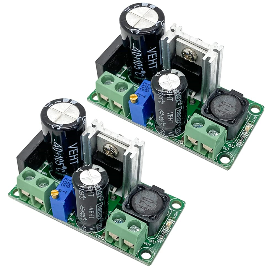
- Adopt linear regulators (e.g., 7805) or switching regulator modules (e.g., LM2596) to stabilize output voltage. Linear regulators suit low-power scenarios, while switching regulators offer higher efficiency for high-current demands.
5. Implement Safety Protection Measures
- Add a fuse (rated current slightly above operating current) to prevent short circuits.
- Install varistors or gas discharge tubes to suppress surge voltages.
- Equip output terminals with TVS diodes to protect loads from transient high-voltage damage.
6. Optimize Heat Dissipation
- Equip heat-generating components (e.g., transformers, rectifier bridges, regulator chips) with heat sinks or forced air cooling. Aluminum heat sinks should make tight contact with components, enhanced by thermal silicone grease.
7. Optimize Circuit Layout
- Keep high-frequency noise-sensitive lines (e.g., feedback loops) away from high-current paths.
- Use star grounding for input/output terminals to avoid ground loop interference.
- Employ shielded wires or ferrite beads to suppress EMI.
8. Test and Debug
- Measure node voltages with a multimeter to confirm rectified voltage is √2 times input voltage (e.g., 220V AC rectified ≈ 311V DC).
- Conduct load testing by gradually increasing current while monitoring output stability and component temperature rise.
- Use an oscilloscope to verify ripple voltage ≤ 5% of output voltage.
9. Package and Insulate
- Wrap all exposed conductors with heat-shrink tubing or insulating paint. Use high-temperature, flame-retardant materials for terminals. Metal enclosures must be reliably grounded and comply with electrical safety standards (e.g., 3C certification).
10. Efficiency Optimization
- Switching power supply schemes can reduce magnetic component size by increasing switching frequency (e.g., >100kHz). Synchronous rectification lowers diode voltage drop losses, boosting overall conversion efficiency >90%.
What Is the Life Expectancy of an AC to DC Converter?
The lifespan of AC to DC converters is influenced by dynamic factors rather than a fixed duration. High-quality units in ideal conditions can last over 10 years, with potential extensions to 15 years through proper maintenance.
Component types significantly affect durability, such as electrolytic capacitors being sensitive to voltage and temperature, while solid-state components like MOSFETs require effective heat dissipation. Environmental factors like sustained high temperatures, humidity, and voltage fluctuations accelerate aging.
Usage patterns also matter, continuous full-load operation generates more heat compared to intermittent use, and maintaining 70%-80% rated power improves longevity. Regular parameter monitoring, adequate ventilation, and avoiding extreme storage environments further enhance reliability.
How Much Does AC to DC Converter Cost?
The cost of an AC/DC converter varies depending on power capacity, output current, brand reputation, and quality standards, with prices typically quoted in US dollars. For example, a low-power adapter (e.g., 500mA) may range from $7 to $11, a mid-range model (12V/5A) typically costs between $30 and $130, and a high-power industrial adapter (50A) can cost over $170.
Technical specifications also influence pricing, features such as universal voltage input (110-240V), integrated power factor correction (PFC), or programmable functionality often increase costs. Other factors, such as custom design requirements, thermal management efficiency, and brand premiums, further extend the price range, from a few dollars to several hundred dollars. Accurate cost assessment requires evaluating specific application requirements, including environmental conditions and expected service life, to effectively balance performance and budget.
Why Choose EBest Circuit (Best Technology) as AC to DC Converter Supplier?
Reasons why choose us as AC to DC converter supplier:
- Price Competitiveness: Achieve cost-sensitive solutions through design optimization and large-scale procurement, such as adopting high-cost-performance component alternatives and centralized bulk material procurement, reducing overall customer costs by 15%-20% while providing tiered pricing systems for different order volumes.
- Emergency Order Response: Establish dedicated rapid channels to complete full-process proofing from design verification to sample delivery within 24 hours, equipped with dual-shift engineering teams and automated testing equipment, ensuring rapid closure of R&D issues and shortening product launch cycles by over 30%.
- On-Time Delivery Guarantee: Rely on intelligent production scheduling systems and dynamic logistics monitoring to achieve a 99.2% on-time delivery rate, utilizing real-time production dashboards and supply chain collaboration platforms to proactively alert potential delays and provide alternative solutions, ensuring uninterrupted customer production plans.
- Comprehensive Quality Control: Implement a four-stage inspection system from raw material incoming inspection to final product shipment, including AOI optical inspection, X-RAY, environmental stress screening, and final functional testing. Each batch undergoes 100% full inspection with attached test reports, ensuring defect rates below 0.05%.
- One-Stop Solution: Integrate EDA toolchains and smart factory resources to provide full-process services from conceptual design, PCB layout, prototype manufacturing, mass production, to logistics distribution. Customers only need to interface with a single point of contact to manage the entire project lifecycle.
- Technical Support Services: Equipped with a senior engineering team with 15 years of experience, offering 7×24 online technical support including circuit design optimization suggestions, failure analysis report generation, EMC/EMI rectification solutions, assisting customers in overcoming technical challenges and enhancing product performance.
- Customized Design Capability: Based on modular design platforms supporting parametric customization, quickly adjust key parameters such as output voltage, power density, and package size to adapt to special requirements across 20+ niche fields including industrial control, medical equipment, and new energy vehicles, achieving 48-hour rapid prototype delivery.
- After-Sales Rapid Response: Establish a three-tier service system, 48-hour remote diagnostics for routine issues, 72-hour on-site engineer dispatch for complex faults, and annual maintenance plans with spare parts inventory management services, reducing customer after-sales costs by over 20%.
Welcome to contact us if you have any request for AC to DC converter: sales@bestpcbs.com.