In the vast field of materials science, copper occupies an important position with its excellent performance. Among them, the thermal conductivity of copper is particularly eye-catching, becoming the preferred material for heat conduction in many fields. Copper plays an important role in electronic equipment, heat exchangers, construction and other fields.
What is the thermal conductivity value for copper?
The thermal conductivity of copper is about 401W/m·K.
The thermal conductivity refers to the heat transferred through 1 square meter of area in 1 second under stable heat transfer conditions, with a temperature difference of 1 degree (K, ℃) on both sides of a 1 meter thick material. The unit is watt/meter·degree (W/(m·K)).
The thermal conductivity is a parameter to measure the thermal conductivity of a material. The larger the value, the better the thermal conductivity. Due to its high thermal conductivity, copper is often used to make radiators, heat conductors and other applications that require efficient heat transfer.
What is the thermal conductivity of copper at 25 C?
The thermal conductivity of copper is affected by many factors. On the one hand, temperature is an important influencing factor. Generally speaking, the thermal conductivity of copper decreases with increasing temperature.
At 25℃, the thermal conductivity of copper is about 401W/m.K, and at 100℃, the thermal conductivity of copper is 377W/m・K.
How do you measure thermal conductivity of copper?
The thermal conductivity of copper is usually measured by the steady-state method.
The steady-state method is a classic method for measuring the thermal conductivity of thermal insulation materials. It uses the equilibrium state in which the heat transfer rate is equal to the heat dissipation rate during stable heat transfer.
This method has a simple and clear principle and high accuracy. Although the measurement time is long and the environmental conditions are high, it is suitable for measuring thermal conductivity materials at medium temperatures, especially for low thermal conductivity materials such as rock, plastic, rubber, glass, and thermal insulation materials.
In the steady-state method, commonly used methods include heat flow method, protected heat flow method, and protected hot plate method. The basic principles of these methods are similar, but some standards are formulated for different thermal insulation materials, and the test results are similar.
What metal has the highest thermal conductivity?
Silver has the highest thermal conductivity.
Among metals, silver has a thermal conductivity of 411W/(m·K), which is the highest value among all metals. This property of silver makes it the metal with the best thermal conductivity.
In contrast, copper has a thermal conductivity of 401W/(m·K), which is also very high, but still slightly lower than silver. Other metals such as gold and aluminum have thermal conductivities of 315W/(m·K) and 237W/(m·K), respectively, which are lower than silver and copper. Therefore, from the perspective of thermal conductivity, silver is undoubtedly the metal with the best thermal conductivity.
In addition, although the thermal conductivity of copper is also very high, reaching 401W/(m·K), second only to silver, among pure metals, the thermal conductivity of silver is still the highest. However, in practical applications, copper is widely used because of its good conductivity and relatively low cost.
Which metal is the poorest conductor of heat?
The metal with the worst thermal conductivity is iron.
Among metal materials, the thermal conductivity of iron is 0.163, while that of copper and silver is, and that of aluminum is 0.5. These data indicate that the thermal conductivity of iron is significantly lower than that of other common metals. Therefore, it can be concluded that iron is the metal with the worst thermal conductivity.
Why copper has highest thermal conductivity?
Copper has the highest thermal conductivity, mainly because of its unique physical and chemical properties. The superior thermal conductivity of copper is mainly attributed to its crystal structure and electronic properties.
Copper is a metal with good electrical and thermal conductivity, which is due to the presence of a large number of free electrons in the crystals of copper. These free electrons can effectively transfer heat when colliding with metal cations in the crystal, making copper extremely thermally conductive.
The thermal conductivity of copper is about 400 W/m·K, which means that copper transfers much more heat per unit time than most other materials. The high thermal conductivity allows copper to quickly transfer heat away, with efficient heat dissipation.
What happens to copper when it is heated?
When copper is heated, its volume increases, its mass remains unchanged, and its density decreases.
When copper is heated, its volume increases due to the property of thermal expansion and contraction. This is because when the copper block is heated, the distance between atoms increases, resulting in an increase in volume. At the same time, the mass of copper is a property of matter, which is only related to the amount of matter contained, and has nothing to do with the position, state, shape, and temperature of the object. Therefore, the mass of copper remains unchanged after heating.
In addition, when copper is heated in the air, if it reacts with oxygen, black copper oxide (CuO) will be generated on the surface. This chemical change will cause the color of copper to change from red to black.
In summary, when copper is heated, not only will its volume increase, its mass remain unchanged, and its density decrease, but it will also react with oxygen to generate copper oxide when heated in the air, resulting in a change in surface color.
Why does copper turn green?
Copper turns green because it is oxidized in the air to form copper rust. The main component of this copper rust is basic copper carbonate, which is green in color.
Copper will be oxidized in the air to form copper rust. This rusting process is the result of a combination of factors, including the reaction of copper with oxygen, water vapor and carbon dioxide in the air.
Specifically, when copper is exposed to oxygen, water and carbon dioxide in humid air for a long time, a chemical reaction will occur to generate basic copper carbonate (Cu2(OH)2CO3), a green inorganic compound, so a green rust layer will form on the copper surface.
This process not only occurs on the surface of copper, but also because the main component of copper rust is basic copper carbonate, the color of copper rust is green, which makes the appearance of copper products appear green.
Copper has become the preferred material for heat conduction in many fields due to its high thermal conductivity, good processing performance and stable thermal conductivity. With the continuous advancement of science and technology, it is believed that copper will continue to play an important role in future development.
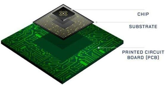
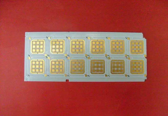
IC substrates are usually made of multiple layers of insulating materials, conductors, and semiconductor materials. These materials are precisely processed to form a complex circuit network. The material selection of the substrate has a crucial impact on its performance, such as thermal conductivity, electrical properties, mechanical strength, etc.
IC substrates play an important role in electronic devices, providing stable support and efficient connections for integrated circuits. With the continuous development of electronic technology, the importance of IC substrates will continue to increase.
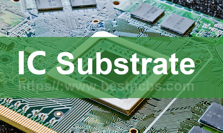
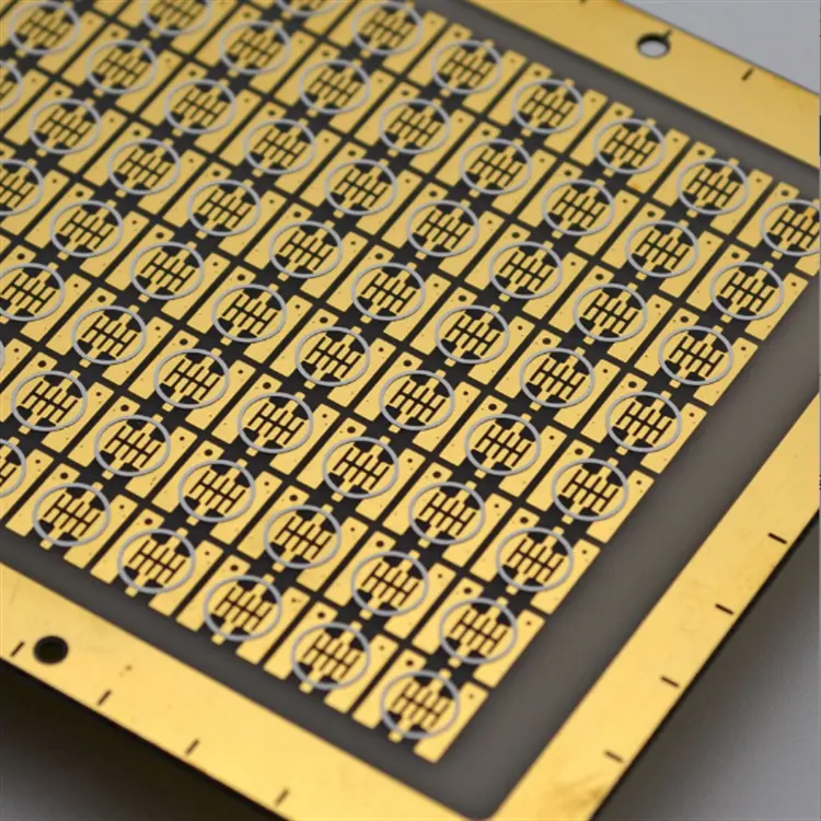
What is an ic substrate
IC substrate, also known as ic package substrate, is a substrate used to package bare IC (integrated circuit) chips. It is the core material of chip packaging and has the characteristics of high density, high precision, high performance, miniaturization and thinness.
As an intermediate product, IC substrate connects the chip and the circuit board, plays a role in physical mechanical support, heat dissipation and protection, and provides electronic connection between the chip and the PCB to achieve signal transmission.
It is a key carrier in the packaging and testing process and is widely used in mainstream packaging technologies such as BGA (ball grid array packaging) and CSP (chip size packaging). The main functions of the packaging method include isolating the exposed chip from the air, preventing corrosion of the circuit on the chip, and providing an intermediate bridge for information transmission between highly refined chips and less refined printed circuit boards.
IC substrate definition
IC substrate is the support of semiconductor integrated circuits. Its main function is to connect various electronic components to form a complete circuit system. As a platform, it provides a solid foundation for various components within the IC to ensure the normal operation of the circuit.
IC substrate manufacturing process
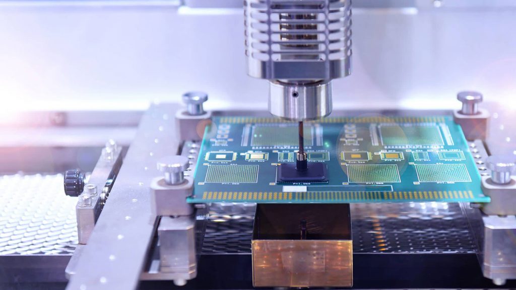
How are ic substrates made? IC (Integrated Circuit) substrate manufacturing refers to packaging electronic components onto a circuit board to form a complete circuit system. The IC substrate manufacturing process mainly includes the following steps: design, proofing, printing, drilling, gold plating, welding, testing and packaging.
Design, schematic design and layout design are carried out according to the circuit design requirements, the size and number of layers of the circuit board are determined, and process analysis is carried out to determine the substrate manufacturing process.
Proofing, the designed circuit board sample is generated into a file, and the graphics on the file are transferred to the circuit board through a photolithography machine to form a copper pole, etc.
Printing, the area on the circuit board on the graphics transferred by the photolithography machine is etched to remove unnecessary copper and expose the glass fiber surface.
Drilling, use a drilling machine to make the required holes on the circuit board for welding components.
Gold plating, a layer of metal is covered on the surface of the circuit board through the electroplating process, which can improve the conductivity of the product on the one hand and prevent oxidation on the other hand.
Soldering: solder IC chips and other components to the corresponding positions of the circuit board, using hot plates and brackets for soldering.
Testing: test the soldered circuit board to verify whether the electrical performance, signal path and stability of the circuit board meet the design requirements.
Packaging: label, clean and package the qualified circuit boards to make them suitable for transportation and storage.
how ic substrate differentiate? The IC substrate manufacturing process is a complex and delicate process that requires a series of steps such as design, proofing, printing, drilling, gold plating, welding, testing and packaging. Only by strictly following the process can the quality and performance of the final product be guaranteed.
IC substrate manufacturers
As a leader of IC substrate manufacturer, EBest Circuit (Best Technology) has over 18 years experience, we are so confident that we can provide the highest quality and high specifition IC substrate for you! Backing up with a group of professional engineers, and well established quality system. EBest Circuit (Best Technology) has grown to become a major PCB manufacturer in Asia to serve in diverse customers base. At EBest Circuit (Best Technology), you can enjoy a full turn-key service from IC substrate design, prototyping, mass production and IC substrate assembly.
IC substrate manufacturers
How ic substrate differentiate
How to distinguish IC substrates? The distinction of IC substrates can be made in many ways, mainly including classification by package type, material properties, and bonding technology.
1. Classification by package type:
BGA IC substrate: It performs well in heat dissipation and electrical performance, can significantly increase chip pins, and is suitable for IC packages with more than 300 pins.
CSP IC substrate: It is a single-chip package with light weight, small size, and similar size to IC. It is mainly used in memory products, telecommunications products, and electronic products with a small number of pins.
FC IC substrate: By flipping the chip package, it has low signal interference, low circuit loss, good performance, and effective heat dissipation.
MCM IC substrate: It absorbs chips with different functions into one package, which is light, thin, short, and miniaturized, but because multiple chips are packaged in one package, this type of substrate does not perform well in signal interference, heat dissipation, fine wiring, etc.
2. Classification by material properties:
Rigid IC substrate: Mainly made of epoxy resin, BT resin or ABF resin, with a CTE (coefficient of thermal expansion) of about 13 to 17ppm/°C.
Flex IC substrate: Mainly made of PI or PE resin, with a CTE of 13 to 27ppm/°C.
Ceramic IC substrate: Mainly made of ceramic materials such as alumina, aluminum nitride or silicon carbide, with a relatively low CTE of about 6 to 8ppm/°C.
3.Classification by bonding technology:
Wire bonding
TAB (Keyboard Automated Bonding)
FC bonding
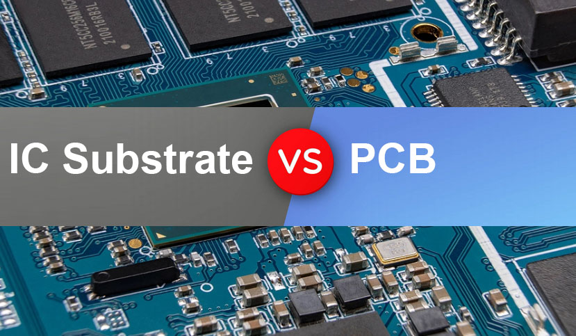
IC substrate vs PCB
The differences between IC substrate and PCB are mainly reflected in the definition, materials, structure, manufacturing process and application scenarios. In this article, Jieduobang will introduce the differences between IC substrate and PCB in detail.
Definition
PCB is the support of electronic components and the carrier for the electrical connection of electronic components; IC substrate is an integrated circuit chip carrier used to install integrated circuit chips and provide electrical connections with extremely high density and reliability.
Materials
PCB uses conductive and insulating materials such as copper clad laminate, glass fiber material and PTFE material; IC substrate mainly uses polymer materials (such as FR-4) and brittle ceramic materials.
Structure
PCB is composed of circuit boards by stacking multiple board layers, which can be connected through holes; the structure of IC substrate mainly includes circuit layer and assembly layer.
Manufacturing process
PCB manufacturing includes steps such as design, graphic layout, patch, welding and testing; IC substrate needs to undergo tedious processes such as preheating, pitting and buttoning.
Application of IC substrates
PCBs are widely used in the field of electronic product manufacturing, such as computer motherboards, mobile phone circuit boards, etc.; IC substrates are small, high-density, and highly reliable, and are widely used in high-end electronic fields, such as aerospace, national defense, and automotive electronics.
The standard thickness of a PCB is often 1.6 mm. This has become the go-to thickness in the industry because it balances flexibility, cost, and performance for most applications. However, depending on the requirements of the design, PCB thickness can vary widely.
Manufacturers offer various thicknesses to accommodate specific designs, from 0.4 mm (0.016 inches) for ultra-thin, flexible boards, up to 3.2 mm or even thicker for high-current, rugged applications. The choice of thickness largely depends on the type of application and the mechanical strength needed.
How is PCB Thickness Measured?
Measuring PCB thickness accurately is crucial for ensuring the board meets design specifications and performs optimally in its application. The thickness of a PCB refers to the total height of the board, including all its layers—copper, dielectric, and solder mask. This thickness plays a role in many factors, from electrical performance to mechanical stability, and must be precisely controlled. The tools and methods used to measure PCB thickness include:
1. Micrometers
A micrometer is the most common tool for measuring PCB thickness. It allows precise measurements down to fractions of a millimeter, making it ideal for multilayer PCBs where small deviations can affect performance. The micrometer is placed at various points across the board to ensure uniform thickness.
2. Calipers
Digital or analog calipers are also used to measure the thickness of PCBs. They are particularly useful for quickly gauging thickness across different sections of the board.
3. Cross-Sectioning
In cases where even more precision is required, manufacturers may opt to cross-section the board. This involves cutting a sample of the PCB and measuring it under a microscope to analyze each layer’s contribution to the overall thickness.
PCB thickness is typically measured in mils (1 mil = 0.001 inches) or millimeters, depending on the region and industry. Standard PCB thicknesses usually fall between 0.4 mm (0.016 inches) and 3.2 mm (0.125 inches), but custom designs may require other dimensions.
In mass production, quality control procedures are in place to ensure that the boards maintain a consistent thickness across large batches. Thickness tolerances range from ±10% to ±20%, depending on the manufacturer and materials used.
How Thick is a 2-Layer PCB Board?
A standard 2-layer PCB is typically 1.6 mm thick, but this can vary based on specific requirements. The board consists of two copper layers, one on each side of the insulating core.
Core Thickness: The thickness of the insulating material between the two copper layers is generally around 1.4 mm.
Copper Thickness: Standard copper thickness is 35 μm (1 oz copper), though this can be adjusted for higher current-carrying capacity.
For lighter applications, such as compact consumer electronics, a thinner board of 0.8 mm may be used, providing more flexibility and space-saving. Meanwhile, more robust applications may demand thicknesses exceeding 2.4 mm.
How Thick is a Standard 8-Layer PCB?
When it comes to multilayer PCBs like the 8-layer variant, thicknesses usually range from 1.4 mm to 2.4 mm, depending on the design requirements. With multiple layers of copper and insulating material stacked together, manufacturers must optimize thickness while considering electrical performance and mechanical rigidity.
Each additional layer introduces more copper and insulation, increasing the overall thickness. For high-frequency applications or boards that must handle significant current, thicker boards may be necessary to ensure signal integrity and thermal management.
How Does PCB Thickness Affect Thermal Performance?
The influence of PCB thickness on thermal performance is mainly reflected in heat dissipation efficiency and heat capacity.
The thickness of the PCB directly affects its heat dissipation efficiency. Thicker PCBs have greater heat capacity and better heat conductivity, and are able to conduct the heat generated by electronic components more effectively. This is because copper has good thermal conductivity, and the thicker copper foil layer can more quickly transfer heat from the heating element to the cooling area or external radiator, helping to improve the overall thermal management efficiency and protect sensitive components from thermal damage.
In addition, the thickness of the PCB is also closely related to its mechanical strength and stiffness. Thicker PCB boards have higher flexural stiffness and impact toughness, can withstand greater mechanical stress and vibration, and ensure the stability and reliability of electronic equipment in harsh environments. This is equally important in thermal management, as it helps to maintain the stable operation of electronic equipment in high temperature environments and prevent performance degradation or damage due to overheating.
However, it is important to note that while thicker PCBs are good for heat dissipation, in high-frequency applications, excessively thick PCBs may increase the impedance and coupling of the signal, thus affecting electrical performance.
What Factors Influence PCB Thickness?
PCB board thickness is one of the key parameters to be considered in the design process, which has a great impact on the performance and reliability of the circuit board. When choosing plate thickness, the following factors need to be considered:
1. Signal speed
The thinner the plate, the faster the signal speed, and vice versa. However, when the board thickness is less than 0.8mm, the signal will have a great loss, will produce serious signal interference, affecting the normal work of the circuit board.
2. Heat conduction
The thinner the board thickness, the worse the heat dissipation ability, easy to produce hot spots and thermal runaway phenomenon, affecting the performance and reliability of the circuit board.
3. Mechanical strength
The greater the thickness of the plate, the higher the mechanical strength, the smoother the surface of the plate, and the greater the bending strength. However, too thick a board will affect the assembly and size of the board design.
4. Number of layers
More layers mean a thicker board. A single-layer PCB may be as thin as 0.4 mm, while multilayer boards like an 8-layer PCB may reach over 2 mm.
Taking the above factors into consideration, it is usually appropriate to choose the plate thickness between 1.6mm-2.0mm.
How to Decide PCB Thickness?
According to different applications and needs, PCB board can be divided into a variety of thicknesses, commonly used board thickness is 0.8mm, 1.0mm, 1.2mm, 1.6mm, 2.0mm and so on. When selecting PCB board thickness, it is necessary to make comprehensive consideration according to specific application scenarios and design requirements. Here are a few ways to choose plate thickness:
1. Determine according to the circuit complexity and working environment
When the circuit complexity is high, multiple components need to be connected at the same time, or the circuit board needs to work in a high temperature environment, you are advised to select a thicker board thickness to effectively improve the performance and reliability of the circuit board.
2. Determine the device size and type
If the device size is small and requires precision assembly, a thinner plate thickness is recommended. For large devices, such as power switches and high-power LED lights, it is recommended to choose a thicker board thickness.
3. Determined according to design requirements and cost control
In terms of cost control, the thinner the plate thickness, the higher the corresponding plate cost will be. Therefore, the cost and performance should be considered comprehensively in the design, and the most appropriate plate thickness should be selected.
The board thickness below 1.0mm is generally used for small electronic devices and mobile devices, such as smart watches, Bluetooth headsets and so on.
1.0mm-1.6mm PCB thickness is suitable for most common electronic devices, such as smart phones, tablets, digital cameras, etc.
Thickness >1.6mm is generally used for industrial control equipment, power switches and other large electronic equipment.
At EBest Circuit (Best Technology), we specialize in manufacturing high-quality PCBs tailored to meet your exact design specifications. We offer custom thickness options for single-layer, double-layer, and multilayer boards.
We understand that PCB thickness is critical to performance, whether you’re working on high-current applications or compact designs. Our team of experts can guide you through the selection process, ensuring that your boards are not only optimized for electrical performance but also for thermal and mechanical stability.
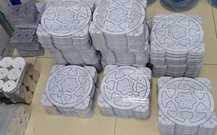
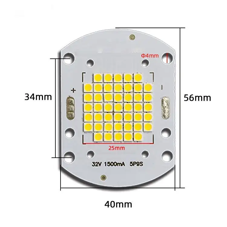
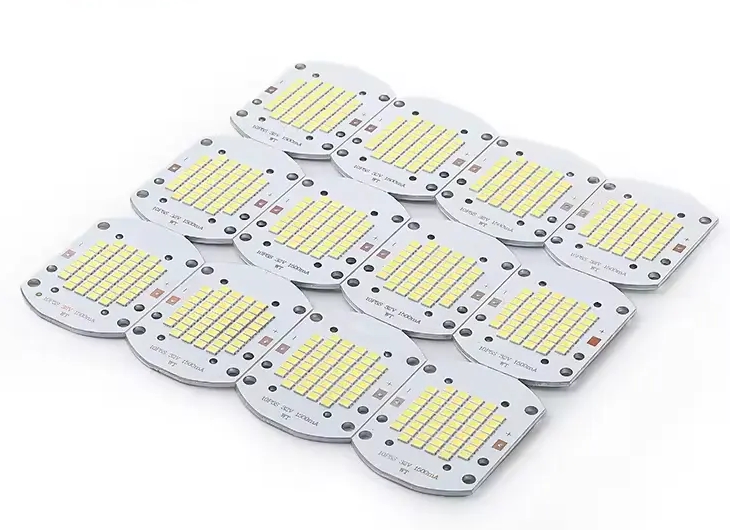
Being the market leader, we offer high quality range of LED Street Light MCPCB or Street Light PCB. These PCB are manufactured using high grade raw material under the supervision of expert and professional team with international quality standards.
These Street Light PCB are available for our valuable customers at affordable cost in market. Due to their precise design and high functionality our offered materials are ideal for making wide variety of led street light of various watt and models.
Street Light MCPCB
MCPCB production process
Substrate preparation: Select appropriate metal substrates, such as aluminum, iron, copper, indium copper, tungsten-molybdenum alloy, etc., as the base of MCPCB. These metal substrates have good thermal conductivity and are the core components of MCPCB.
Insulating dielectric layer coverage: Cover the metal substrate with an insulating dielectric layer. Common insulating dielectrics include modified epoxy resin, polyphenylene ether, polyimide, etc. This layer not only provides the insulation performance required by the circuit, but also enhances the mechanical strength and durability of the MCPCB.
Copper layer laying: Lay the copper layer on the insulating dielectric layer to form the conductive part of the circuit. The copper layer is made through the production process of printed circuit boards, and the corresponding circuits are laid according to the needs of electronic circuits.
Thermocompression bonding process: The metal substrate, insulating dielectric layer and copper layer are combined together through the thermocompression bonding process to form the basic structure of the MCPCB. This step ensures the close bonding between the layers and improves the stability and reliability of the MCPCB.
Circuit production: According to the design requirements, circuit lines are made on the copper layer. This includes drilling, dry film covering, exposure, development and other steps to ensure the accuracy and conductivity of the circuit line.
Inspection and testing: Inspect and test the completed MCPCB to ensure that its performance meets the design requirements. This includes inspection of the circuit surface and aluminum base surface, as well as testing of conductivity and insulation performance.
What are the advantages of mcpcb
Excellent heat dissipation performance: MCPCB usually adopts aluminum substrate or copper substrate, which has good thermal conductivity, can effectively dissipate the heat generated by electronic components, and improve the stability and reliability of the circuit board. This excellent heat dissipation performance makes MCPCB particularly suitable for high switching power applications, such as LED lighting, power modules, automotive electronics and power electronics, among which LED lighting is one of the most widely used fields of MCPCB.
High mechanical strength: The base material of metal core PCB is thicker, with high mechanical strength and bending and torsion resistance, which is conducive to the assembly and transportation of electronic products. This feature makes MCPCB perform well in environments that need to withstand greater physical pressure or frequent movement.
Reliable welding performance: After the surface of metal core PCB is coated with solder paste, it has good welding performance and is suitable for surface mount technology (SMT) and plug-in welding technology. This feature improves the applicability of MCPCB in PCBA processing, making it a preferred material in the manufacture of modern electronic products.
Corrosion and wear resistance: Metal core PCB has strong corrosion resistance and wear resistance, which is suitable for electronic products in harsh environments. This feature enables MCPCB to work stably for a long time under high temperature, humidity or other extreme conditions, improving the durability and reliability of the product.
Space saving: Compared with traditional FR-4 substrates, MCPCB has higher heat dissipation performance, which can design smaller electronic products and save space. This advantage is particularly important in devices with limited space, such as portable electronic devices such as smartphones and tablets.
Improve reliability: Good welding performance and corrosion resistance can improve the reliability and stability of the circuit board and reduce the failure rate. This is especially important in critical systems and equipment, such as medical equipment, industrial control systems, etc., where reliability and stability are crucial factors.
What accessories does a street lamp have?
Lamp holder. The lamp holder of a street lamp is usually an LED lamp, which is the core part of the street lamp. It is responsible for converting electrical energy into light energy to provide lighting services for people. The quality of the lamp holder directly affects the lighting effect and life of the street lamp.
Lamp pole. The lamp pole is the part that supports the lamp holder. It is usually made of metal and has various shapes such as conical poles and prismatic poles. Street lamps in different scenes may require lamp poles of different heights and shapes to meet lighting needs. In addition, safety issues should also be considered, such as anti-theft design and prevention of excessive wind force. In addition, installation accessories such as clamps are also used to fix the lamp pole.
Light source. The light source is an important part of the street lamp, including LED lamp beads, bulbs, etc. The choice of light source is related to key indicators such as brightness, energy consumption and life of the street lamp. At present, LED light sources are widely used in street lamps due to their high efficiency, energy saving and long life.
Electrical control device. The electrical control device includes components such as ballast, trigger, light control switch, etc., which are used to control the working state of the street lamp and protect the circuit safety. For example, light-operated switches can automatically turn streetlights on and off according to ambient light, saving energy. In addition, some advanced streetlights may also be equipped with intelligent control systems to achieve remote monitoring and management.
Installation accessories. These include small parts such as clamps and screws. Although these parts are not conspicuous, they are very important for the installation and maintenance of streetlights. For example, clamps are used to fix the connection between the top of the lamp pole and the lamp head, and screws are used to fix various parts to ensure the stability and safety of the streetlight.
What are the street lights?
Ordinary street lights Ordinary street lights are the most common lighting facilities on the streets. They usually use light bulbs or LED lamp heads and are installed on light poles to provide basic lighting for pedestrians at night.
Solar street lights Solar street lights are an environmentally friendly street light that uses solar panels to absorb solar energy, converts energy into electrical energy, stores it in batteries, and lights up the street lights at night through control devices. Solar street lights do not need to be connected to an external power supply, have low maintenance costs, and are widely used in parks, suburban roads and other places.
LED street lights LED street lights use light-emitting diodes as light sources, which have the advantages of high efficiency, energy saving, long life, safety and reliability. LED street lights have good lighting effects and can be intelligently adjusted according to different environments. They are the first choice for modern urban street light renovation.
Landscape street lights In addition to the basic lighting function, landscape street lights also emphasize artistic decorative effects. It is usually integrated with the surrounding environment, with unique design and diverse shapes, and is used to increase the beauty and cultural atmosphere of street landscapes.
Multifunctional street lights Multifunctional street lights integrate multiple functions such as lighting, monitoring, and communication. In addition to providing lighting, this type of street lamp is also equipped with cameras, display screens and other devices for urban management and security monitoring.
Electricity is ubiquitous in our lives, and the use of all devices is closely related to electricity. The use of electricity depends on how to control and convert it. Among them, the indispensable tools are inverters and converters, which can convert electrical energy into different forms to meet various needs.
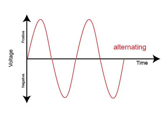
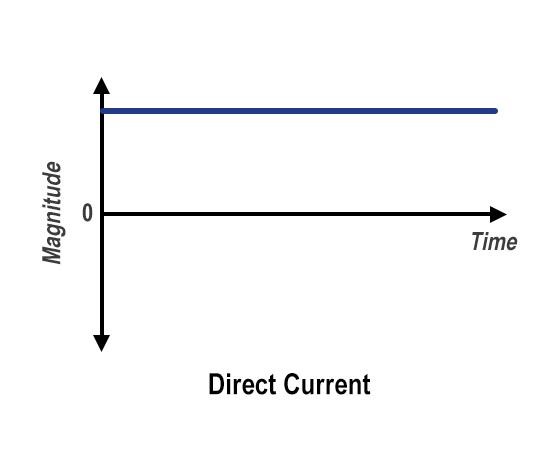
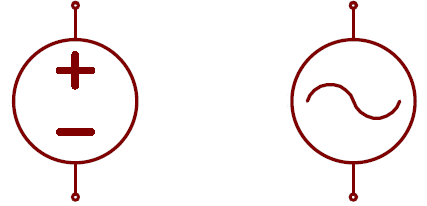
What are AC and DC?
1. Definition of alternating current and direct current:
Alternating current (AC) refers to the current whose direction changes periodically over time, and the average current in one cycle is zero.
The waveform of alternating current is usually a sine curve, but there can also be other waveforms, such as triangular waves and square waves. Alternating current is widely used in power transmission and industrial applications.
Direct current (DC) refers to the current whose direction is constant.
The magnitude and direction of direct current do not change with time. Common DC power sources include dry batteries and storage batteries. The direction of pulsating direct current does not change, but the magnitude changes with time. It usually needs to be filtered to become smooth direct current.
2. The difference between AC and DC:
The main difference between AC and DC is whether the direction of the current changes over time.
The direction of AC changes periodically, while the direction of DC remains unchanged. In addition, the average value of AC in a cycle is zero, while the current and voltage of DC remain constant.
3. Application scenarios of AC and DC:
AC is mainly used for power transmission and industrial applications because its waveform is a sinusoidal curve, which is suitable for long-distance transmission. DC is often used in situations where constant current is required, such as battery-powered electronic devices.
How do you convert from DC to AC?
DC can be converted into AC through an inverter. The inverter usually consists of an inverter bridge, control logic, and filter circuits.
Inversion is a current conversion process opposite to rectification, which converts DC into AC. When the inverter side, i.e., the AC side, is connected to the power grid, it is called active inversion, and when the inverter side, i.e., the AC side, is directly connected to the load, it is called passive inversion.
The inverter circuit can convert DC power into AC power of any frequency and voltage under the control of the control circuit, so it is widely used, for example, when DC power is needed to supply power to AC loads.
What is dc to ac inverter?
Inverter is a device that converts DC power into AC power.
The inverter is mainly composed of an inverter bridge, control logic and filter circuit, which can convert DC power (such as batteries, storage batteries) into fixed frequency and voltage or frequency and voltage AC power, usually 220V, 50Hz sine wave.
Inverters are particularly widely used in automobiles. They can drive various electrical appliances and tools by connecting to batteries, making it possible to use household appliances when driving or traveling.
Inverters can be divided into sine wave inverters and square wave inverters according to the output waveform. Although the sine wave inverter is more expensive, it can be applied to various loads, and the output waveform is closer to the mains, which is friendly to electrical equipment.
The efficiency of the inverter is an important indicator of its performance, which indicates the ratio of output power to input power. With the development of technology, inverters are showing a trend of high frequency, high performance and miniaturization, and are widely used in various fields of power electronics technology.
What is dc to ac converter?
An AC to DC converter is a device whose main function is to convert alternating current (AC) into direct current (DC). Such converters are commonly used in household appliances, computers, mobile phone chargers and other devices to convert the AC power provided by the power grid into the DC power required by the device.
The working principle of the AC/DC converter involves converting the AC power into smooth DC power through a rectification and filtering process. This converter can be bidirectional in terms of power flow, that is, power can flow from the power source to the load (called rectification) or from the load back to the power source (called active inversion).
The working principle of the AC/DC converter involves several key steps:
Rectification: Converting AC power into unidirectional pulsating DC power is achieved by using a rectifier, which can be a half-wave rectifier or a full-wave rectifier, depending on the specific technology used.
Filtering: Filtering is performed by using capacitors to eliminate the pulsating components generated during the rectification process to obtain a smoother DC power.
Voltage stabilization: In some applications, voltage stabilization may also be required to ensure the stability of the output voltage.
The design and application of AC/DC converters are limited by many factors, including safety standards, electromagnetic compatibility (EMC) requirements, and power system optimization design.
In addition, the use of high-voltage, high-current switches increases the power consumption, which to a certain extent limits the modularization process of AC/DC converters.
What is the difference between an inverter and converter?
The main difference between an inverter and a converter is that they have different functions and conversion directions.
Although inverters and converters sound similar, their functions and conversion directions are completely different. The main function of an inverter is to convert direct current (DC) into alternating current (AC), while a converter does the opposite, converting AC into DC. This difference makes them play their respective roles in different application scenarios.
1. Inverter:
The main application of an inverter includes converting electricity generated by a DC power source (such as a battery) into AC to meet the needs of AC equipment. The advantages of the inverter include high conversion efficiency, fast startup, good safety performance, etc., but it may also generate noise due to its working principle, and corresponding countermeasures need to be taken to reduce the noise.
2. Converter:
Unlike the inverter, the main function of the converter is to convert AC to DC.
This is usually achieved through the process of half-wave rectification and full-wave rectification, which involves passing the positive half-cycle or positive and negative cycles of AC through the rectifier circuit, and then further processing through capacitor filtering and voltage stabilization circuit to finally obtain DC.
Converters are widely used in various electronic devices that need to convert AC power to DC power.
In general, although inverters and converters are similar in name, their functions and conversion directions are completely different. Inverters convert DC to AC and are suitable for using DC power for AC devices; while converters convert AC to DC to meet the needs of devices that require DC power.
Why would you use an inverter?
The main reason for using an inverter is to convert DC to AC to meet the power needs of various devices and systems.
The main function of the inverter is to convert direct current (DC) into alternating current (AC), which is necessary in many fields and scenarios. Here are some of the main uses of the inverter:
1. Household electricity: The inverter can convert the DC power of the car battery or other DC power source into the AC power required by household appliances, so that the car or other DC power source can power household devices.
2. Emergency power supply: In the event of a power outage or power outage, the inverter can convert the DC power of the backup power source (such as gasoline generators, solar panels, etc.) into AC power to provide power support for key equipment.
3. Electronic devices: Many portable electronic devices (such as laptops, mobile phones, cameras, etc.) use DC batteries as power sources. The inverter can convert DC power into AC power to provide power for these devices.
4. Industrial applications: In industrial production, the inverter can convert high-voltage DC power into low-voltage AC power to meet the power needs of different equipment and systems.
5. Electric vehicle charging: With the popularity of electric vehicles, inverters are increasingly used in electric vehicle charging stations, which convert direct current from the power grid into alternating current required by electric vehicle batteries.
6. Radio communication: In radio communication, inverters are used to convert direct current into radio frequency power to transmit and receive radio signals.
Therefore, inverters play an indispensable role in modern society and are widely used in various fields to provide necessary power conversion and support for various devices and systems.
What are the disadvantages of an inverter?
1. Harm to batteries: Inverters increase the burden on batteries and shorten the life of batteries. Inverters generate electromagnetic interference and heat when working, which may interfere with batteries, causing unstable battery voltage or internal damage to batteries.
2. Energy loss: The conversion efficiency of inverters is relatively low, and there will be a certain amount of energy loss.
3. High cost: The cost of inverters is high, which may not be suitable for some low-cost applications.
4. May generate electromagnetic interference and heat: The inverter will generate high-frequency electromagnetic waves and a certain amount of heat when working, which may affect the working performance of other electronic equipment and may even cause safety problems.
In summary, although the inverter provides convenience in many applications, its disadvantages cannot be ignored, including energy loss, high cost, possible electromagnetic interference and heat, and potential safety hazards.
Conclusion:
Inverters and converters are indispensable in modern electrical systems to ensure that energy flows to where it is needed in the right form. Whether it is converting DC to AC for renewable energy systems, using batteries to power equipment, or ensuring uninterruptible power supply, these tools can achieve a smooth transition between different types of current.
1). 99 alumina 99 alumina refers to alumina materials with a purity of 99% or higher. It is usually made of chemically pure alumina or high-purity alumina as raw materials, and is made through multiple processes such as high-temperature calcination, crushing, molding, and sintering. Compared with 96 alumina, 99 alumina has higher chemical purity, density and hardness, as well as better high-temperature stability and corrosion resistance.
99 alumina is widely used in electronics, machinery, chemical industry, aerospace and other fields. In the electronics field, 99 alumina is usually used to manufacture high-frequency electronic components, integrated circuit packaging, dielectrics and other devices; in the mechanical field, 99 alumina is mainly used to manufacture high-hardness ceramic tools, bearing balls, etc.; in the chemical field, 99 alumina can be used to manufacture catalysts and adsorbents; in the aerospace field, 99 alumina is often used to manufacture high-temperature structural parts, aircraft engine parts, etc.
2). 96 alumina 96 alumina, also known as industrial alumina or α-alumina, is a high-purity ceramic material. Its chemical formula is Al2O3, which belongs to oxide ceramics. 96 alumina is usually made of alumina powder through pressing, molding, sintering and other processes. The “96” here means that its aluminum oxide purity reaches more than 96%. 96 alumina has the characteristics of high hardness, high strength, high wear resistance, and good high temperature stability. It is widely used in the manufacture of ceramic products, refractory materials, abrasives, electronic devices and other fields.
Advantages of 99 alumina substrate:
High purity, usually reaching a purity level of 99.99%, excellent electrical properties, high dielectric constant and low dielectric loss. Good high temperature stability, can work stably in high temperature environment, and can usually withstand temperatures up to 1700℃. High mechanical strength, high strength, high hardness, not easy to be damaged, and can withstand greater force and pressure. It has excellent corrosion resistance, is not corroded by most chemical substances, and is suitable for chemical media such as acids and alkalis. It can be prepared into a thinner substrate, which is conducive to the preparation of microelectronic devices.
Advantages of 96 alumina substrate: Cheaper than 99 alumina substrate, the cost is relatively low. It is easier to process than 99 alumina substrate, and can be processed by cutting, drilling and other processing, which is convenient for preparing substrates of various shapes. In some low-temperature and low-electric field strength applications, the dielectric constant and dielectric loss are lower than those of 99 alumina substrate, and it has better signal transmission performance.
Disadvantages: Compared with 99 alumina substrate, 96 alumina substrate has lower purity, higher dielectric constant and dielectric loss. It is prone to brittle fracture in high temperature environment.
Alumina ceramic application industry 99 alumina substrate: suitable for high-power LED, high-voltage integrated circuit, high-temperature sensor, high-frequency electronic components and other fields. 96 alumina substrate: suitable for low-power electronic components, sensors, capacitors, micro relays, microwave components and other fields.
Aluminum nitride ceramic is a high-performance ceramic material made of aluminum nitride powder sintered at high temperature. Its main component is aluminum nitride (AlN), which has the characteristics of high melting point (about 2800℃), hardness (9.0 to 9.5Mohs), strength and thermal conductivity. At the same time, it also has good insulation performance, chemical stability and high temperature resistance. Due to these characteristics, Sliton aluminum nitride ceramic circuit boards are widely used in microelectronics, optoelectronics, power electronics, aerospace and other fields.
Advantages
High hardness: The hardness of aluminum nitride is close to that of diamond, which is more than 3 times that of traditional alumina. It can be used to make high-strength mechanical parts.
High strength: Aluminum nitride has high strength, good wear resistance and corrosion resistance, and can be used to make high-load, high-wear and corrosion-resistant parts.
High thermal conductivity: The thermal conductivity of aluminum nitride is very high, reaching 170-230W/(m·K), which is more than 4 times that of traditional aluminum oxide. It can be used to make high-power, high-frequency RF components.
High insulation: The dielectric constant of aluminum nitride is low, about 1/3 of that of traditional aluminum oxide, and can be used to make high-frequency, high-precision microwave components.
Anti-oxidation: Aluminum nitride has good anti-oxidation properties at high temperatures and can be used to make parts in high-temperature environments.
Application of aluminum nitride ceramics Widely used in semiconductors, aerospace, electronics, military and other fields. For example, it is used to make high-frequency RF devices, microwave components, electronic ceramics, thermistors, high-temperature sensors, etc.
Zirconium oxide ceramic material is a ceramic material with high strength, high hardness, high temperature tolerance, corrosion resistance and good insulation performance. Its chemical formula is ZrO2, and it is usually stabilized to improve the stability and wear resistance of its lattice. Zirconia ceramic material has the characteristics of low thermal conductivity and high melting point, so it is widely used in industrial fields with strict requirements such as high temperature, high pressure, high speed and high precision, such as aerospace, electronics, medical and energy. Advantages
High hardness: The hardness of zirconia ceramics is very high, usually reaching HRA90 or above, even up to HRA95, which is more than 10 times that of steel.
High strength: Zirconia ceramics have extremely high strength, which can reach 900MPa at room temperature, and can still maintain high strength at high temperature.
Good wear resistance: Zirconia ceramics have high surface flatness and high hardness, so they have good wear resistance.
Good corrosion resistance: Zirconia ceramics are chemically inert and not easily corroded by chemicals such as acids and alkalis, and can operate stably for a long time in harsh environments.
Excellent insulation performance: Zirconia ceramics have excellent insulation performance and can be used for high-voltage insulation materials.
Good high-temperature stability: Zirconia ceramics have extremely high melting points and high-temperature stability, and can be used for a long time in high-temperature environments.
Application of Zirconia Ceramics Widely used in high-end manufacturing, electronics, aerospace, medical equipment, chemical industry and other fields, such as abrasives, high-temperature structures, pneumatic components, medical equipment, sensors, capacitors, etc.
Silicon carbide is a compound with the chemical formula SiC, which is composed of two elements: silicon and carbon. It is a ceramic material that is resistant to high temperature, corrosion, and extremely hard. It is also an industrial material widely used in extreme environments such as high temperature, high frequency, and high pressure. Silicon carbide has excellent mechanical, electromagnetic, and thermal properties, and is therefore widely used in semiconductors, disks, aerospace, and other fields. In addition, silicon carbide has good semiconductor properties and is also widely used in power electronics, optoelectronics, and other fields. Advantages
High hardness: The hardness of silicon carbide material is 5 times higher than that of steel and 3 times higher than that of aluminum.
High strength: The strength of silicon carbide material is high, and the tensile strength can reach more than 400MPa.
High temperature resistance: Silicon carbide material has a high melting point and can withstand high temperature thermal shock. The general use temperature is 1200℃-1600℃.
Good oxidation resistance: Silicon carbide material can resist high temperature oxidation corrosion and can be used in air.
Good wear resistance: Silicon carbide material has high hardness, low friction coefficient and good wear resistance.
Good thermal conductivity: Silicon carbide material has excellent thermal conductivity, which is 2-3 times that of metal and can effectively dissipate heat.
Good chemical stability: Silicon carbide material has good chemical stability and will not be corroded by acid, alkali, etc.
Silicon carbide ceramic PCB application Widely used in high temperature, high pressure, high speed, high load, corrosion resistance and other fields, such as power, electronics, machinery, aviation, metallurgy and other industries.
Silicon nitride ceramic material (Si3N4)
Silicon nitride ceramic material is a high-temperature ceramic material based on nitrogen and silicon elements. It has excellent properties such as high strength, high hardness, high wear resistance, high temperature resistance, oxidation resistance, and corrosion resistance. Its chemical stability is extremely high and is not easily corroded by acids, alkalis, solvents, etc. The hardness of silicon nitride ceramic materials is comparable to that of diamond, or even higher, reaching about 24GPa. It is harder and less prone to wear than ordinary ceramic materials. At the same time, it has good insulation properties and thermal stability, and can work stably for a long time in high temperature environments.
High hardness: The hardness of silicon nitride ceramic materials is close to that of diamond, which can reach more than 30GPa.
High strength: The bending strength of silicon nitride ceramic materials is high, which can reach more than 1000MPa.
High wear resistance: Silicon nitride ceramic materials have good wear resistance and can be used to manufacture high-speed bearings and cutting tools, etc.
High temperature resistance: Silicon nitride ceramic materials have high high temperature resistance and can be used in high temperature environments above 1000°C.
Corrosion resistance: Silicon nitride ceramic materials have excellent corrosion resistance and can be used in some acidic and alkaline working environments.
Lightweight: Silicon nitride ceramic materials are lighter than steel and can be used in lightweight design.
Silicon nitride ceramic PCB applications Widely used in aerospace, optoelectronics, electronics, semiconductors, machinery and other fields.
Piezoelectric ceramic materials
Piezoelectric ceramic materials are ceramic materials with piezoelectric effect, which can deform under external electric field or mechanical stress, and generate electric charge when deformed. They are usually made of materials such as barium lead oxide (Pb(Zr,Ti)O3) or niobium lead oxide (Pb(Mg1/3Nb2/3)O3-PbTiO3) as the main components and sintered.
Advantages
Piezoelectric effect: It can convert mechanical stress into electrical signals, or convert electrical signals into mechanical motion. This effect makes piezoelectric ceramic materials widely used in sensors, actuators, acoustic wave devices and other fields.
Dielectric properties: With high dielectric constant and low dielectric loss, piezoelectric ceramic materials are used as capacitors, filters, etc. in electronic components.
Mechanical properties: With high hardness, strength and wear resistance, piezoelectric ceramic materials are used in mechanical engineering.
Thermal stability: With good thermal stability and high temperature resistance, it can work stably in high temperature environment. Piezoelectric ceramic PCB applications Widely used in sensors, actuators, acoustic wave devices, electronic components, mechanical engineering and other fields.
Diamond ceramic material
Diamond ceramic material is a new type of material made by sintering diamond powder and ceramic as raw materials at high temperature and high pressure. Because diamond has extremely high hardness, reaching Mohs hardness level 10, and has excellent wear resistance, corrosion resistance and high temperature oxidation resistance, diamond ceramic material has extremely high physical and chemical properties.
Extremely high hardness and strength, more wear-resistant, scratch-resistant and impact-resistant than ordinary ceramic materials;
Excellent corrosion resistance, able to resist corrosive media such as strong acids and alkalis;
Excellent high-temperature oxidation resistance, can be used for a long time at high temperature without damage;
Excellent thermal conductivity and insulation performance;
Easy to process into ceramic products of various shapes and sizes.
Application of diamond ceramic PCB Diamond ceramic materials are widely used in high-end machinery, electronics, optics, medical and chemical fields, such as bearings, nozzles, cutting tools, hydraulic cylinders, electrical insulation parts, laser parts, etc.
Sapphire ceramic material
Sapphire ceramic material, also known as synthetic sapphire (Synthetic Sapphire), is a man-made single crystal material with excellent properties such as high hardness, high wear resistance and high corrosion resistance. The main component of sapphire ceramic material is aluminum oxide (Al2O3), which is prepared by melting or heat treatment at high temperature.
Advantages of sapphire ceramic material:
High hardness: The hardness of sapphire ceramic material is second only to diamond, and it has high wear resistance.
High corrosion resistance: Sapphire ceramic material has excellent corrosion resistance and can be used stably for a long time in harsh environments such as strong acid and strong alkali.
High light transmittance: Sapphire ceramic material has high light transmittance and can be used in optics, laser and other fields.
Even though we live in a world full of electronic gadgets, electronic devices are still shrouded in mystery. The working principle of electronic projects may seem very abstract, as the interior of these gadgets does not seem to have any visible mechanical parts. There are no moving parts such as gears or shafts on the printed circuit board, nor any significant visual changes.
The flow of electricity is invisible and can only be perceived by the effect it produces. Therefore, for those who want to dabble in the field of electronics making, making electronics as a hobby can seem like an extremely challenging task. It seems hard to imagine building something without fully understanding the principles behind it.
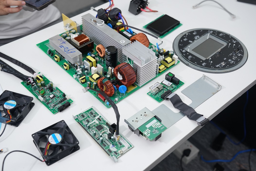
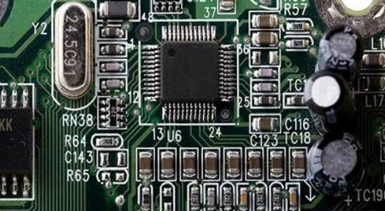
What does PCBA mean?
PCBA is the abbreviation of Printed Circuit Board Assembly, which refers to the process of welding, inserting, etc. of electronic components to the circuit board, and welding, inserting, etc. PCBA is an indispensable and important link in the manufacture of electronic products, which directly affects the performance stability and service life of electronic products.
The manufacturing process of PCBA mainly includes components mounting, welding, post-welding processing and functional testing. The first is the component mounting, which is a process of welding the patch components, plug-in components, etc., to the PCB. Then there is welding, through traditional wave soldering or modern lead-free welding and other methods, the components are firmly fixed on the PCB. After that, the welding process is mainly to remove the welding slag on the PCBA surface, clean the PCBA surface, and check the solder joints and components of PCBA. Finally, the functional test is carried out, which is the last step in the PCBA process, and the PCBA is fully functional tested by various test equipment to ensure the stability and reliability of PCBA.
Applications of PCBA
PCBA products are widely used in various electronic products, such as household appliances, communication equipment, automotive electronics, industrial control equipment, etc. You can see it everywhere.
Different electronic products have different requirements for PCBA. Some require PCBA to be small and exquisite, some require PCBA to be high temperature and high pressure resistant, and some require PCBA to be waterproof and dustproof. With the rapid development of 5G, artificial intelligence, Internet of Things and other fields, PCBA will be more widely used, and PCBA’s performance and reliability requirements will also be higher.
Common components on a PCBA and their symbols
1. Resistor
Resistors are one of the most commonly used electronic components in PCBA, used to limit the current in the circuit. According to different materials, structures, and resistance values, resistors can be divided into fixed resistors, variable resistors, and special resistors. Resistors are widely used in various circuits, such as power circuits, amplification circuits, signal processing circuits, etc., to achieve current regulation and control.
2. Capacitor
A capacitor is a component that stores charge and electrical energy, with the characteristic of blocking direct current and passing alternating current. In PCBA, capacitors are commonly used in circuits such as filtering, coupling, tuning, and bypassing to improve circuit performance and stability. According to their different structures and applications, capacitors can be divided into fixed capacitors, variable capacitors, and fine tuned capacitors.
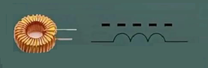
3. Inductor
Inductor, also known as induction coil, has the function of storing magnetic energy. In circuits, inductors can prevent changes in current and play a role in filtering and stabilizing the current. Inductance has a wide range of applications in power filtering, signal processing, and other fields.
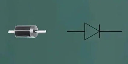
4. Diode
A diode is an electronic component with unidirectional conductivity, widely used in circuits such as rectification, detection, and voltage regulation. In PCBA, diodes can achieve functions such as voltage regulation, signal amplification, and switch control in the circuit. Common diodes include silicon diodes and germanium diodes, whose performance parameters such as forward voltage drop and reverse breakdown voltage determine their application scenarios.
5. Transistor
Transistors are electronic components with functions such as amplification and switching, and are the core components that make up various circuits. In PCBA, transistors are commonly used in amplification circuits, oscillation circuits, switch circuits, etc. to achieve signal amplification, frequency conversion, and circuit control. There are many types of transistors, including bipolar transistors, field-effect transistors, etc., each with its own characteristics, widely used in various electronic devices.
6. IC Integrated circuit
Integrated circuit is an electronic component that integrates multiple electronic components on a single chip, with advantages such as small size, low power consumption, and stable performance. In PCBA, integrated circuits are key components for implementing various complex functions, such as digital signal processing, analog signal processing, communication interfaces, etc. Common integrated circuits include operational amplifiers, logic gate circuits, microprocessors, etc., which are widely used in various intelligent devices and systems.
7. Sensor
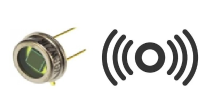
Sensors can sense physical quantities or states in the environment and convert them into electrical signals for output. In PCBA, sensors are commonly used to detect parameters such as temperature, humidity, light, pressure, etc., providing data support for intelligent control of electronic devices. There are various types of sensors with different performances, and choosing the appropriate sensor is crucial for improving the performance and user experience of electronic devices.
8. Controllable silicon rectifier (SCR)
Also known as thyristors, silicon controlled rectifiers (SCR) are similar to transistors and diodes – their working principle is essentially the coordinated operation of two transistors. Although SCR also has three pins, they are composed of four layers of silicon material instead of three layers, and are only used as switches, not amplifiers. Unlike single transistors that require continuous current to remain on, SCR only requires one pulse to activate the switch. They are very suitable for converting large amounts of electricity.
9. Crystal oscillator
Crystal oscillators provide clock signals in many circuits that require precise and stable timing. By physically oscillating piezoelectric materials (such as crystals), they generate periodic electronic signals, hence their name. Each crystal oscillator is designed to vibrate at a specific frequency, which is more stable, economical, and smaller in size than other timing methods. That’s why they are commonly used for precise timing in microcontrollers, or more commonly as clock components in quartz watches.
10. Switches and relays
A basic and easily overlooked component, a switch is simply a power button that controls the current in a circuit by switching between open or closed circuits. They vary greatly in appearance, from sliders, rotations, buttons, levers, toggles, key switches, and more. Similarly, a relay is an electromagnetic switch that operates through a solenoid, acting like a temporary magnet when a current flows through it. They act as switches and amplify small currents into larger ones.
Now that you’re familiar with some basic electronic components, why not dive into creating your own electronics project? Instead of starting with a complex project featuring advanced functions, begin with a few simple ones. As with any hobby, you’ll encounter challenges along the way, but these hurdles are not insurmountable. With accessible and affordable beginner electronics tools like Arduino and CAD tools, the maker community welcomes new PCB designs and projects every day.
In addition to PCB manufacturing, EBest Circuit (Best Technology) offers a full turnkey service, including parts procurement and assembly. Whether you’re working on prototypes or scaling up to mass production, Best Team provides a one-stop solution for seamless and hassle-free PCB assembly.
Relays in power systems are important components that play a vital role in controlling circuits. The core of a relay is an electric switch that can automatically or manually open or close a circuit according to the design. Relays are commonly used in a variety of applications, from small electronic devices to large power systems, and they provide a reliable way to control high-power circuits using low-power signals.
What is relay?
Relay refers to a transfer device in a circuit that controls the switch through the electromagnetic principle to achieve the purpose of automatic control. In power systems, relays can control the switch of circuits by detecting changes in parameters such as current and voltage to achieve protection and control of the system.
The basic working principle of a relay is to use the electromagnetic effect to control the on and off of mechanical contacts. When the coil with an iron core is energized, the coil current generates a magnetic field, which attracts the armature to move, thereby opening and closing the contacts.
Why would you need a relay?
The reasons for needing a relay mainly include safety isolation, remote control, timing or delay control, protection equipment, signal conversion, etc.
1. Safety isolation: When a low-voltage device (such as a microcontroller or sensor) is used to control a high-voltage device, the relay can act as an isolation layer to ensure safe operation.
2. Remote control: When a device needs to be controlled at a longer distance or in a longer environment, the relay can transmit and amplify the signal to achieve remote control.
3. Timing or delay control: When a device needs to be started or shut down at a specific time or after a delay, the relay can achieve timing or delay control.
4. Protective device: As a protective device, the relay can prevent the device from being affected by faults such as overload and short circuit.
5. Signal conversion: When one signal needs to be converted to another, the relay can perform signal conversion, such as converting an analog signal to a digital signal, or converting a wireless signal to a wired signal.
In addition, relays have the advantages of high reliability, long life, and low power consumption, which can improve the safety and stability of the equipment. Therefore, relays are indispensable and important components in automated control circuits, remote control, telemetry, communication, automatic control, mechatronics and power electronic equipment.
What is the main function of a relay?
The main functions of relays include amplifying signals, realizing remote control, protecting circuits, realizing logical control and improving system reliability and stability.
Amplifying signals: Relays can convert weak control signals into stronger control signals. Because the contact capacity of relays is large, they can control loads with large currents and high voltages.
Remote control: Through input signals, relays can control the switch state of load equipment at a distance and realize the function of remote control.
Protect circuit: Relays have overload protection and short-circuit protection functions. When abnormal conditions occur in the circuit, such as overload, short circuit, etc., the relay can automatically cut off the power supply to prevent the fault from expanding and protect the safety of circuits and equipment.
Realize logical control: Relays can realize complex logical control through multiple sets of normally open and normally closed contacts, and are widely used in automation control systems, industrial control and other fields.
Improve the reliability and stability of the system : Relays have high stability and reliability, which can reduce the failure rate in the system and improve the stability and reliability of the entire system.
In addition, relays also have isolation functions, which can protect the control circuit from the influence of the external environment and prevent electric shock accidents, which is very useful in some occasions with high safety requirements.
What is the difference between a switch and a relay?
Switches and relays have significant differences in function, application, structure and usage scenarios.
1. Function and application
Switches are mainly used to connect and disconnect circuits, while relays are mainly used to control the on and off of circuits to achieve protection and control of circuits.
Switches can be regarded as a basic electrical component used to simply connect or disconnect circuits, while relays control the on and off of large currents by controlling small currents in the circuit to achieve remote control or automatic control.
2. Structure and design
The contacts of switches may be small and are generally used to control small currents. In contrast, the contact switches of relays are larger and can be used to drive larger loads.
Contactors generally have arc extinguishing devices, while relays do not. This shows that relays and switches are different in design and application. Relays are more suitable for use in control circuits, while switches are used in main circuits.
3. Use scenarios
Switches are usually used to directly control the on and off of the main circuit, such as motor start-up, shutdown control, etc. Relays are more used in auxiliary circuits, such as the on and off of the control circuit, or after power is on or off, the on and off of the circuit is controlled by the change of position state, or the output node is given to other circuits.
Although switches and relays both play important roles in electrical systems, they have obvious differences in design, function and purpose. Switches are mainly used for simple circuit on and off operations, while relays are more used for the protection and control of control circuits, controlling the on and off of large currents by small currents, and realizing remote control or automatic control.
What is a relay vs fuse?
Fuses and relays play different roles in automotive circuits and have obvious differences.
Fuse is a non-resettable one-time thermal protection device, mainly used for overload protection. When a circuit fails or is abnormal, the current continues to increase. The increased current may damage some important components in the circuit, burn the circuit, or even cause a fire.
The function of the fuse is to disconnect the power supply of the electrical equipment on the vehicle when a short circuit or overload occurs, so as to protect other electrical appliances and lines.
The relay is an automatic control device. When the input (electricity, magnetism, sound, light, heat) reaches a certain value, the output will change in a jump-like manner. Relays are mainly used for overload protection. They control larger currents with smaller currents, and play the role of automatic adjustment, safety protection, and circuit conversion.
The working principle of the relay is to generate a magnetic field through the electromagnet coil, magnetize the iron core, attract it to the magnetic pole of the electromagnet, and then drive the contacts to close or open, so as to realize the switch control of the circuit.
In short, the function of the fuse is to cut off the current automatically when the current abnormally rises to a certain height and heats up, so as to protect the safe operation of the circuit; while the relay protects the circuit and electrical equipment from the influence of overload, short circuit and other faults by controlling the circuit, and at the same time improves the reliability of the circuit operation.
Conclusion:
As technology continues to evolve, relays become more sophisticated and in a world where the demand for power is increasing and the need for reliable power systems is more important than ever, relays will continue to play a vital role in ensuring our power systems remain safe, efficient, and more.
A circuit diagrams, also known as an electrical diagram, schematic diagram, or electronic schematic diagram, is a graphical representation of a simplified circuit. It is a visual tool for the design, construction, and maintenance of electrical and electronic equipment.
By utilizing images or standard symbols of different components, circuit diagrams can simplify the description of the components of a circuit and their interconnections. This enables electricians and technicians to easily understand the relative positions of components and their relationships in the circuit.
How to learn circuit diagram easily?
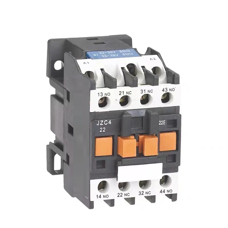
1. Knowing electrical components: First, you need to understand common electrical components, such as AC contactors, push button switches, thermal relays, time relays, etc., and master their working principles and structures.
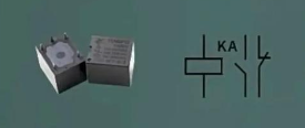
2. Memorizing electrical symbols: Learn and memorize common electrical letters and graphic symbols, such as AC contactors (KM), intermediate relays (KA), etc.
3. Basic theory learning: Have basic electrical basic knowledge, such as the relationship between the rotation direction of a three-phase asynchronous motor and the phase sequence of the power supply.
4. Practical operation: If conditions permit, disassemble electrical components to familiarize yourself with their internal structure, or understand the internal structure and working principle through physical diagrams.
5. Practice step by step: Start with simple circuit diagrams and gradually try to analyze more complex circuit diagrams. Through continuous practice, you can gradually improve your ability to interpret circuit diagrams.
6. Use the principle of circuit simplification: Learn and apply the basic principles of circuit simplification, such as ignoring wire resistance, switch processing, etc.
7. Combine theory with practice: Apply theoretical knowledge to practice, for example, try to design your own circuit based on the learned electrical schematics, or design circuit diagrams according to actual needs.
Through the above steps and methods, you can learn and understand circuit diagrams more easily.
What are the 4 rules for drawing circuit diagrams?
The 4 rules for drawing circuit diagrams are:
1. Circuits or components should be arranged according to function and arranged in working order as much as possible.
2. All electrical components should be represented by graphic symbols and text symbols that are unified by national standards.
3. Different parts of the same electrical component (such as coils and their multiple contacts) are often not drawn together, but should be marked with the same text symbol.
4. In the circuit schematic, all contacts of the control appliance should be drawn in the “non-excitation” state.
These rules together ensure that the circuit diagram is clear, accurate and easy to understand, and provide an important reference for the design and maintenance of electronic equipment and systems.
How to get better at reading schematics?
Understand the basic composition and logic block diagram of the circuit: First, you need to understand the relationship between the various components in the schematic, such as power supply, reset, etc., and the connection relationship between the various devices on the motherboard.
Pay attention to details: When reading the schematic, you need to pay attention to details, such as the model of the components, the connection method, etc.
Do more exercises: Through a lot of reading and practice, you can become familiar with various circuit types and topics and gain more knowledge and experience from them.
Use relevant knowledge of analog circuits and circuit design: Having a deep understanding of the basic concepts and principles of analog circuits and circuit design can help better understand how the various parts in the schematic work together.
What are the components of common circuit schematics?
Power supply: The power supply provides electrical energy to the circuit in the form of voltage and current. Every functional electronic circuit requires a DC or AC power supply.
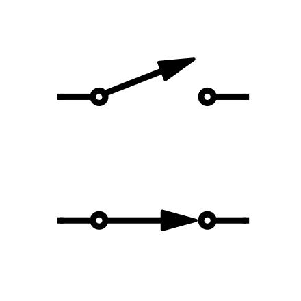
Switches: Switches can make or break connections in a circuit. They can also change the path that current flows.
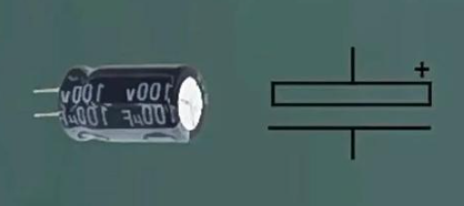
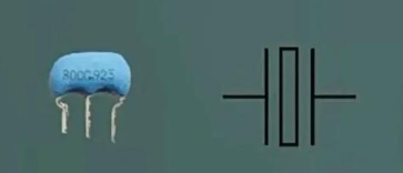
Capacitors: Capacitors are passive electronic components that store electrical charge. There are two common types of capacitors: nonpolar capacitors and polar capacitors.
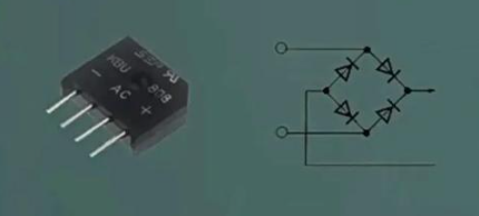
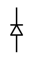
Diodes: A diode is a polarized device that allows current to flow in only one direction. Because it is polarized, it has a positive terminal (anode) and a negative terminal (cathode). The flat side of the triangle is the anode, and the line is the cathode.
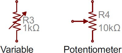
Potentiometers and variable resistors: Both variable resistors and potentiometers have an arrow added to the standard resistor symbol. Variable resistors are still two-terminal devices, so the arrow just goes diagonally through the middle. Potentiometers are three-terminal devices, so the arrow becomes the third terminal (the wiper).
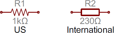
Resistors: The most basic circuit component and symbol, resistors on schematics are usually represented by a few jagged lines with two terminals extending outward. Schematics using international symbols may use a featureless rectangle instead of a wavy line.
What does a resistor do in a circuit?
Resistance (usually represented by “R”) is a physical quantity that indicates the magnitude of the resistance of a conductor to the current in physics.
The greater the resistance of a conductor, the greater the resistance of the conductor to the current. Different conductors generally have different resistances, which is a characteristic of the conductor itself. Moreover, the main functions of resistors in circuits include current shunting, current limiting, voltage division, biasing, filtering (used in combination with capacitors), impedance matching, and converting electrical energy into internal energy.
What is the simplest of all circuit diagrams?
The simplest of all circuit diagrams is the series circuit.
The series circuit is one of the most basic circuit connection methods, consisting of components such as power supply, wires, switches, and electrical appliances. The characteristic of this circuit is that the path of current passing through each component is single, that is, the current flows out from the positive pole of the power supply, passes through each component and reaches the negative pole of the power supply.
The structure of the series circuit is simple and easy to understand and construct. Therefore, the series circuit is an important concept in the basic stage of circuit learning. In addition, the single path nature of the series circuit makes it the basis for understanding and analyzing complex circuits, laying the foundation for subsequent learning of more complex circuit structures such as parallel circuits and hybrid circuits.
Conclusion:
Circuit diagrams are an important tool in the field of electronics that provide a visual representation of circuits. These diagrams are essential for designing, troubleshooting, and understanding how electronic components are interconnected.
Whether you are a beginner or an experienced engineer, mastering the skill of reading circuit diagrams is the foundation for a successful career in electronics. It enables you to effectively design, troubleshoot, and understand electronic circuits. You can master this important skill by becoming familiar with common symbols, understanding circuit layouts, and practicing regularly.
In the field of games, domestic games have always been labeled as “low-quality” and “imitation”, and the emergence of “Black Myth Wukong” has undoubtedly dropped an atomic bomb on the entire game industry, attracting Chinese people to applaud. It will leave a strong mark in the history of games. Since the first trailer was launched, industry peers and players have high expectations for Black Myth, and it has even been dubbed the “light of domestic games”.
What is a 3A masterpiece?
3A masterpieces usually refer to games with high development costs (a lot of money), long development cycles (a lot of time), and high resource consumption (a lot of resources). These games generally have high quality, large development teams, high development budgets, high visual and auditory effects, perfect combination of art and technology, and outstanding ease of use.
3A games represent the pinnacle of production quality, top technology and huge market influence. They are not only entertainment products, but also the perfect combination of technology, art and business. 3A games not only define the highest standards of the industry, but also become the golden benchmark in the minds of global players.
What are the classic 3A masterpieces?
1. Red Dead Redemption 2
The graphics of Red Dead Redemption 2 have reached a very high level in the past and even now. Its game graphics not only show us a real and shocking Western world, but also bring us a brand new experience.
In terms of image quality, it can be said to be top-level. From modeling to scenes and weapons, it is very realistic, and the detailed textures are also very rich, which makes the light in the entire game environment very beautiful, and it can also give players an immersive feeling.
2. Assassin’s Creed: Revolution
This is a high-quality action-adventure game. Players can experience the real style of Paris in the game, and can also choose different professions to unlock different abilities.
The overall picture effect of the game is very good, and the picture quality is also at a very high level. “Assassin’s Creed: Revolution” not only has a very good 3D visual experience, but also has an extremely powerful open world. This world is full of excitement and thrills, and it is a good game.
3. Call of Duty Series
The image quality of “Call of Duty” is relatively top-notch among 3A masterpieces. This is a high-quality 3D game, and the gameplay is very simple, that is, the player controls a special forces soldier to collect resources and ammunition on the battlefield, and use various types of weapons to defeat the enemy.
In addition, it contains not only single-player campaigns, but also cooperative campaigns, multiplayer cooperative campaigns and other types of campaign gameplay. “Call of Duty” also has a very rich map scene, a variety of terrains, weapons, ammunition and other resources and many other elements to provide players with richer content, more gameplay, etc.!
4. Forza Horizon 5
“Forza Horizon 5” is one of the best racing games you can experience at present. Although it has not changed much compared to the previous game, you can still experience the purest driving pleasure in hundreds of hours of game time.
The Mexico map in the game truly reproduces the beauty of various places, from endless deserts to winding wilderness and other terrains, every link allows you to feel its beauty and diversity. In the game, you will not only feel the excitement of racing, but also the shock from the vehicles and maps.
Why is Black Myth Wukong so popular?
For a long time, the production of 3A games has been basically controlled by game developers in Europe, the United States, Japan and other countries. In the field of domestic games, although many excellent works have been launched, before Black Myth Wukong, no single-player game has reached the international 3A game level, nor has it been so concerned by global media and players before it was launched.
“Chinese people do not have the strength to make 3A game masterpieces” “China does not have the soil for 3A games to grow”… For a long time, these statements are almost a factual description of the domestic game market and a helpless consensus of the majority of game players.
The aura of the Journey to the West theme, the desire for domestic 3A masterpieces, and even the hope for cultural inheritance are all placed on “Black Myth Wukong”. As Black Myth Wukong is about to “break out of the stone”, domestic 3A games will finally be subject to the heavy test of the market and players.
Judging from the current development results, the graphics of Black Myth Wukong have reached a very high level, and the unique classical scenes also make domestic 3A games more Chinese.
Industry insiders said that the reason why 3A games are regarded as the top works in the game industry is that they pursue excellence in content, plot and art, focus on inheritance and promotion of cultural values, and pursue continuous innovation in technology. An excellent 3A masterpiece not only represents the high level of a country in the game industry, but also symbolizes the country’s cultural soft power and technical strength.
First of all, the game fully reflects the excellent traditional Chinese culture in character design and scene design. The image of the character Sun Wukong not only retains the basic characteristics of the original work, but also innovates in details. The scene design is deeply drawn from China’s famous mountains, rivers and ancient buildings.
In addition, the game uses the world’s leading “Unreal 5” development engine, which has achieved movie-level picture quality, which is also an important factor in attracting global players. Industry insiders believe that the popularity of Black Myth Wukong is the inevitable result of cultural confidence and a new expression of the vigorous vitality of traditional culture.
The success of Black Myth Wukong has had a profound impact on the Chinese game industry. Within just five minutes of the pre-sale opening, all pre-sale products were sold out, becoming the most watched product in the game industry this year. This game not only meets the expectations of players for domestic masterpieces, but also gives the entire industry great confidence and inspiration. Industry insiders believe that the success of “Black Myth Wukong” will inspire more Chinese game developers to pursue high-quality games and promote the progress of the domestic game industry.
The success of Black Myth Wukong is not only the success of a game product, but also the success of Chinese cultural output. The character design, scene design and props in the game reflect Chinese culture, and these elements have attracted widespread attention worldwide.
The explosion of the game proves that Chinese games have the ability to break the long-term monopoly of European and American companies in the field of high-end games, and open up a new channel for the internationalization of Chinese games. The cultural output of this game is of great significance. It not only shows the charm of Chinese traditional culture, but also provides a new window for the world to understand Chinese culture.
Why were there no 3A games in China before this?
1. One of the reasons why it is difficult to have 3A games in China is that compared with foreign countries, China lacks such a large R&D team and a long R&D cycle.
2. The domestic game market is mainly occupied by mobile games and web games, which have a short development cycle and a fast return on investment, so they are more favored by game companies.
3. Domestic players have a relatively low acceptance of 3A masterpieces, which makes 3A games a relatively niche product in the domestic market.
4. Domestic hardware equipment is relatively insufficient, such as high-end computers are not popular, which also limits the popularity of 3A games in the domestic market.
5. Domestic game companies are technically capable of developing 3A games, but in the current environment, the risks are high and the returns are not stable.
With the improvement of domestic hardware level and the increase in players’ acceptance of 3A games, I believe that more 3A games will appear in the domestic market in the future.
Conclusion:
The response to the launch of Black Myth Wukong has given us a good start. It is undoubtedly very good news for all partners who love games and our Chinese culture. We can believe that this is the beginning of our domestic 3A masterpiece games. Next, better and higher-quality works will emerge like mushrooms after rain. Let us look forward to it together!