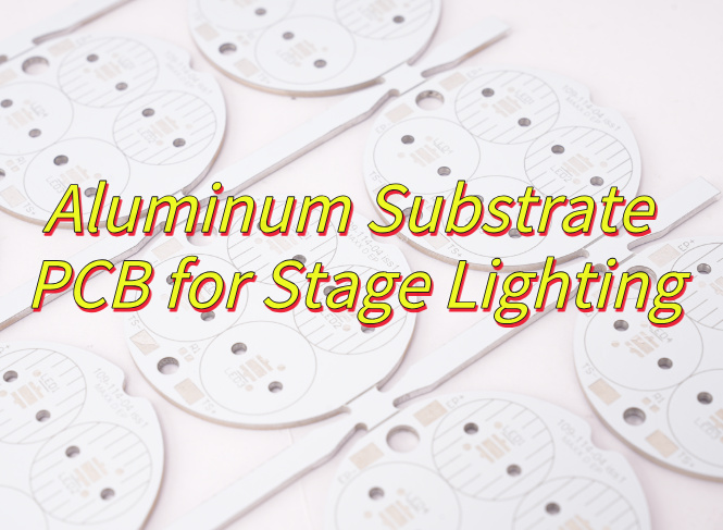
Automotive Aluminum Substrate LED PCB plays an important role in modern vehicle lighting, offering high performance, heat management, and durability. These boards are the backbone of reliable automotive LED systems, meeting the strict demands of harsh driving conditions. In this guide, we will explore what they are, their features, design tips, quality assurance steps, and why choosing the right supplier makes all the difference.
EBest Circuit (Best Technology) has provided custom automotive aluminum substrate LED PCB solutions since 2006. We believe a long-term and stable business relationship with customers is based on our higher quality, more prompt quoting, turnkey EMS LED light PCB board making, and fast delivery service. No matter whether you need our DFM analysis for LED PCB board design, or need custom LED PCB prototypes, or wholesale automotive LED PCB fabrication, or the SMT automotive LED PCB pricelist, we are always available to support you. Just give us your Gerber files and tell us the other special requirement, the quantity you want to order from us, via sales@bestpcbs.com.
What is Automotive Aluminum Substrate LED PCB?
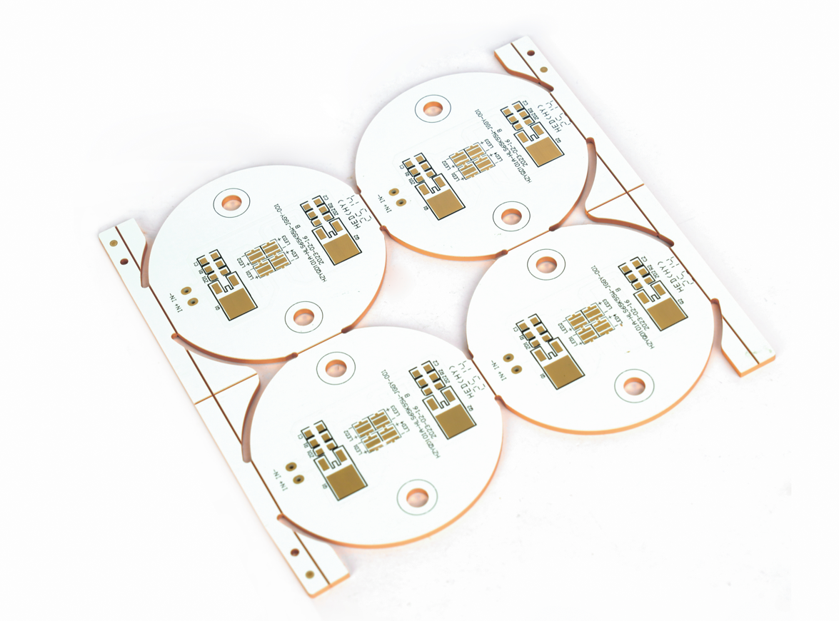
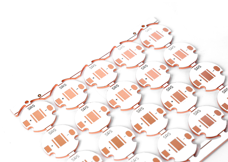
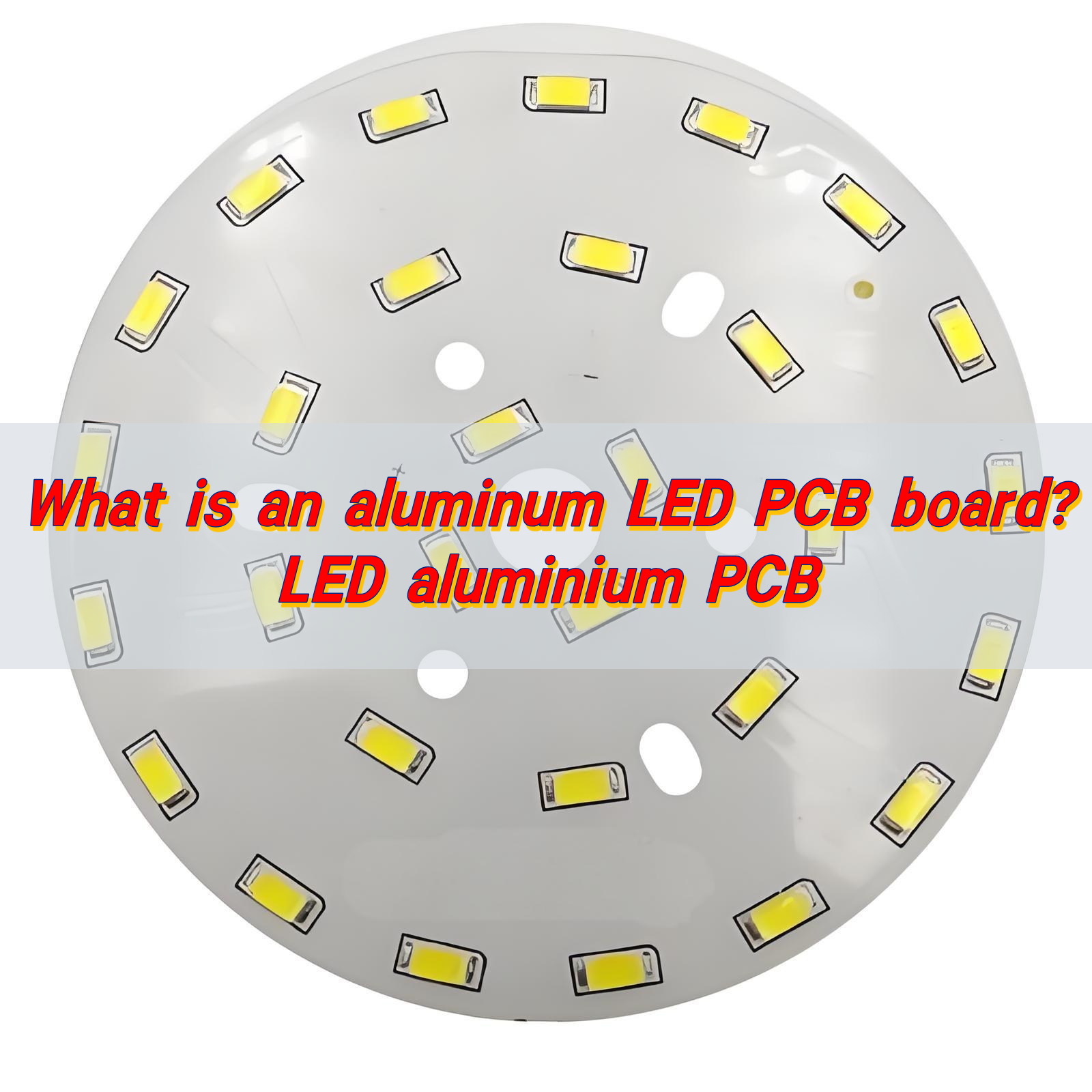
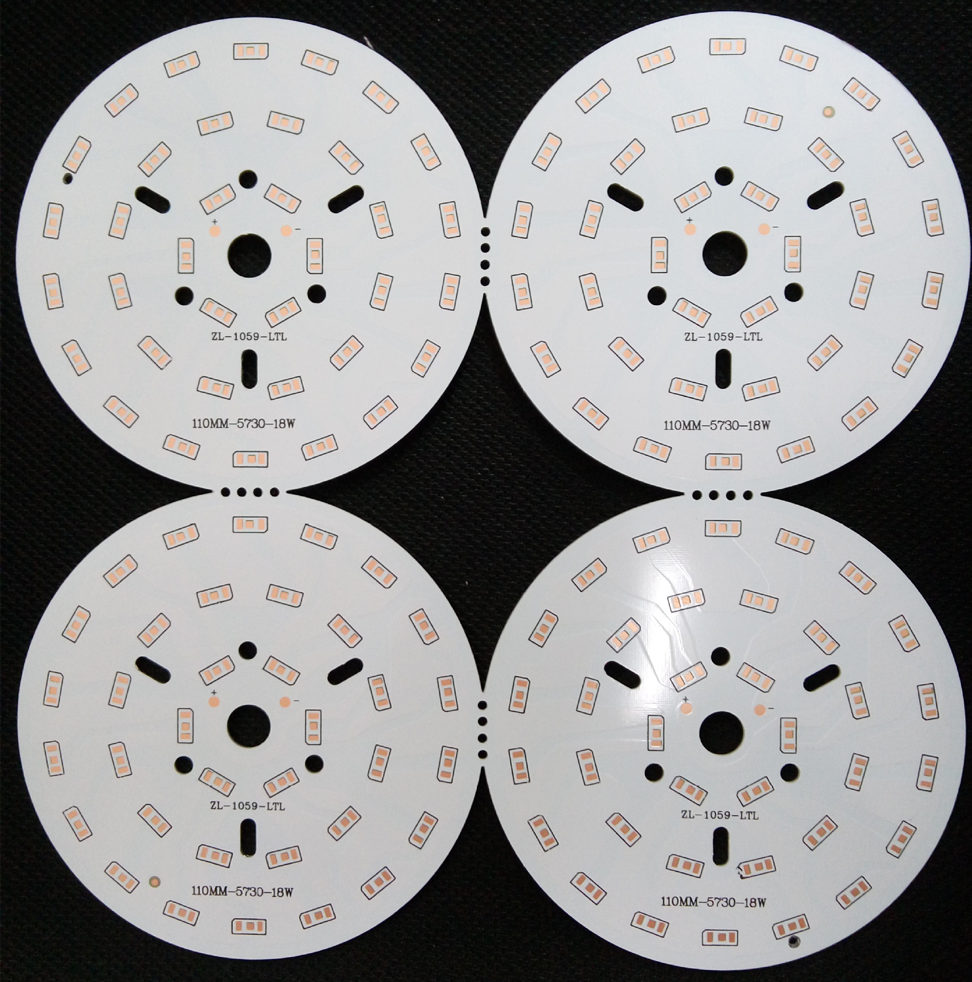
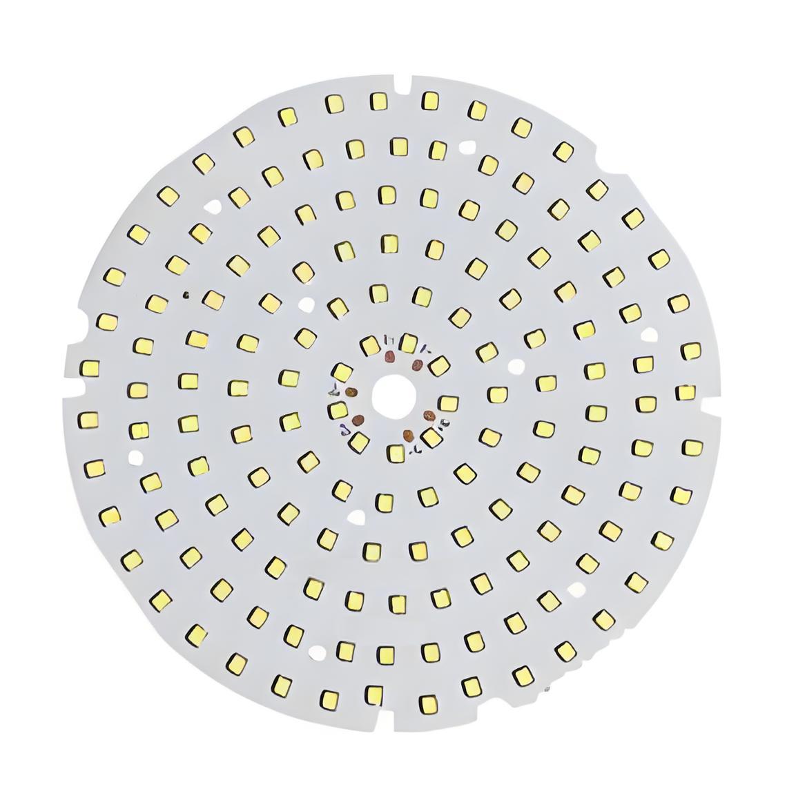
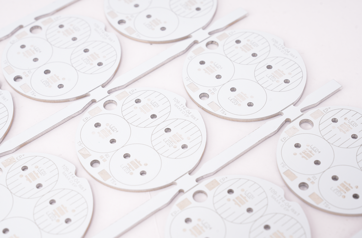
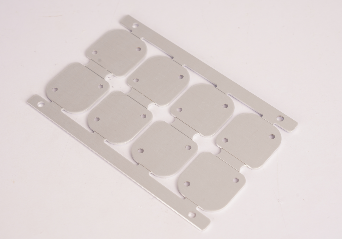
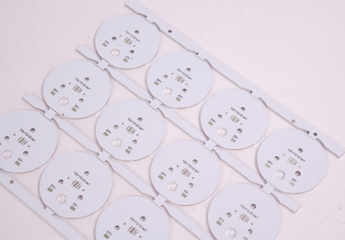
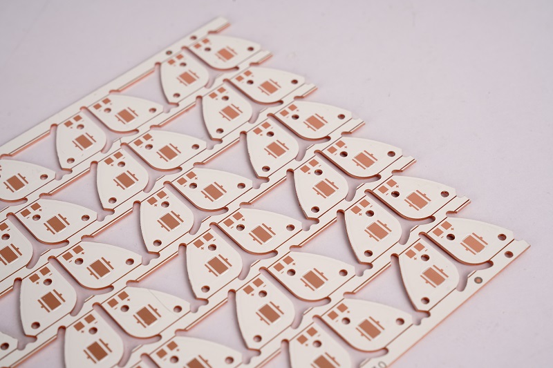
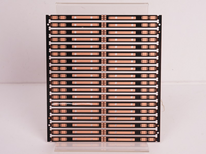
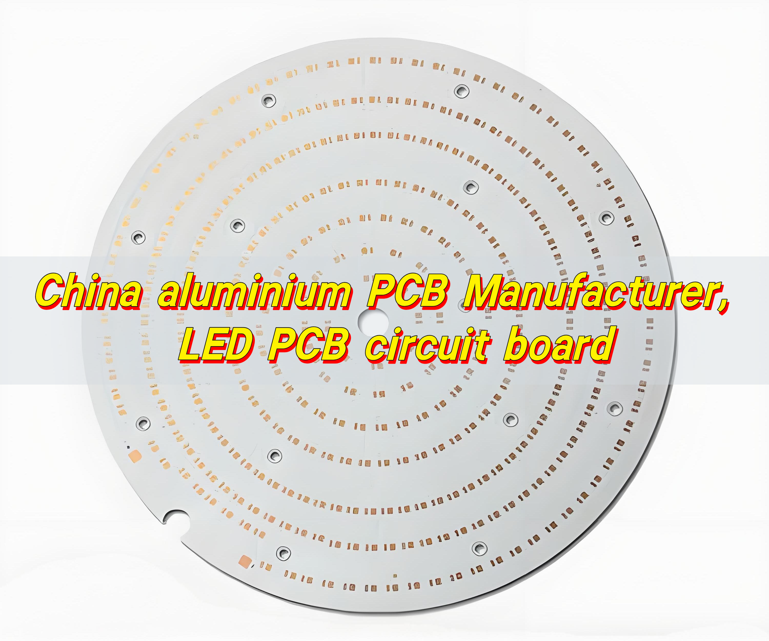
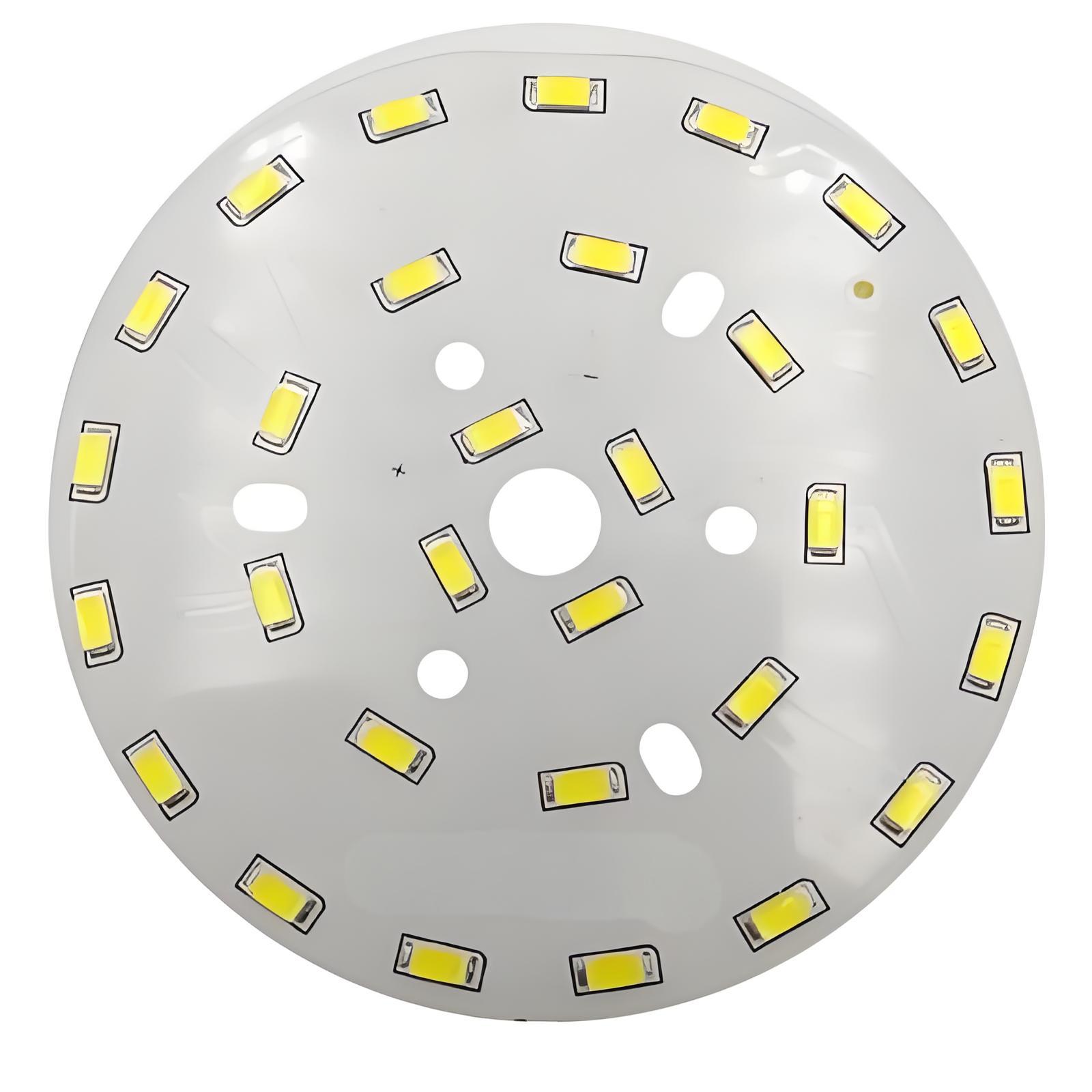
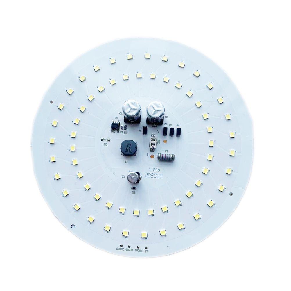
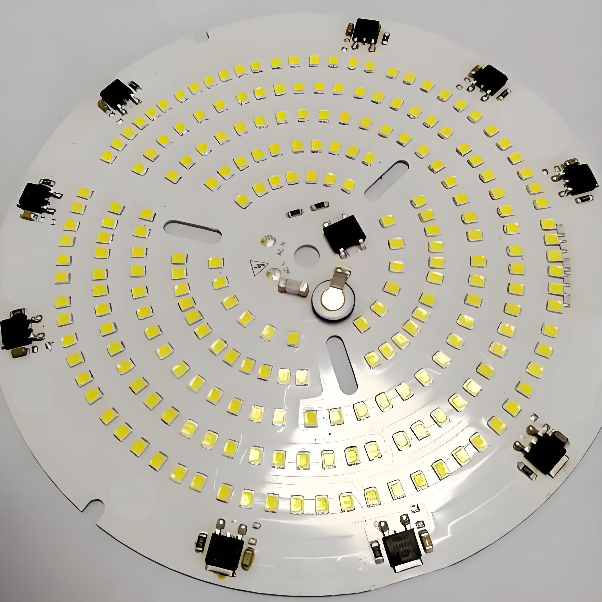
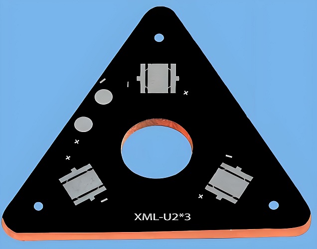
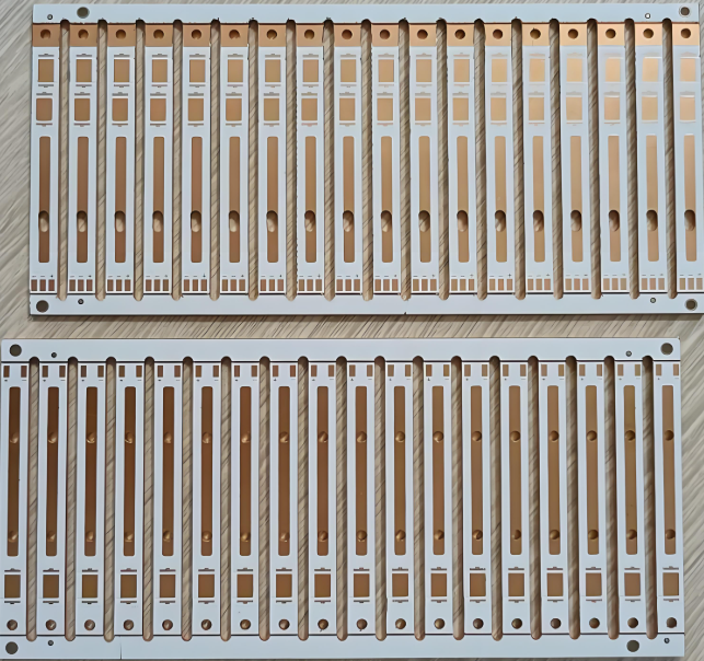
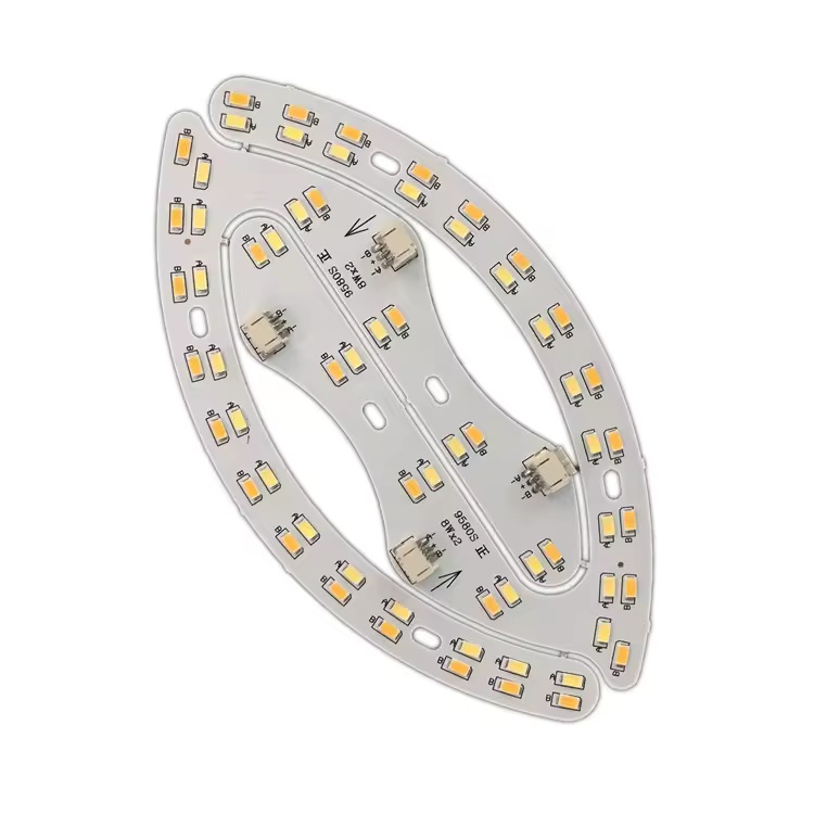
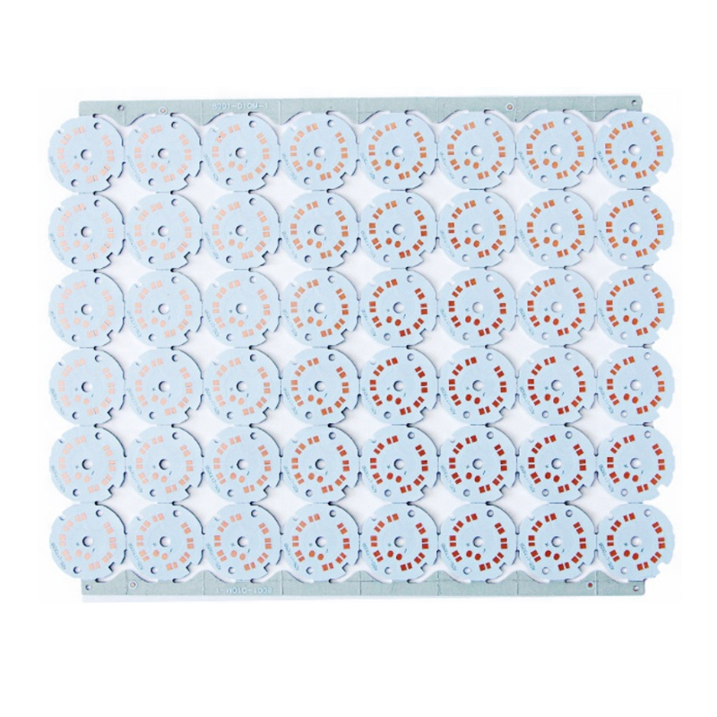
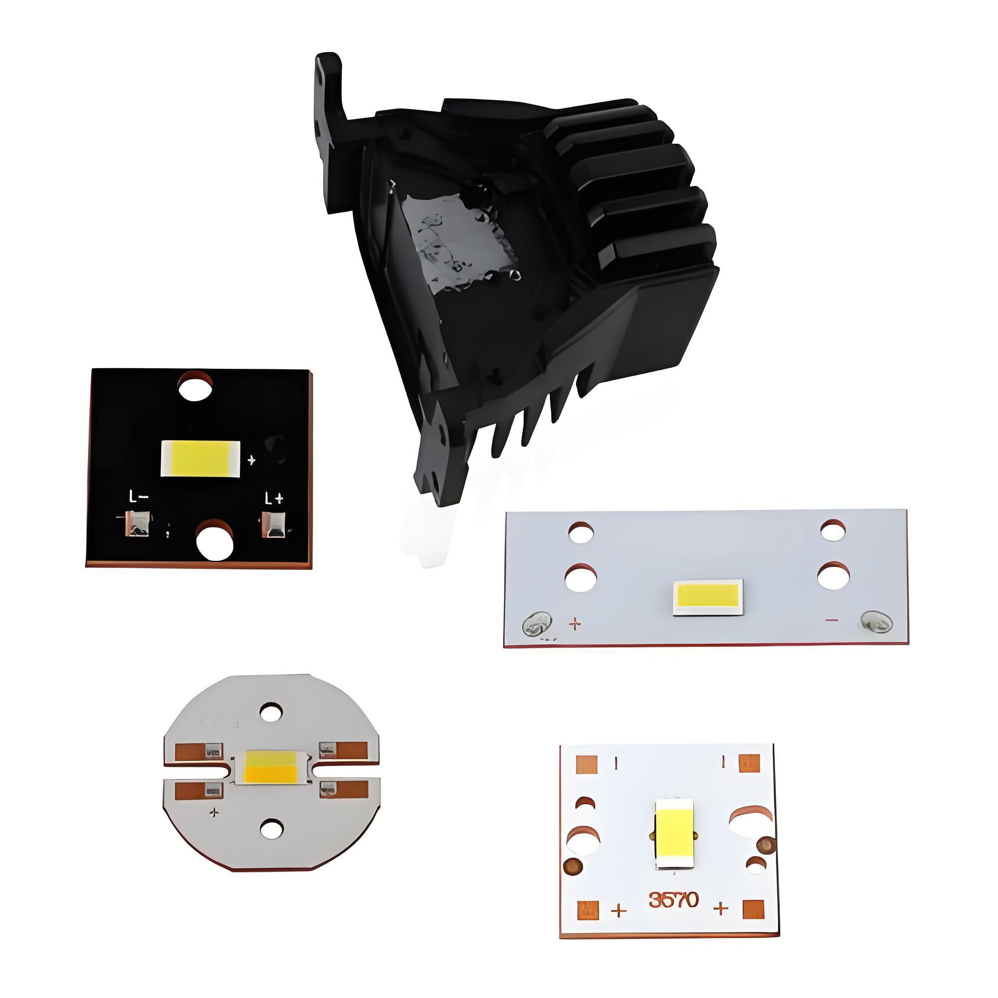
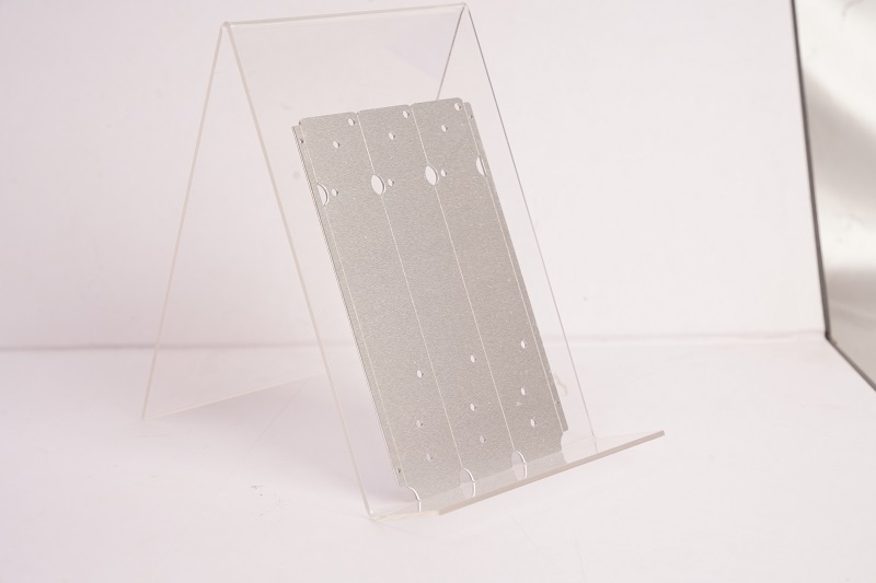
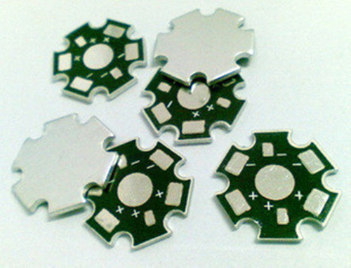
An automotive aluminum substrate LED PCB is a specialized circuit board built on a three-layer structure: a copper circuit layer, a thermally conductive but electrically insulating layer, and a metal base layer made of aluminum. This design combines reliable electrical performance with efficient heat management. The insulating layer plays a major role in transferring heat from the LEDs to the aluminum base, preventing direct electrical contact while enabling rapid thermal dissipation.
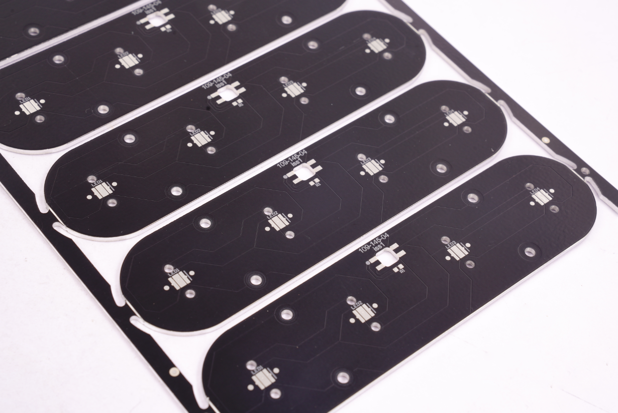
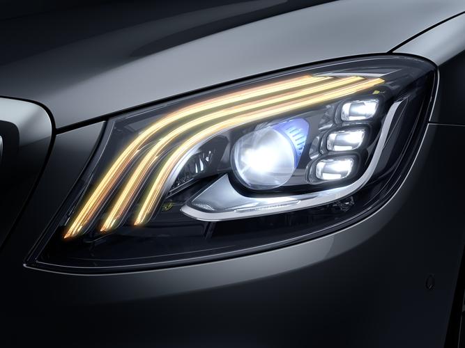
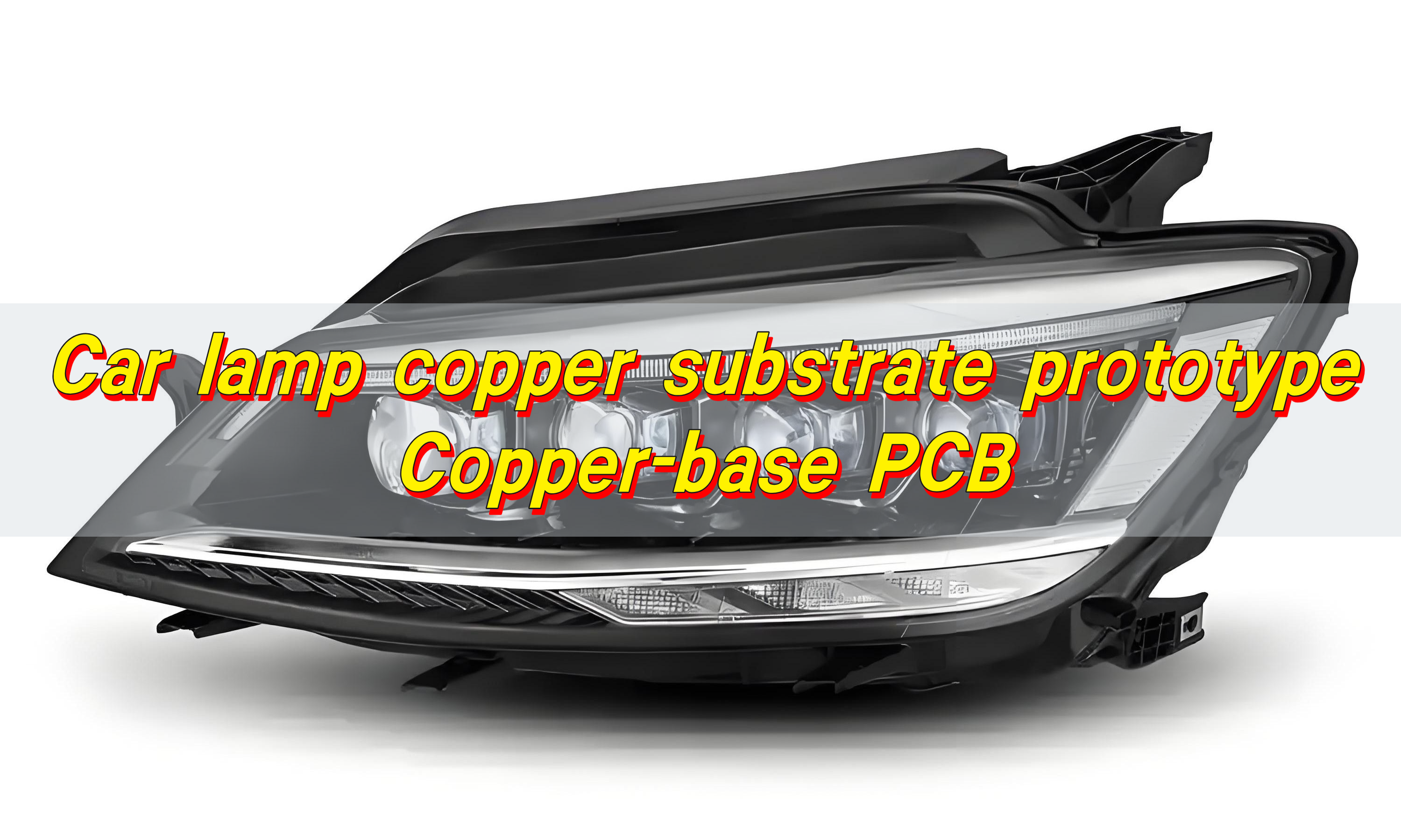
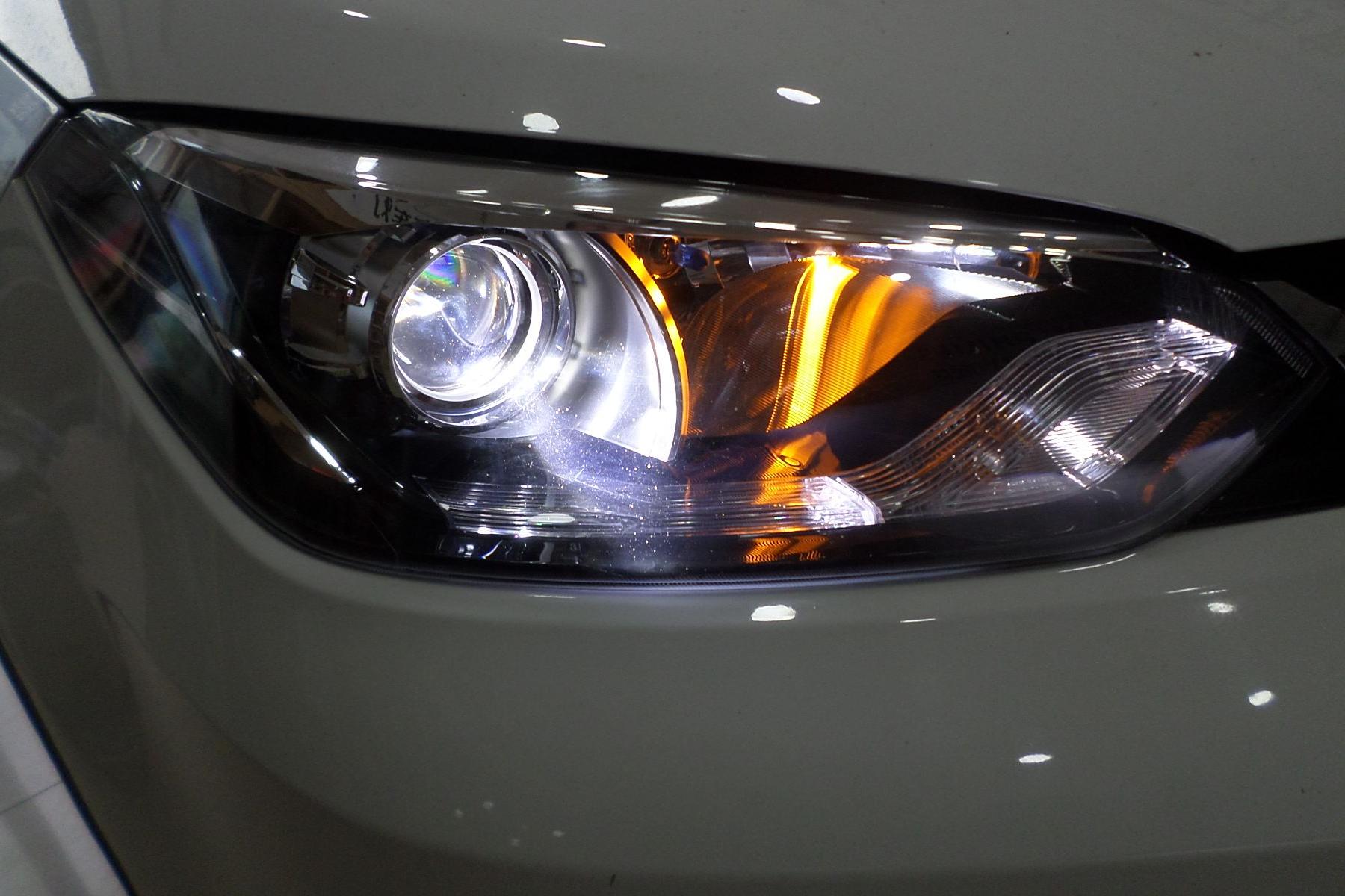
These PCBs are generally used in high-power automotive LED lighting such as headlights, brake lights, and interior lamps. Beyond lighting, they are also applied in vehicle electronic regulators, ignition systems, and other heat-sensitive automotive electronics. By stabilizing temperatures and reducing thermal stress, automotive aluminum substrate LED PCBs help extend component lifespan and maintain consistent performance even in demanding driving conditions.
What are the Features of Automotive Aluminum Substrate LED PCB?
Automotive Aluminum Substrate LED PCBs in particular stand out for their thermal conductivity, mechanical strength, and vibration resistance. The aluminum base supports heavier components without warping, while also protecting circuits from road shock. They also provide better dimensional stability under temperature changes, which is extremely vital for automotive lighting exposed to varying climates. Corrosion-resistant coatings can further enhance reliability in wet or salted environments.
Tips for Optimizing Aluminum PCB Design for Automotive LED
Designing an aluminum PCB for automotive LEDs requires balancing heat dissipation, electrical performance, and mechanical fit. Here are some great tips:
- Use proper thermal vias to enhance heat transfer to the aluminum base.
- Keep LED spacing consistent to avoid uneven light output.
- Select solder masks and surface finishes rated for high temperatures.
- Account for enclosure space early in the design to ensure secure mounting.
How does Automotive LED PCB Factories Ensure the PCB LED Quality?
- Material Selection – Use high-grade aluminum cores with stable thermal conductivity for reliable heat performance.
- Precision Manufacturing – Properly maintain tight process control to ensure circuit accuracy and consistent layer bonding.
- Automated Optical Inspection (AOI) – Detect surface defects and alignment issues early in production.
- X-ray Testing – Check solder joints, hidden pads, and internal connections for integrity.
- Thermal Shock Testing – Simulate rapid temperature changes to assess stability.
- Vibration Testing – Ensure mechanical durability under road conditions.
- Corrosion Resistance Testing – Evaluate performance in moisture, salt spray, or chemical exposure.
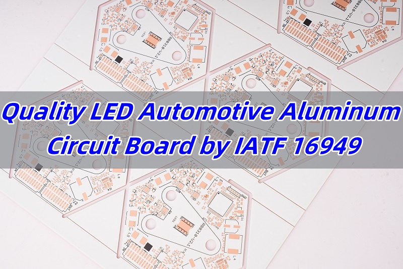
- Compliance with IATF 16949 – Follow automotive-grade quality management to deliver consistent, high-reliability PCBs.
How to Select the Right Aluminum PCB Board for Your LED Projects?
- Assess LED Power Requirements – Higher-power LEDs need boards with higher thermal conductivity to manage heat effectively.
- Consider the Operating Environment – Outdoor or engine-compartment lighting requires materials that withstand high temperatures and humidity.
- Choose the Right Copper Thickness – Use thicker copper layers for high-intensity headlights; standard thickness is fine for interior or decorative lighting.
- Select Suitable Coating Types – Apply sealed coatings for outdoor or harsh conditions; use simpler finishes for indoor environments.
- Balance Cost and Performance – Match technical needs with budget without compromising reliability and safety.
How to Choose the Best Aluminum PCB Enclosure for Harsh Automotive Environments?
- Check the Protection Level – Select IP-rated enclosures to shield against moisture, dust, and debris in external automotive lighting.
- Choose Durable Materials – Use aluminum enclosures with anti-corrosion treatment for extended service life in varied climates.
- Support Heat Management – Opt for designs that allow airflow or include thermal pads to maintain LED efficiency.
- Match to Application Needs – Ensure the enclosure fits the space and mounting requirements of the vehicle’s lighting system.
- Verify Mechanical Strength – Confirm the enclosure can withstand vibration and impact from road conditions.
Why Choose EBest Circuit (Best Technology) for Making Automotive Aluminum Substrate LED PCB?
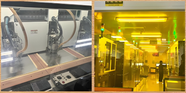
Consistent Product Quality – Strict quality control systems eliminate common issues such as uneven finishes or faulty connections. With sophisticated inspection systems, there is strict QC on each manufacturing process.
Fast Production Timelines – Optimized workflows ensure quick turnaround without compromising reliability. Even in the peak season, we could ensure your order is produced on schedule. Our production and the SMT lines are running 24/7.
Advanced Material Selection – Use of high-grade aluminum substrates with stable thermal conductivity for better heat management. We provide the EMS turnkey services from material procurement to final delivery.
Expert Engineering Support – Designs are optimized for thermal performance, mechanical strength, and automotive durability. Any inquiry, pls send us at sales@bestpcbs.com. We will support the DFM analysis freely.
Industry Certifications – ISO9001, ISO13485, IATF16949, and AS9100D compliance proves capability to meet strict automotive and industrial standards. Our customers come from a broad range of industries. Our comprehensive industry certifications empower cross-industry collaborations from medical devices to automotive electronics with rigorous quality assurance.
Whether you need prototypes or mass production, we provide high-reliability automotive aluminum substrate LED PCBs that help your projects succeed in competitive markets. By working closely with your design team, we ensure every PCB meets your exact requirements, reducing rework and improving final product performance. Show us your inquiry details at sales@bestpcbs.com. We will be more than happy to give you our best service and the best quotes.