Today let us explore everything about SMD LED PCB, their advantages, design tips, and the main differences between SMD LED and COB LED PCBs together.
At Best technology, we focus on one stop solution PCB solution for SMD LED PCB over 18 years, and we have a SMT patch line that can support mass production with fast delivery. And we can provide you PI Analysis, SI Analysis, EMC Testing with the SMD LED PCB you designed. Then we can provide you with one piece MOQ rapid prototyping at 24-72 hours delivery. Welcome to contact us sales@bestpcbs.com if you have any request for SMD LED PCB.
What Is SMD LED PCB ?
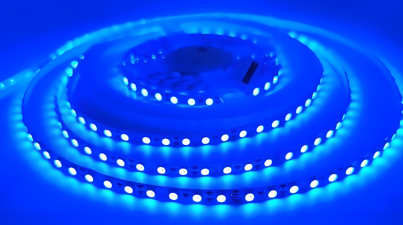
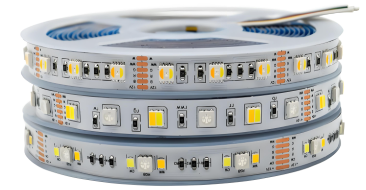
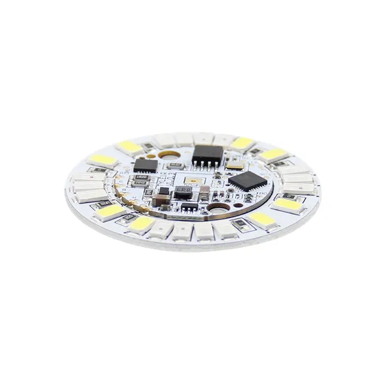
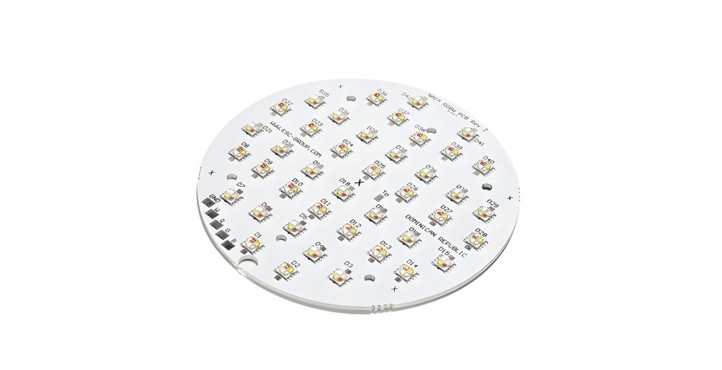
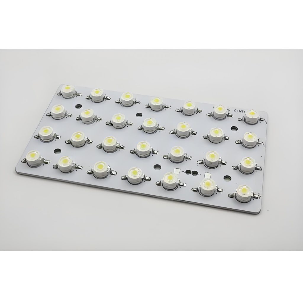
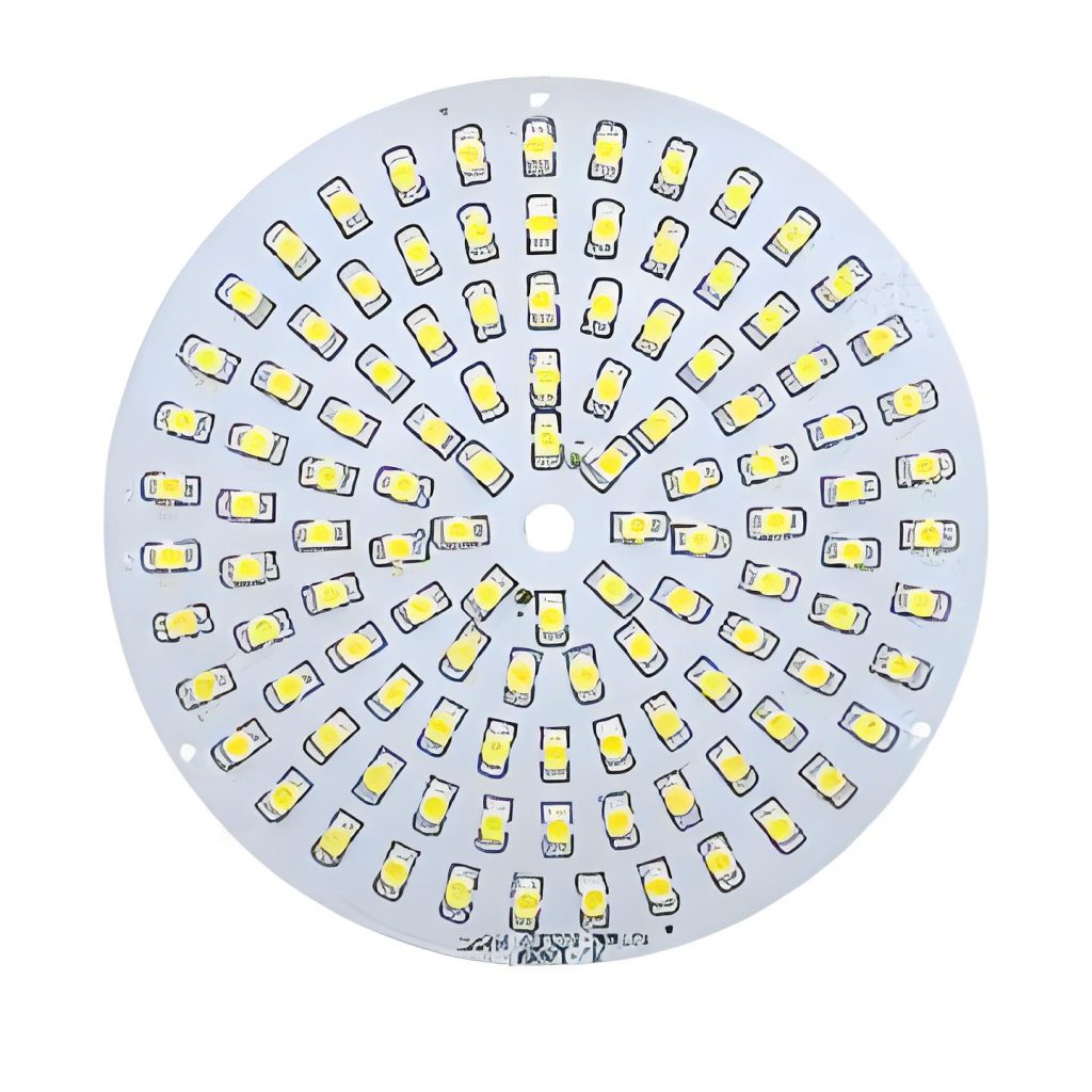
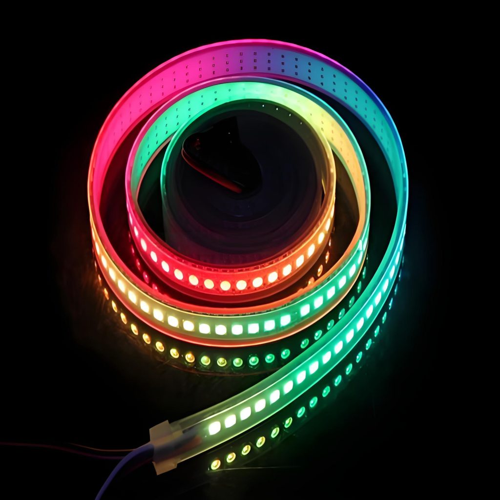
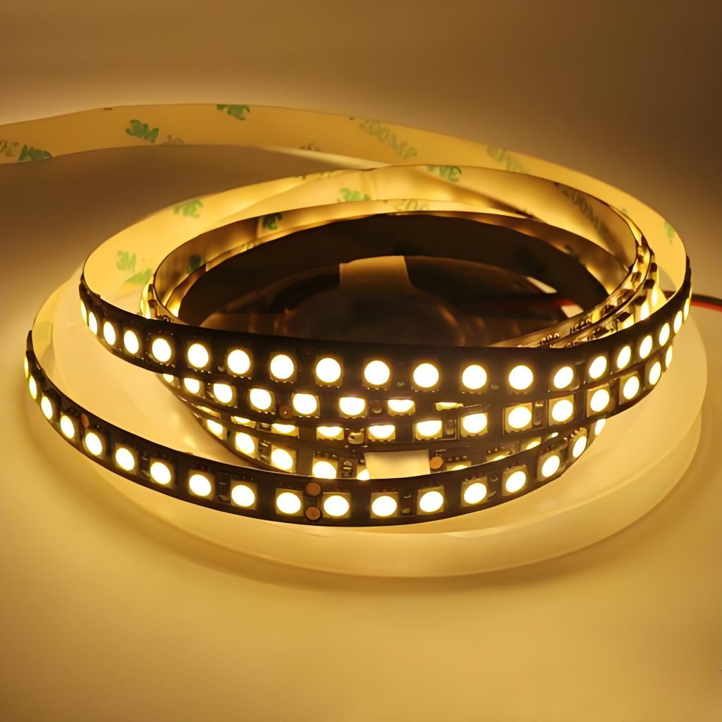
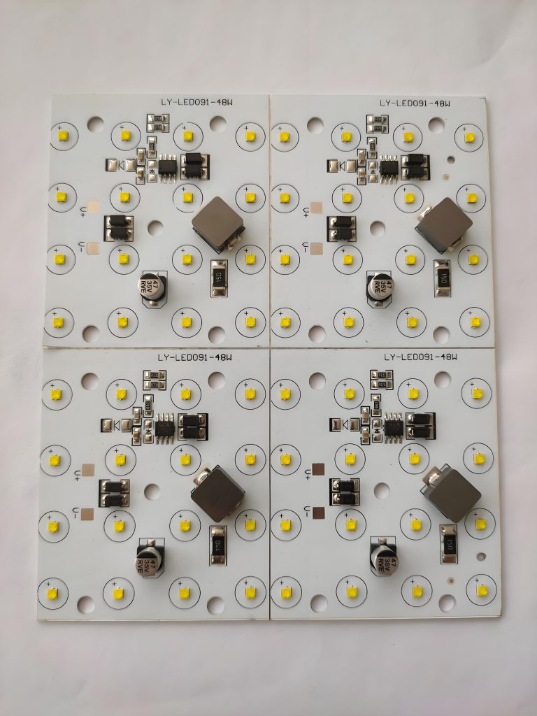
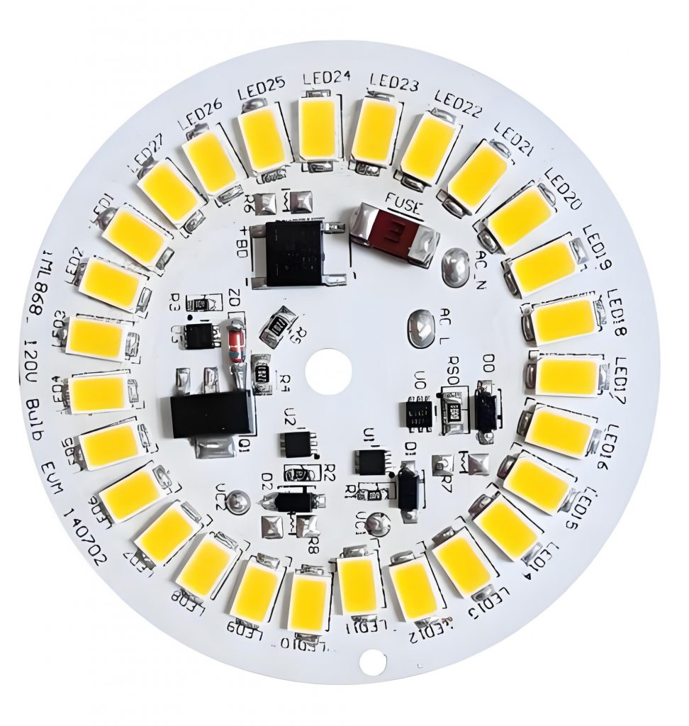
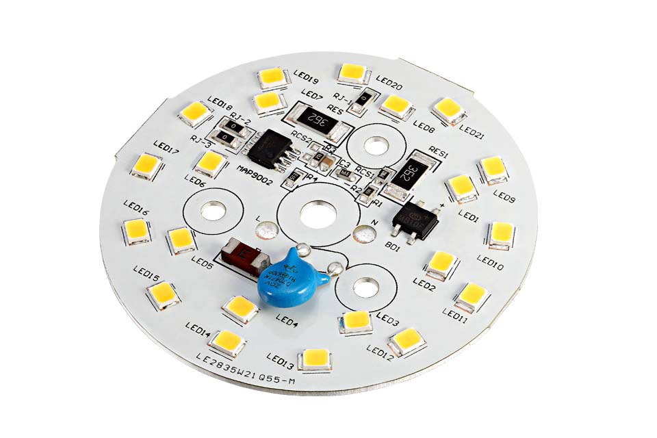
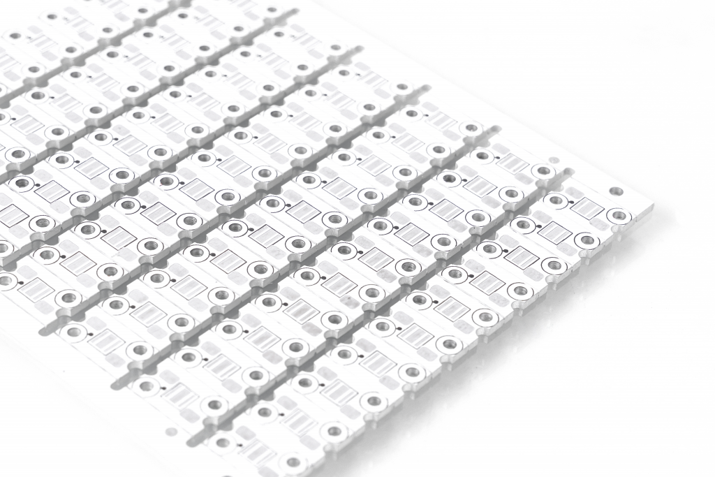
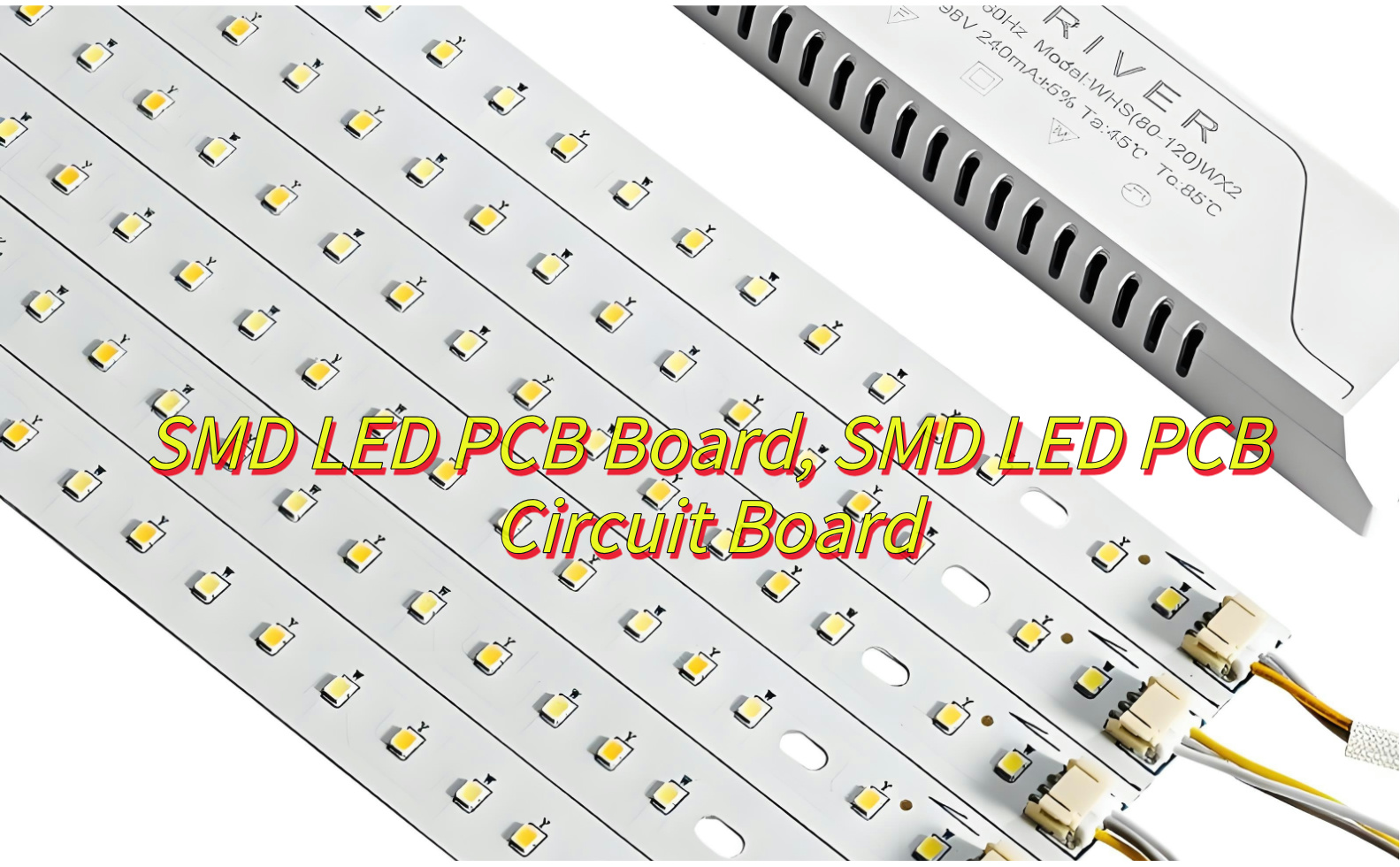
SMD LED PCB, or Surface-Mounted Device Printed Circuit Board, is designed specifically for mounting and connecting SMD LEDs, which are compact and efficient light sources. Unlike traditional through-hole LEDs, SMD LEDs are mounted directly onto the surface of the PCB, saving space and enabling more intricate designs. These boards are commonly used in modern electronics, offering versatility in applications like lighting, displays, and automotive systems.
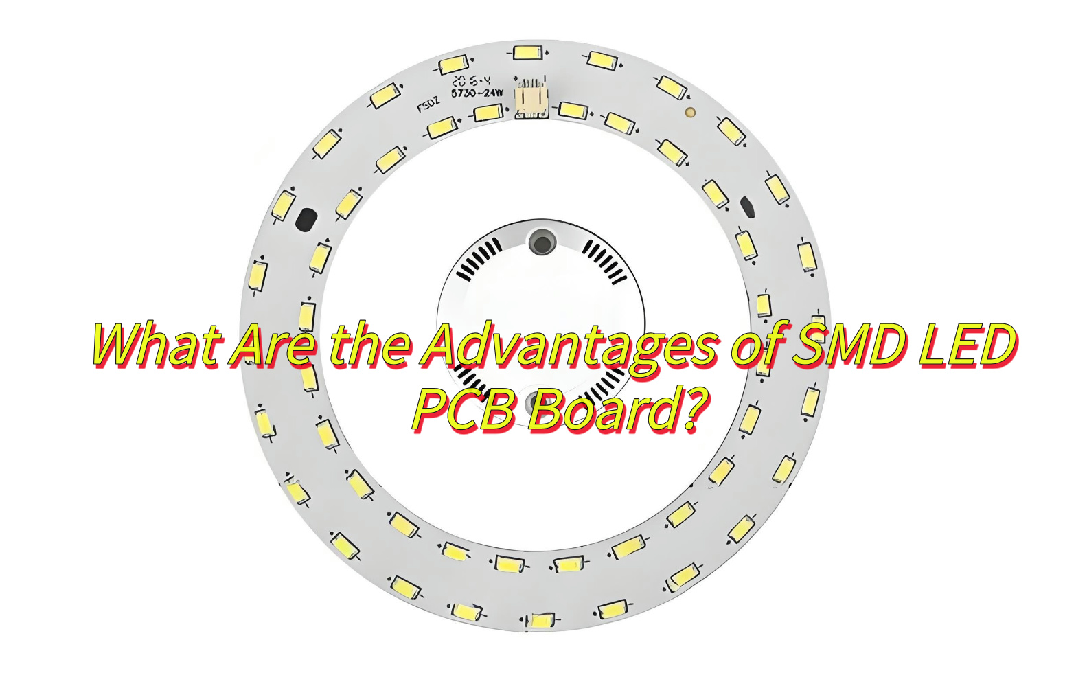
What Are the Advantages of SMD LED PCB Board?
- Space Efficiency: 50–70% smaller than traditional through-hole LED designs.
- High Brightness: Achieves 100–200 lumens per watt (e.g., Samsung LM301B SMD LEDs).
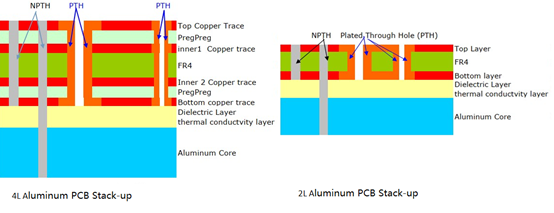
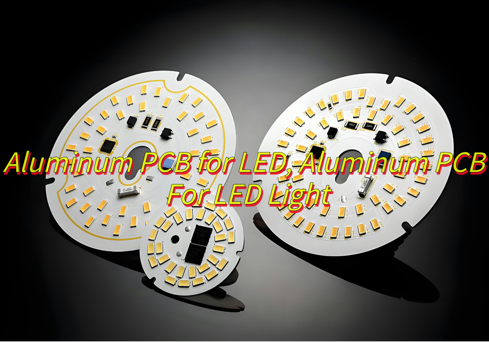
- Thermal Management: Aluminum-core PCBs reduce junction temperatures by 15–25°C vs. FR4.
- Energy Savings: 30–50% lower power consumption than COB LEDs in task lighting.
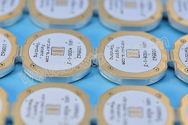
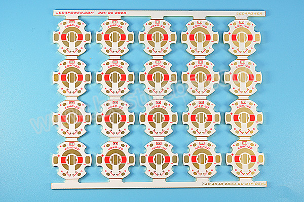
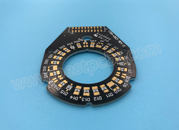
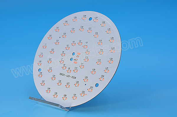
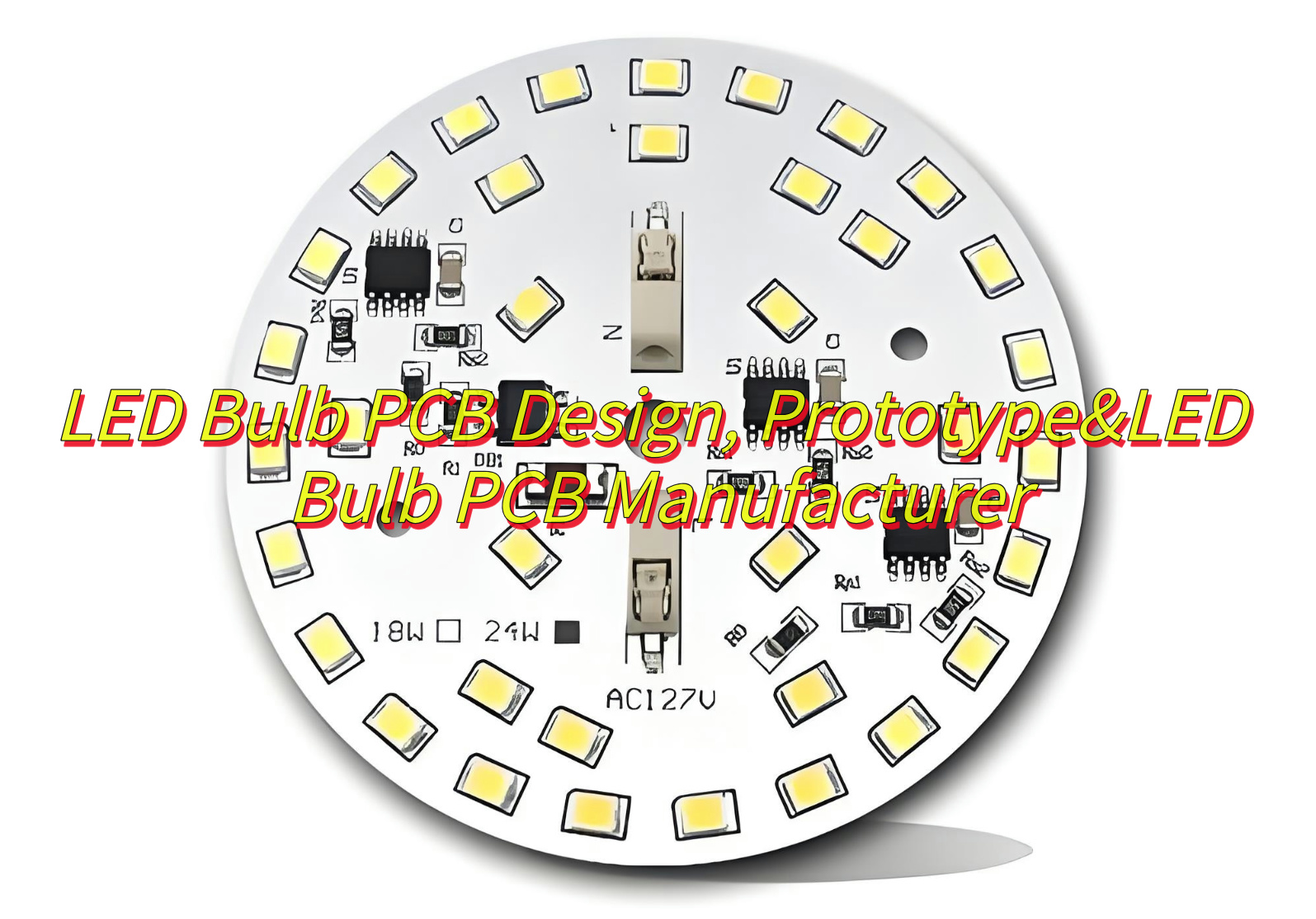
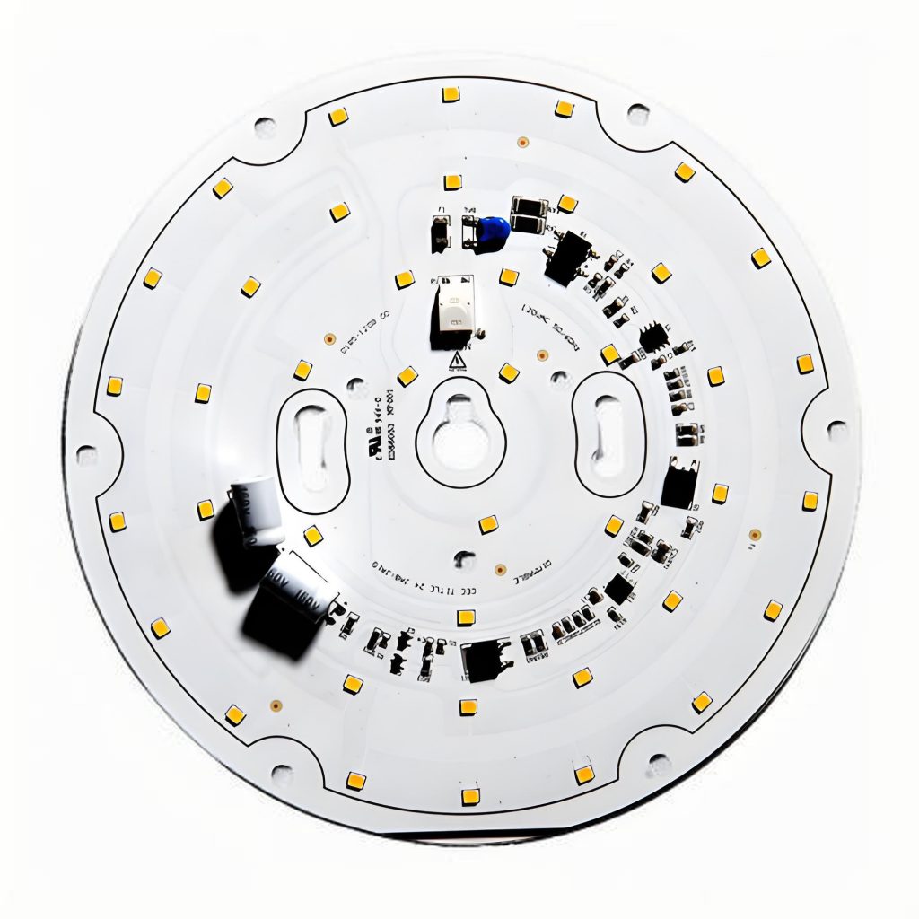
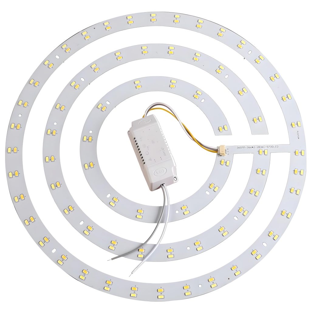
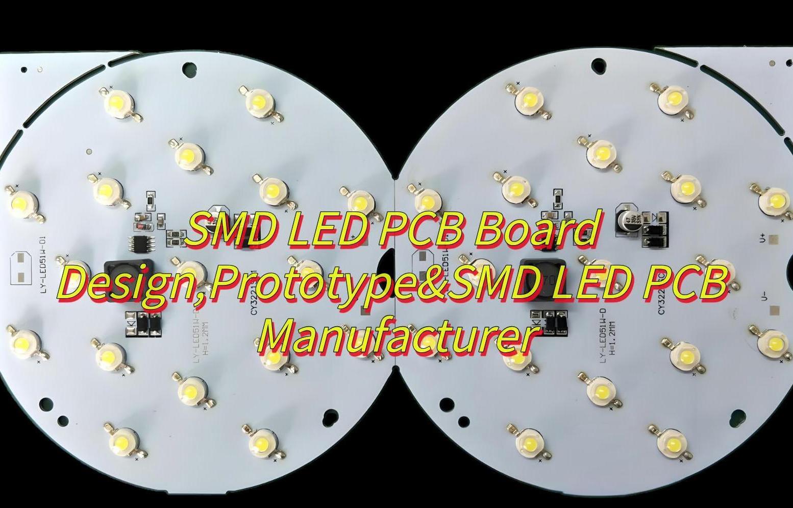
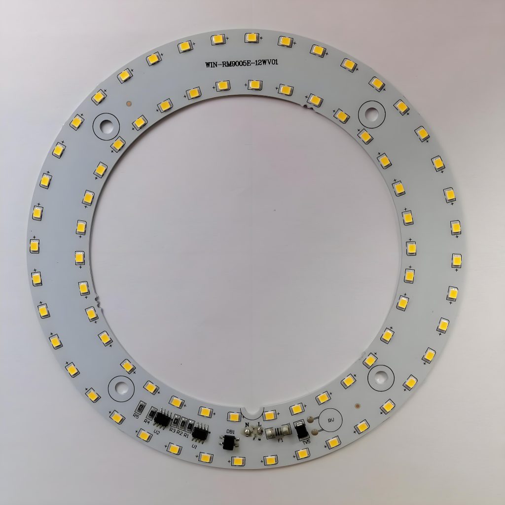
- Design Flexibility: Supports circular, hexagonal, or custom-shaped boards.
What Are the Disadvantages of LED SMD PCB?
- Poor heat dissipation-low power is prone to overheating, high power requires aluminum substrate, but the price is high.
- Difficult to repair-dense patches, replacement of easily damaged peripherals.
- Strict process-precision equipment is required, manual soldering is prone to false soldering.
- Easy to damage-lamp beads are exposed, afraid of collision and bending.
- Uneven light-grainy, poor brightness.
- Not resistant to dirt-afraid of moisture and dust, easy to age outdoors.
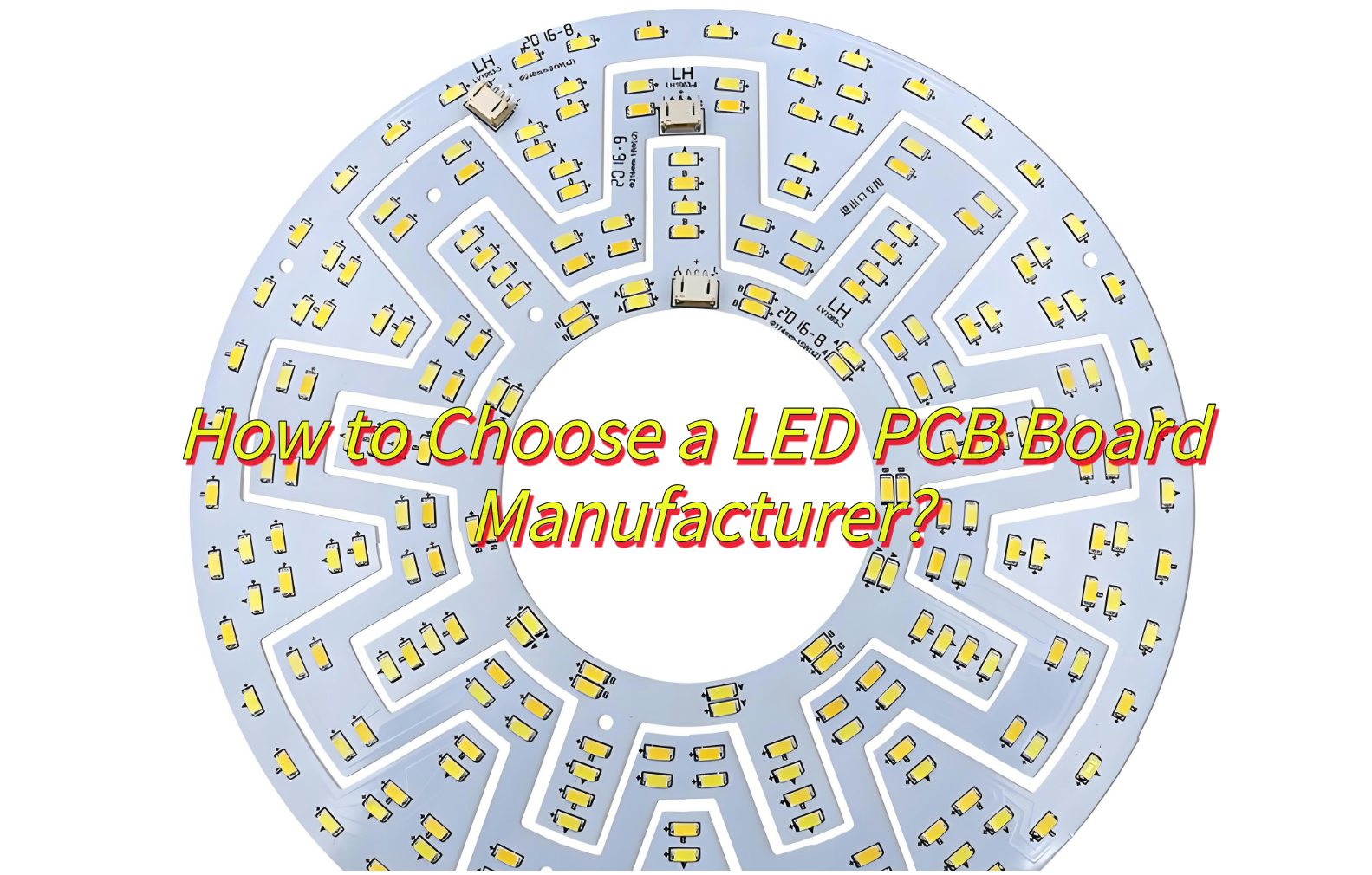
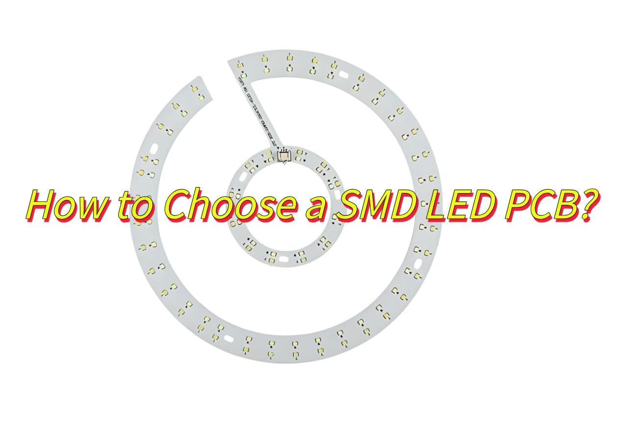
How to Choose a SMD LED PCB?
- Scene Matching: SMD is used in common scenes, such as outdoor advertising and stage rental screens, which are low-cost.
- Material Matching: FR-4 is selected for low power, and aluminum substrate is used for high power/heat dissipation.
- Reliable Process: Precision welding equipment to avoid cold soldering.
- Density Selection: High density (such as P1.2+) is more delicate when viewed up close, and low density saves costs.
- Protection Adaptation: Moisture and dustproof is required outdoors, and simplified protection is required indoors to reduce costs.
How to Design a SMD LED PCB Board?
Here are main steps for SMD LED PCB board design:
1. Thermal Design: Use 1.5–2mm thick aluminum PCBs for >3W LEDs. And add thermal vias under LED pads (0.3–0.5mm diameter).
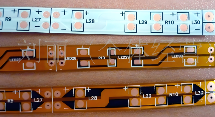
2. Trace Width: 0.5mm traces for 1A current (FR4) / 0.3mm (aluminum).
3. Pad Layout: Match pad dimensions to LED specs (e.g., 2.8×3.5mm for 2835 LEDs).
4. Optical Spacing: Maintain 5–10mm between LEDs to avoid color mixing.
5. Circular PCB Design Tips: Rotate LED placement at 15–30° angles for uniform illumination.

If you have any other issues with SMD LED PCB design, please feel free to leave a message below this blog.
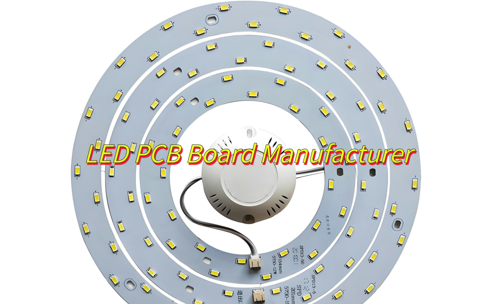
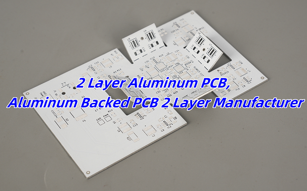
SMD LED PCB Board Manufacturer
As a SMD LED PCB board manufacturer, EBest Circuit (Best Technology), establish on June 28, 2006, is a Hong Kong registered company whom specialize in one stop solution PCB solution for SMD LED PCB. We are dedicated to be your best partner of advance and high-precision SMD LED PCB boards manufacturer. Here are more information about us:
- With SMT patch production line, AOI/X-RAY inspection equipment
- Obtained RoHS, ISO, UL certificates that can promise quality assurance.
- Provide expedited proofing service, and ship within 24 hours at the fastest
- Provide DFM data analysis service, predict problems encountered in design in advance, and reduce production costs
- One-to-one customer service online 24 hours a day to answer your product questions.
If you want to get a quote for your case, please feel free to contact us.
Which is better SMD LED PCB or COB LED PCB?
Packaging method
- SMD: independent lamp bead patch, point light source.
- COB: bare chip integration, surface light source.
Applicable scenarios
- SMD: outdoor advertising screen, stage screen (pitch above P1.25).
- COB: control room, medical screen (micro pitch below P1.25).
Display effect
- SMD: slight graininess, no color difference when squinting.
- COB: no graininess, color deviation may occur when squinting.
Maintenance and protection
- SMD: lamp beads can be replaced individually, but easy to bump.
- COB: fully sealed waterproof and dustproof, need to return to the factory for repair.
Power consumption and cost
- SMD: high power consumption, low cost.
- COB: 20-30% lower power consumption, 50% higher cost.
How Do You Know If a SMD LED Terminal Is Positive or Negative?
- Markings:Look for a green dot, notch, or “+” symbol on the anode.
- Pin Length: The anode (positive) pin is slightly longer in some packages.
- Datasheet Check: Cross-reference the part number (e.g., Cree X-Lamp XM-L2 anode = left pin).
In conclusion, that’s all about SMD LED PCB. At EBest Circuit (Best Technology), we specialize in producing high-quality LED SMD PCBs tailored to your needs, ensuring superior performance and durability. With over 18 years of experience in the industry, our commitment to excellence makes us a trusted partner in PCB manufacturing.