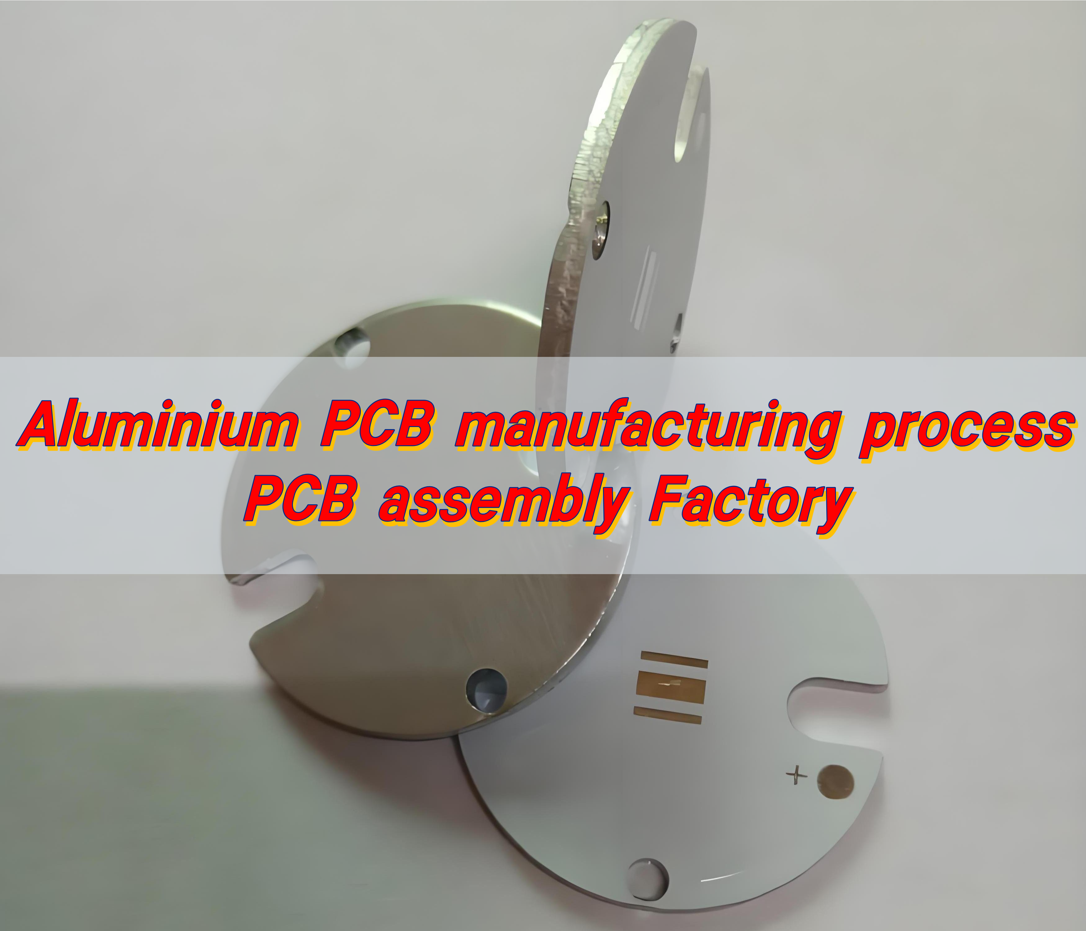
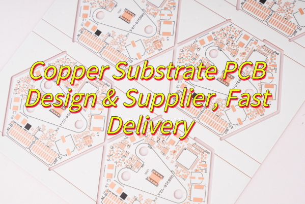
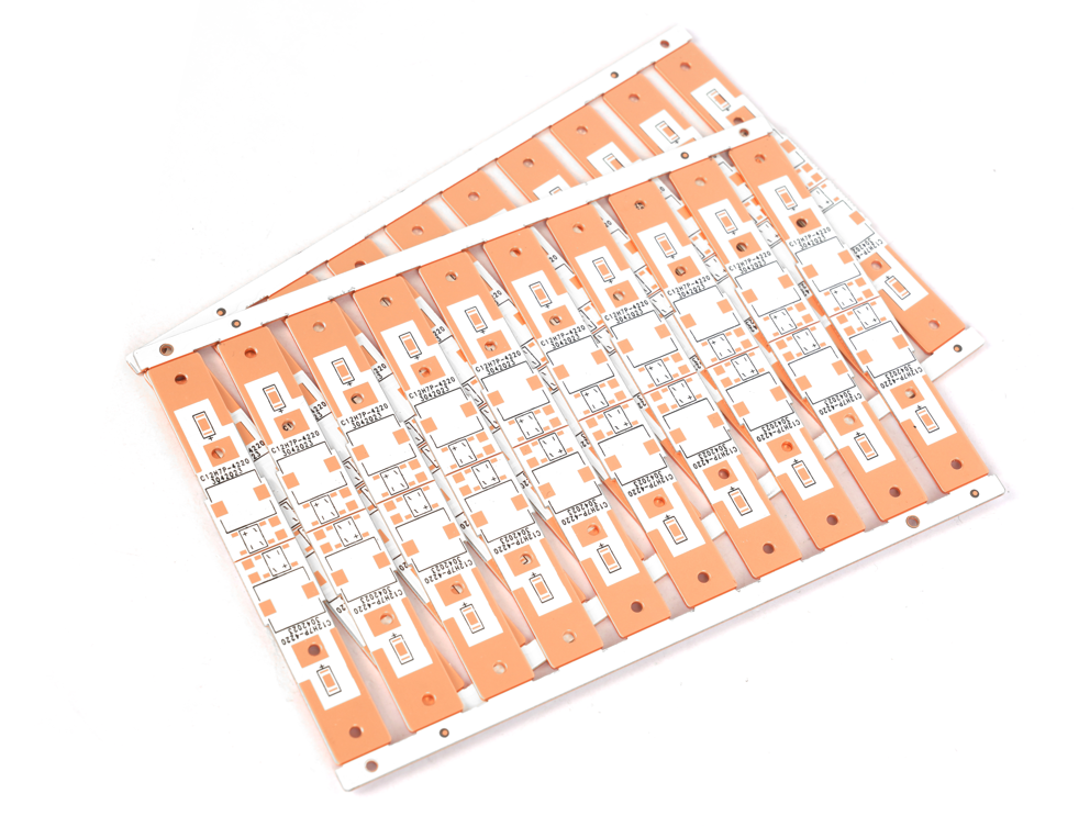
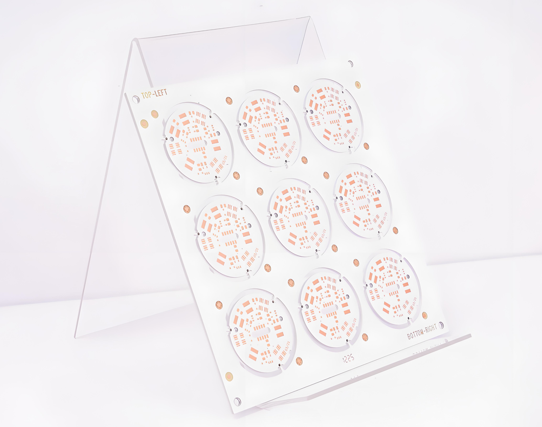
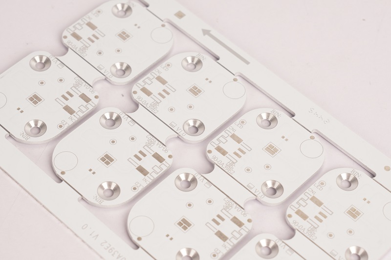
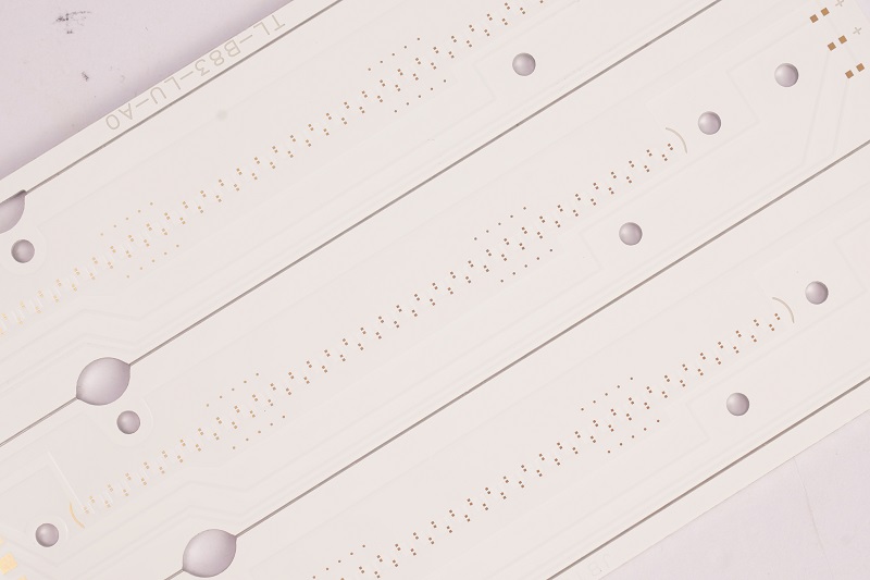
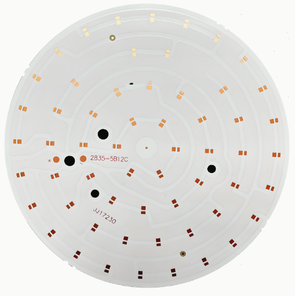
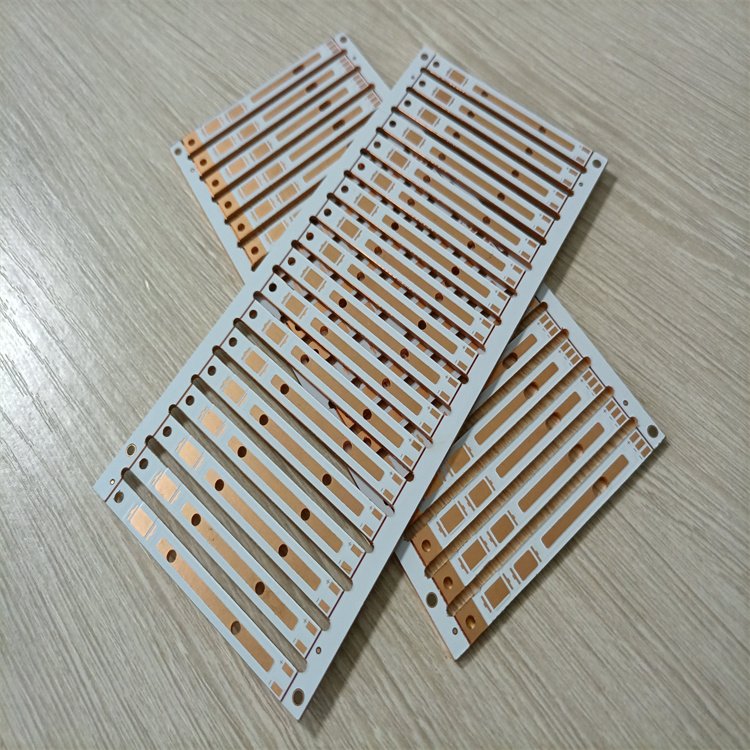
At EBest Circuit (Best Technology) Co., Ltd., we’re experts in MCPCB manufacturing with a complete mcpcb manufacturing process. Our MCPCBs are built to handle tough thermal demands, making them ideal for LED lighting, power converters, automotive modules, and more.
How to make mcpcb?
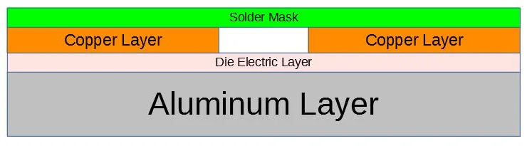
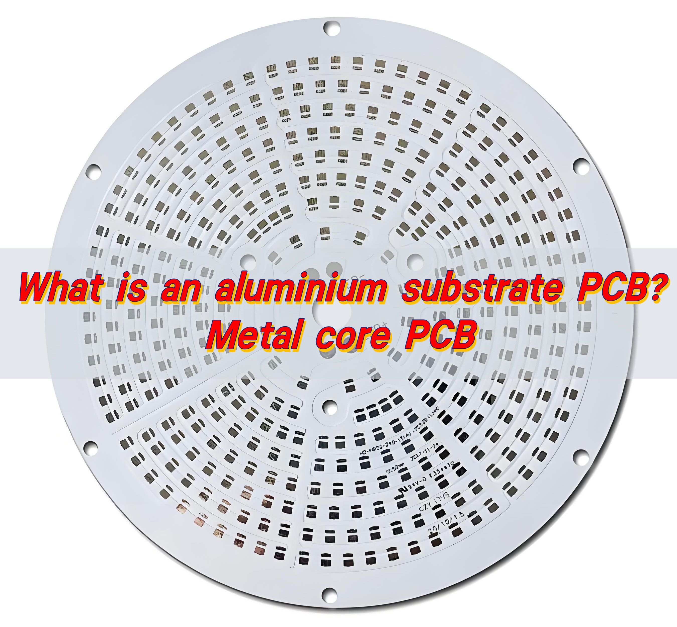
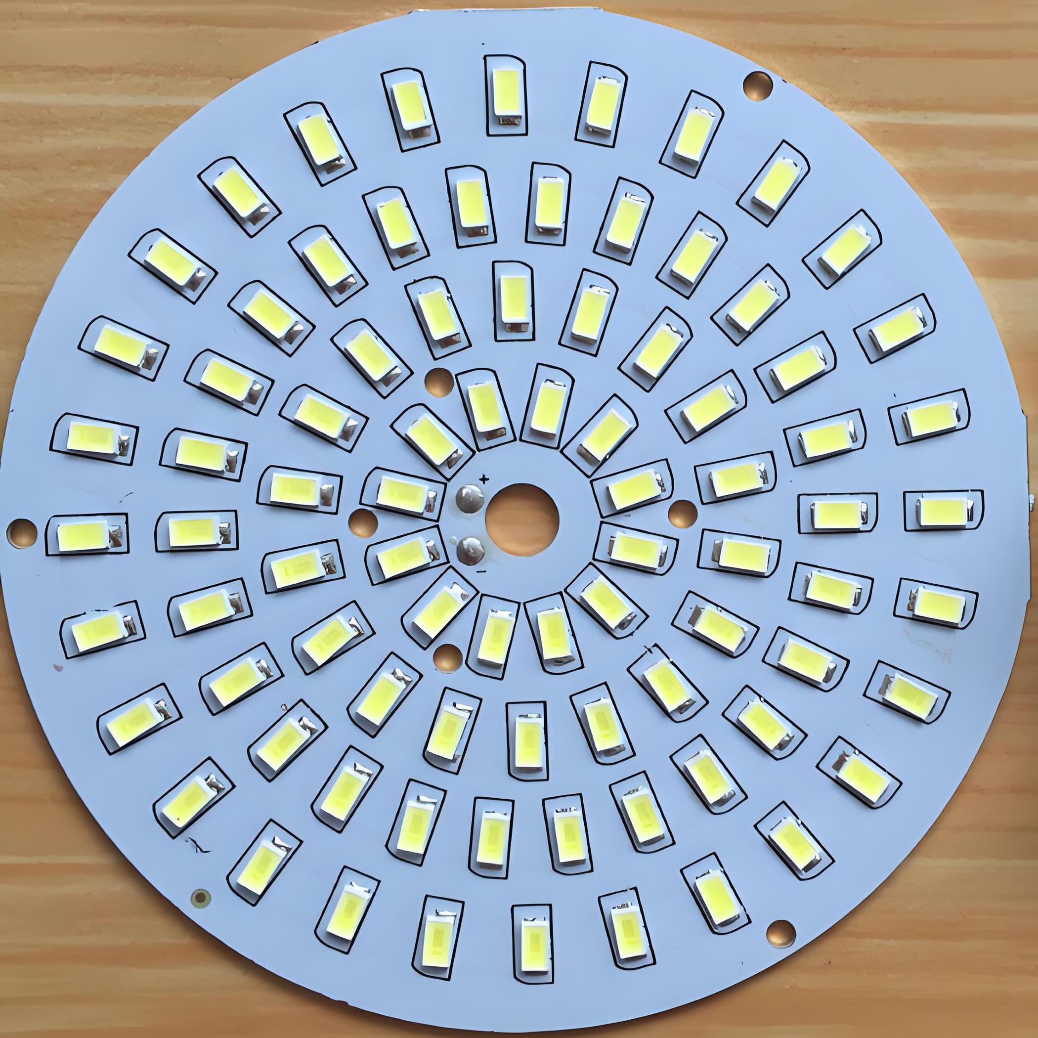
Creating an MCPCB isn’t as simple as layering copper and fiberglass. Instead, it starts with selecting the right base, a metal substrate that replaces the usual FR4 core in traditional boards.
This metal core, usually aluminum or copper, becomes the heart of the MCPCB. It supports components, spreads heat, and provides stability. The process then follows with dielectric layering, circuit etching, drilling, and protective coating.
Every layer and every step is essential to maintain heat control, conductivity, and board longevity.
How is a mcpcb manufactured step by step?
Let’s break the process down into clear steps:
Metal Core Preparation
- A raw aluminum or copper sheet is selected. It’s cleaned and polished to remove oxidation.
Dielectric Layer Application
- A thermally conductive, electrically insulating layer is laminated onto the metal base. This is the key to heat transfer.
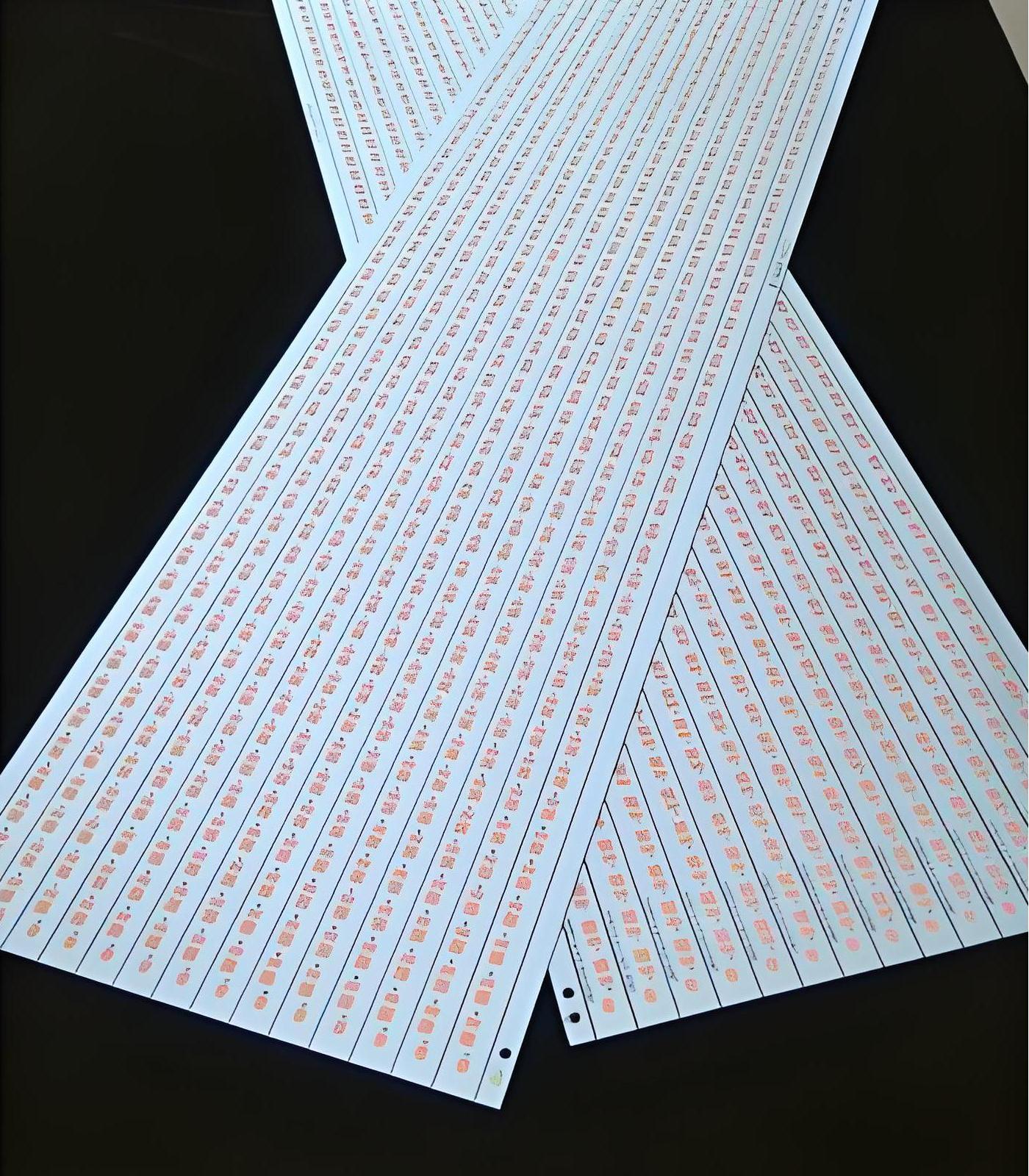
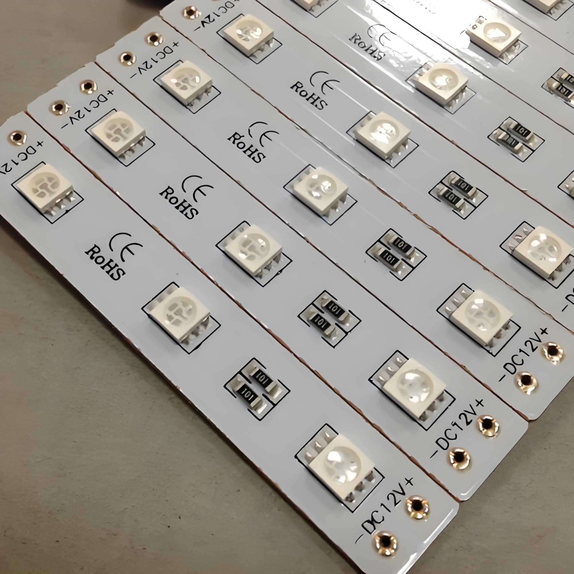
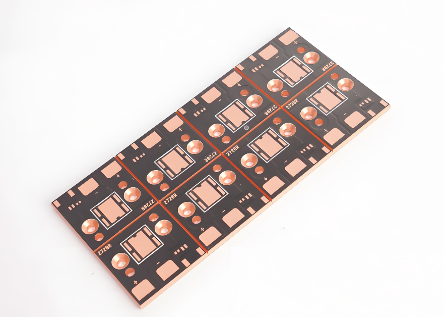
Copper Cladding
- A thin copper foil is laminated on top of the dielectric. This copper layer will carry the circuit patterns.
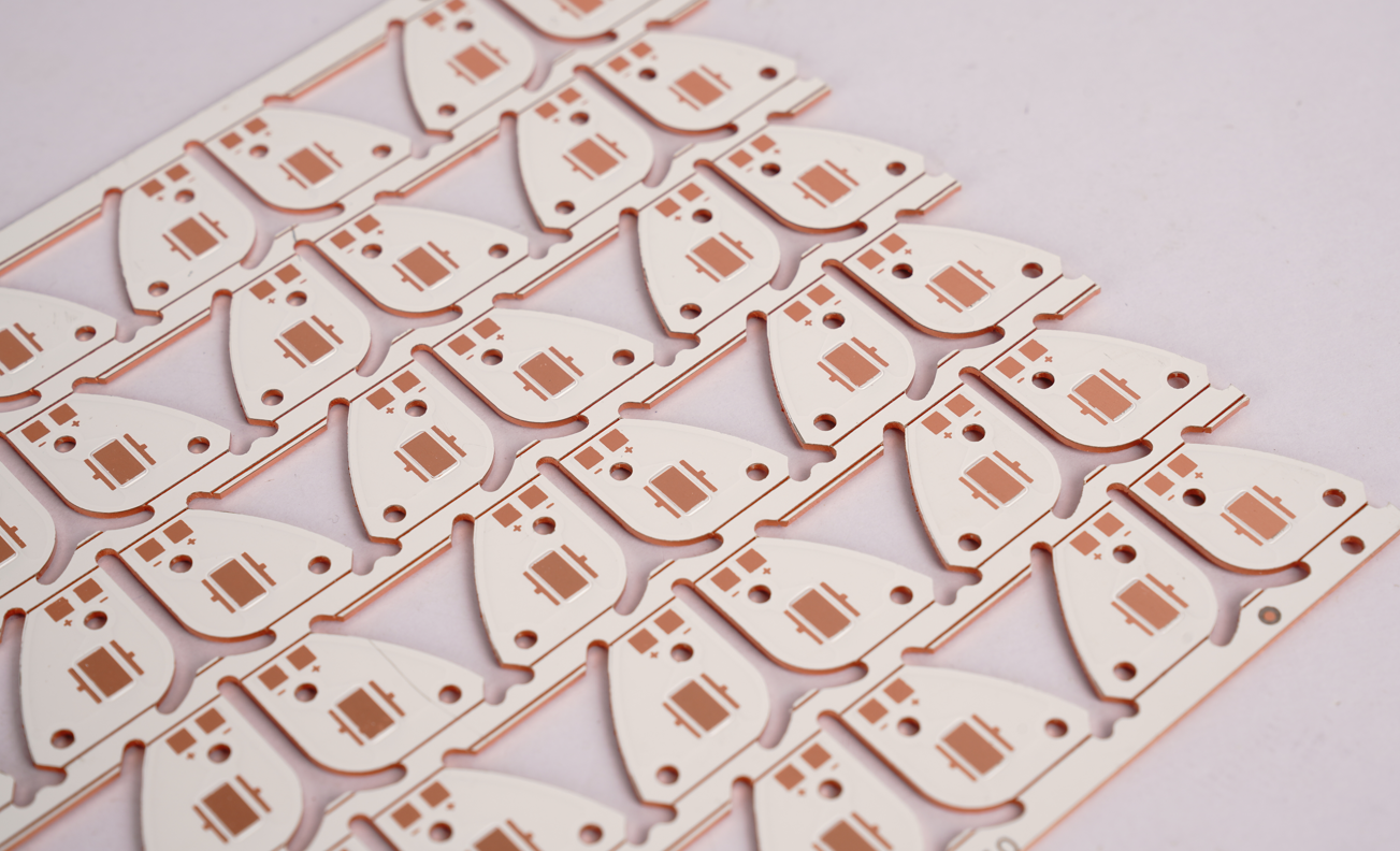
Circuit Imaging and Etching
- Photoresist is applied to the copper surface.
- UV light exposes the circuit design.
- Unwanted copper is etched away, revealing the desired pattern.
Drilling
- Precise holes are drilled for component mounting and vias.
Plating and Solder Mask
- Copper plating reinforces hole walls.
- A protective solder mask is applied, ensuring insulation and component alignment.
Surface Finish
- Finishes like HASL, ENIG, or OSP protect the copper from oxidation and improve solderability.
Testing and Inspection
- Electrical tests, AOI (Automated Optical Inspection), and final inspections ensure quality.
Each step must be done with care. A slight misalignment can impact performance and reliability.
What materials are used in MCPCB manufacturing?
The choice of materials is what gives MCPCBs their edge.
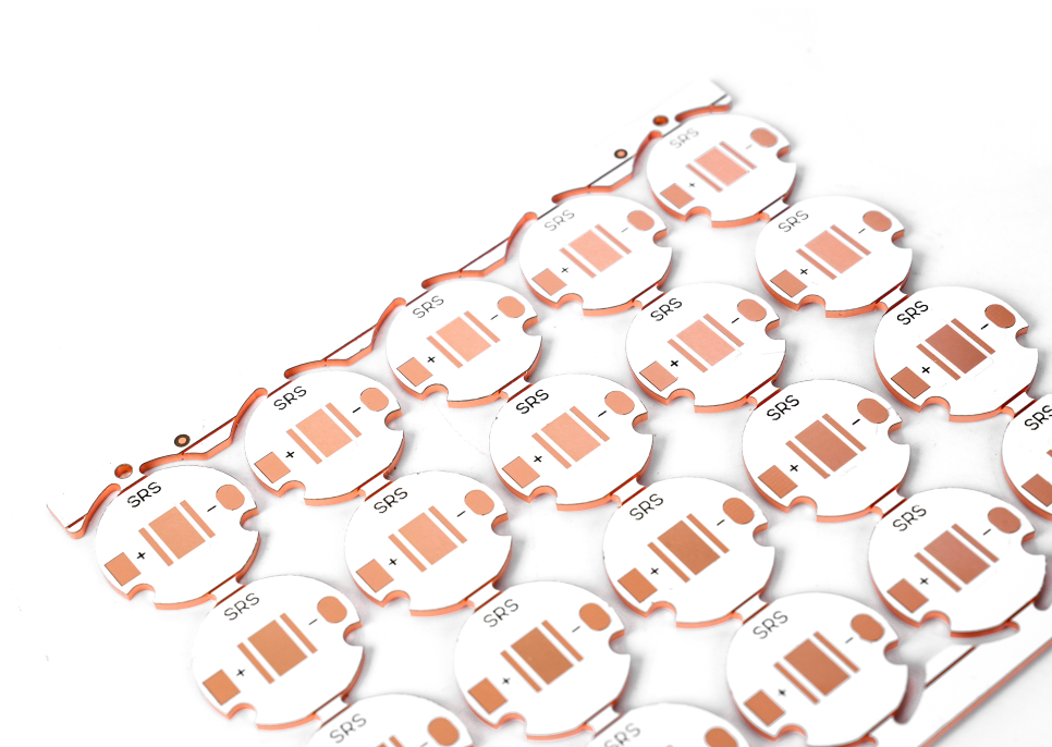
Metal Core (Base Layer)
- Usually aluminum for cost-efficiency and solid heat dissipation.
- Copper is used for high-end applications requiring better conductivity.
Dielectric Layer
- The thin insulation layer offers high thermal conductivity but must resist high voltages.
- Common materials include ceramic-filled polymers.
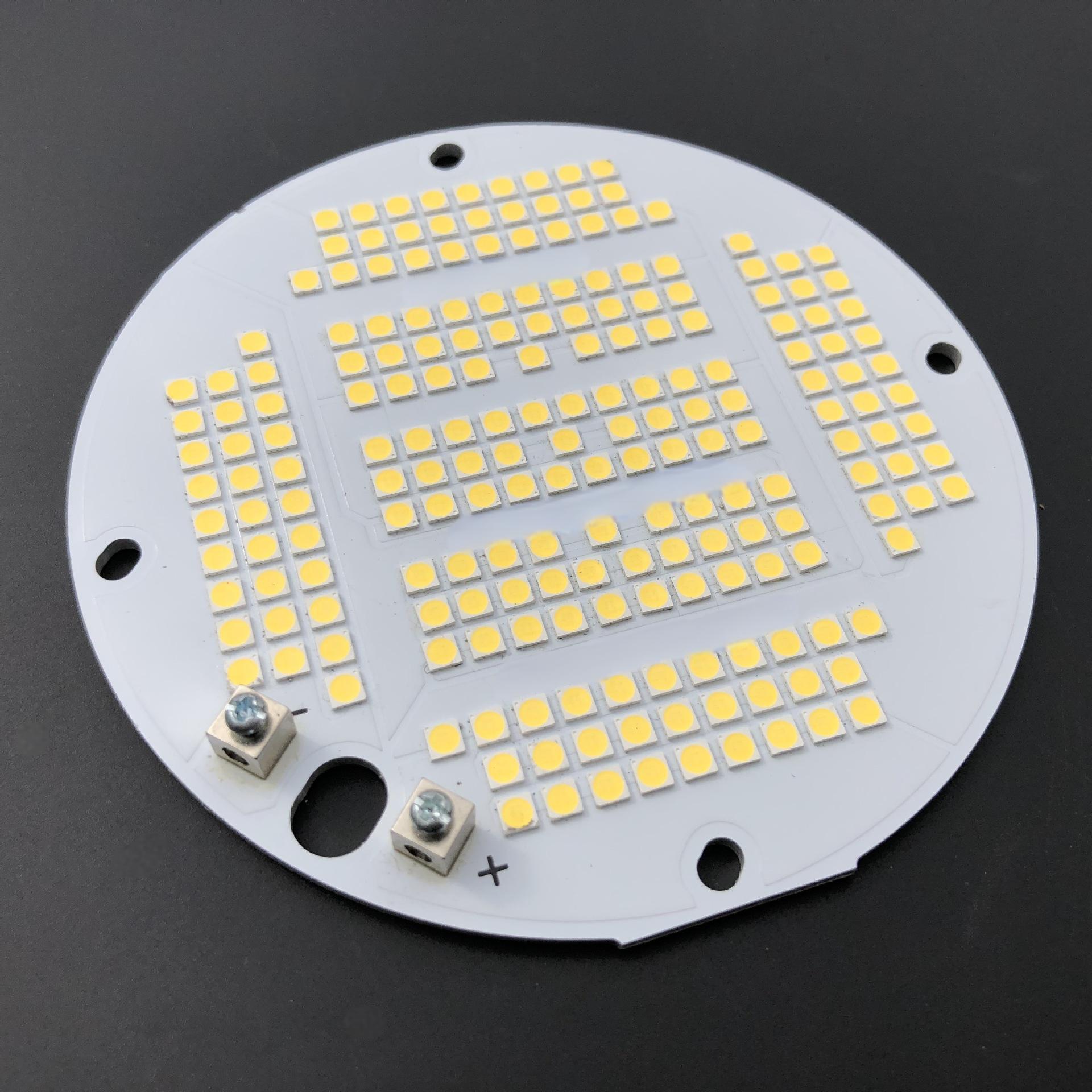
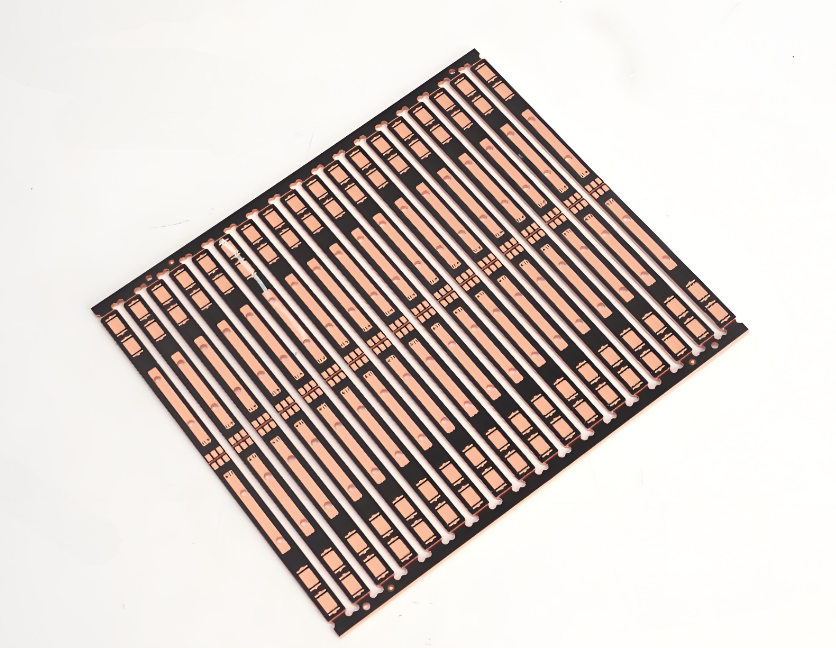
Copper Layer
- Carries the electrical signals and forms circuit traces.
- Thickness varies depending on current-carrying requirements.
Surface Finish
- Prevents oxidation and ensures strong solder connections.
- ENIG, HASL, and OSP are common options.
These materials aren’t just chosen for compatibility. Each plays a role in enhancing performance and lifespan.
What is core in manufacturing process?
In the MCPCB world, the core is the metal base. It plays several roles:
- Heat Dissipation: Pulls heat away from components and spreads it evenly.
- Mechanical Support: Strengthens the board and reduces vibration risks.
- Electrical Isolation: Combined with dielectric materials to ensure circuits don’t short.
Unlike FR4 used in standard boards, a metal core makes MCPCBs suitable for high-wattage devices and LEDs.
How is the chipset protected during MCPCB making?
Chipsets are delicate. During manufacturing, every step must protect their integrity.
- Low Thermal Resistance Layers: These layers keep chipsets cool by drawing heat down quickly.
- Strong Adhesion: Prevents delamination and cracking under stress.
- Stable Solder Pads: Ensures chips stay in place during reflow soldering.
- Controlled Expansion: Metal cores reduce thermal expansion that could otherwise harm chip connections.
These features not only protect but extend the lifespan of integrated circuits.
What sets MCPCB apart from PCB manufacturing?
While the two may look alike, MCPCB and PCB differ in core design and performance:
- Thermal Management: MCPCBs are built for heat. Regular PCBs are not.
- Material Core: FR4 vs. metal (aluminum or copper).
- Applications: MCPCBs are used in LEDs, power supplies, automotive, and RF circuits. Traditional PCBs serve consumer electronics and low-heat applications.
- Durability: MCPCBs hold up better in demanding environments.
In short, if your product generates heat, MCPCBs are the smarter choice.
What is the difference between FR4 and Mcpcb?
FR4 is a fiberglass-reinforced epoxy laminate. It’s lightweight, cheap, and widely used. MCPCB, on the other hand, uses a metal core. Here’s the difference:
Thermal Conductivity:
- FR4: Poor
- MCPCB: Excellent
Structure:
- FR4: All dielectric layers
- MCPCB: Metal core + dielectric + copper
Use Cases:
- FR4: Phones, computers
- MCPCB: LEDs, automotive, industrial devices
Durability:
- MCPCBs are more resistant to mechanical and thermal stress.
How does MCPCB manufacturing improve heat dissipation?
Heat is channeled through the dielectric layer into the metal base. From there, it spreads outward and away from hot spots.
This design drastically reduces the risk of:
- Component burnout
- Solder joint failure
- Signal degradation
MCPCBs also lower the need for additional cooling solutions like heat sinks or fans. This saves space and cost. This makes them ideal for compact or sealed systems like:
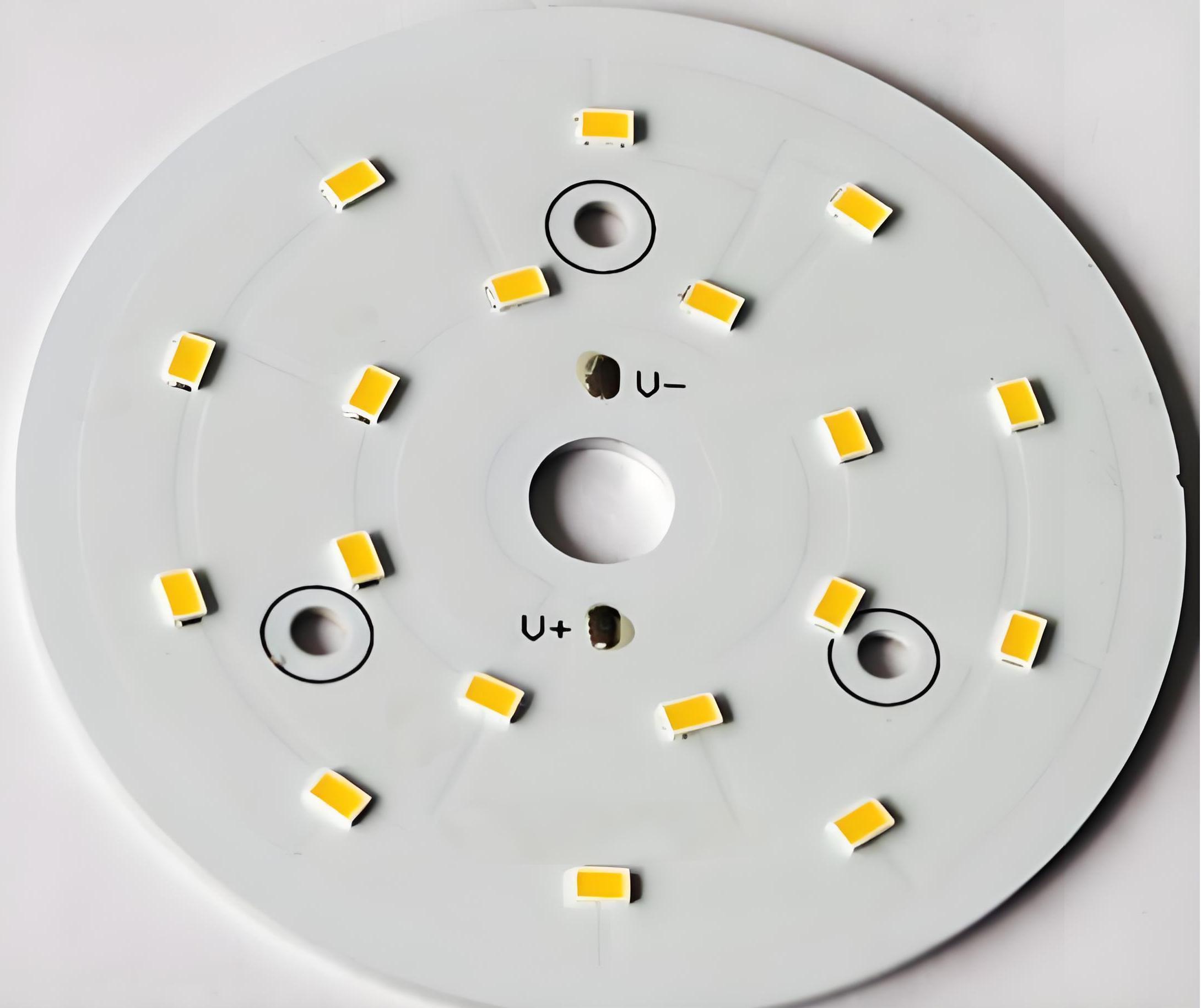
- LED lighting
- Automotive sensors
- Power converters
The key lies in the seamless combination of conductive and insulating materials.
Conclusion:
Understanding the MCPCB manufacturing process will help you understand this product. From chipset protection to thermal performance, it outshines traditional PCBs in demanding applications.
Whether you need reliability, heat control, or performance, MCPCBs are the answer.
Need high-quality MCPCBs with full design and manufacturing support? EBest Circuit (Best Technology) is your trusted partner. Reach out now: Contact us: sales@bestpcbs.com