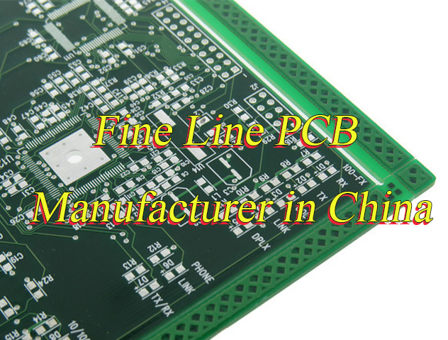
Looking for a PCB manufacturer in Belgium? This blog is mainly about how to choose a reliable Belgium PCB manufacturer and challenges and solutions of Belgium PCB manufacturing companies.
Are you worried about these questions?
- Delivery delays: Project timelines disrupted by production cycle uncertainty, urgent need for predictable delivery timelines.
- Hidden costs: Unexpected additional charges post-project acceptance, requiring transparent cost control mechanisms.
- Quality instability: Batch-to-batch quality variations causing rework risks, demanding reliable quality control standards.
As a 19 year’s PCB manufacturer, EBest Circuit (Best Technology) can provide you service and solutions:
- Delivery predictability: Full production process visibility via ERP+MES dual platforms, guaranteeing 7-day delivery for standard orders and 48-hour response for urgent orders, with ≤2% delay rate and traceable data.
- Cost transparency: Locked total pricing at contract signing using BOM-level cost modeling, covering all processes from material cutting to testing, eliminating post-acceptance add-ons.
- Quality reliability: Triple verification system (AOI inspection + flying probe testing + impedance validation) per IPC-A-600H standards, 100% full inspection for critical processes, defect rate ≤0.3%, batch consistency ≥98%.
Welcome to contact us if you have any request for PCB and PCBA service: sales@bestpcbs.com.
Top 10 PCB Manufacturer in Belgium
1. Citec Group
- Main Business: Standard FR-4 PCB manufacturing, fast prototype runs, industrial PCB supply.
- Advantages: Responsive engineering help, stable delivery for small development batches, easy communication for European clients.
- Production Capabilities: 1–8 layer FR-4 PCBs; Standard copper thickness; Solder mask, silkscreen, and basic surface finishes; Electrical testing for most designs.
- Typical Lead Time: 5–7 working days for prototypes; 10–15 working days for small series.
2. Eurocircuits
- Main Business: Online PCB fabrication and PCB assembly for prototypes and small series.
- Advantages: Instant online pricing, very strong data checking system, transparent manufacturing routes, and stable EU-based processes.
- Production Capabilities: 2–10 layer FR-4 boards; Controlled impedance for standard designs; Stencils, assembly, and DFM tools; Mixed-technology SMT/THT assembly.
- Typical Lead Time: As fast as 3 working days for bare board prototypes; 6 working days for standard PCB + assembly service.
3. Acelio Electronics
- Main Business: PCB manufacturing and EMS services for automation, medical, and industrial electronics.
- Advantages: Broad support for product design cycles, stable documentation handling, and tight quality control.
- Production Capabilities: Rigid PCBs for sensors, automation boards, medical devices; Multilayer boards for industrial control; SMT and THT assembly for small and medium runs.
- Typical Lead Time: 7–10 working days for prototypes; 15–25 working days for mass production. The specifics depend on the complexity of the project.
4. Interstate Europe
- Main Business: PCB production services for various industries, from telecom to industrial machines.
- Advantages: Reliable quality records and broad material availability for common FR-4 needs.
- Production Capabilities: Rigid boards for general electronic products; Multi-layer fabrication with standard tolerances; Surface finishing options for mainstream applications.
- Typical Lead Time: 10–15 working days for standard production; Complex constructions are typically priced per project.
5. CIM Electronics Belgium
- Main Business: Electronics manufacturing, high-mix assembly, and PCB-related services.
- Advantages: Strong assembly know-how, good at handling many part numbers, and reliable in low-to-medium volume production.
- Production Capabilities: SMT and THT assembly; Mixed-technology builds; Box build and sub-assemblies; Functional testing on request.
- Typical Lead Time: Assembly prototypes: 7–12 working days for assembly prototypes; 20–30 working days for production batches; CIM Electronics works well with companies who need full EMS support rather than just bare boards.
6. ATS Electronics
- Main Business: PCB assembly, electronics integration, and module production.
- Advantages: Ability to handle complex assemblies, strong documentation support, and flexible production lines.
- Production Capabilities: SMT, THT, and wave soldering; Hybrid builds for sensors and industrial controls. System integration and testing.
- Typical Lead Time: 8–12 working days for prototype assembly; 20–25 working days for medium volume production.
7. IPTE Factory Automation
- Main Business: Automation systems plus PCB-related services, including test fixtures and production equipment.
- Advantages: Deep automation expertise, ideal for customers who need production test solutions and equipment near their PCB supplier.
- Production Capabilities: In-circuit test stations; Functional test systems; Automated machines for PCB processes; Some small-scale PCB-related services.
- Typical Lead Time: PCB service tasks: usually within 10–20 working days;
8. DVC NV
- Main Business: Full EMS service, from ideation and design to PCB plate-making, assembly, testing, and after-sales.
- Advantages: One-stop technical collaboration, strong application-specific development experience, and long-term product support.
- Production Capabilities: Rigid and rigid-flex options; PCB assembly for industrial, telecom, and heating equipment; In-house testing procedures and upgrades.
- Typical Lead Time: 7–10 working days for prototypes; 20–30 working days for mass production.
9. Meerssen Electronics
- Main Business: Custom industrial electronics and PCB manufacturing for control modules.
- Advantages: Strong in producing tailor-made solutions, helpful for OEMs in machinery, power systems, and automation.
- Production Capabilities: Low-to-medium volume PCB builds; Customized electronics modules; Assembly and testing for specific industrial needs.
- Typical Lead Time: 10–12 working days for development boards; 20–25 working days for mass production .
10. BCM Electronics Europe
- Main Business: Specialized PCB builds for telecom, industrial monitoring, and communication devices.
- Advantages: Experienced in telecom-grade reliability, consistent electrical performance, and stable project continuity.
- Production Capabilities: Multilayer rigid boards; Telecom circuit assembly; Reliability-focused testing processes.
- Typical Lead Time: 7–10 working days for prototypes; 15–25 working days for medium bulk production.
How to Choose A Reliable PCB Manufacturer in Belgium?
A Detailed Selection Guide to Belgium PCB Manufacturing Company:
1. Match Professional Domain
- Prioritize visiting the “Technical Capabilities” or “Product Catalog” sections of the target vendor’s official website, and filter for vendors that clearly indicate specific areas such as “Prototype Making,” “High-Density Interconnect (HDI),” and “Flexible Circuits.”
- Query the Belgian Electronics Industry Association (e.g., Agoria) website for registered member lists to identify local manufacturers specializing in target application domains (e.g., medical devices, automotive electronics, industrial controls).
- Attend Belgian electronics trade shows (e.g., SMTconnect Brussels) to directly engage with manufacturer technical teams and verify professional domain alignment.
2. Verify Quality Certifications
- Request scanned copies of manufacturer certifications and cross-check certificate numbers with issuing authority records (e.g., verify ISO 9001 certificate validity via the ISO website).
- For automotive, medical, or other specialized industries, confirm whether the manufacturer holds dedicated certifications such as IATF 16949 or ISO 13485, and verify the process scope covered by these certificates (e.g., soldering, coating, testing).
- Validate whether the manufacturer has passed third-party safety certifications such as UL or TÜV to ensure products meet EU CE directives and RoHS environmental standards.
3. Evaluate Technical Capabilities
- Request a detailed process parameter sheet from the manufacturer, including maximum layer count, minimum trace width/spacing, minimum hole size, substrate types (e.g., high-frequency FR4, polyimide flexible substrates), and surface finish processes (e.g., ENIG, OSP).
- Obtain lists of production equipment and inspection equipment, focusing on confirming models, precision, and maintenance records for key devices such as laser drilling machines, AOI automatic optical inspection systems, and flying probe testers.
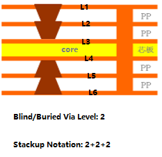
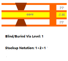
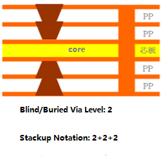
- Verify the manufacturer’s support for specialized processes (e.g., blind/buried vias, backdrilling, metal-core substrate thermal design) through technical Q&A.
4. Utilize Design Support Tools
- Preferentially use the manufacturer’s online DFM (Design for Manufacturability) tools to upload Gerber files and receive real-time feedback on trace width/spacing violations, drilling dimension deviations, pad design defects, etc., avoiding post-production modification costs.
- If the manufacturer lacks online tools, request a DFM check report template and clarify the specific inspection items included (e.g., impedance control, thermal design, testability design).
- For complex designs, request free design consultation services to optimize layouts and reduce manufacturing costs.
5. Clarify Delivery and Supply Chain
- Request a standard lead time table from the manufacturer, distinguishing between prototype (typically 5-10 days), small batch (2-3 weeks), and large batch (4-6 weeks) lead times, and clarify conditions and costs for expedited services.
- Review the manufacturer’s supply chain management strategy, including inventory levels for critical raw materials (e.g., copper foil, resin), supplier qualifications (e.g., ISO certification), logistics partners (e.g., DHL, FedEx), and transit times.
- For urgent needs, confirm whether the manufacturer offers local warehousing or rapid response services (e.g., 24-hour emergency production).
6. Obtain Reference Cases
- Request success cases from the manufacturer that are highly relevant to the target industry, including project names, application scenarios, technical challenges, and end-customer evaluations.
- Contact clients from the referenced cases via LinkedIn or industry associations to verify case authenticity and manufacturer performance (e.g., quality stability, on-time delivery rate, post-sales support).
- Prioritize cases involving Belgian local enterprises to validate adaptability in the European market.
7. Compare Detailed Quotes
- Request itemized quotation sheets from manufacturers, specifying material costs, processing fees, surface finish costs, testing fees, packaging fees, taxes, and potential additional charges (e.g., engineering fees, mold fees).
- Compare quotation transparency across multiple manufacturers, prioritizing those providing detailed cost breakdowns (e.g., per-layer pricing, per-square-meter material costs) to avoid hidden costs (e.g., rework fees, rush fees).
- For large-volume orders, request tiered pricing or long-term partnership discount schemes.
8. Conduct On-Site or Virtual Factory Audits
- When scheduling virtual factory audits, request the manufacturer to showcase the full production workflow (from material cutting to final testing), focusing on cleanroom class (e.g., ISO Class 7), equipment maintenance records, and employee operational standards (e.g., ESD precautions).
- During on-site inspections, pay attention to calibration certificates and usage records for inspection equipment (e.g., flying probe testers, X-ray inspection systems) to verify actual testing capabilities.
- For critical projects, commission third-party inspection agencies (e.g., SGS, DEKRA) for on-site audits to ensure the manufacturer’s process standards meet requirements.
Challenges Faced by PCB Manufacturer in Belgium
Unique Cost Burdens of the Local Market
- High Local and Neighboring Country Prices: The scarcity and high prices of local PCB manufacturers often result in Belgian customers incurring costs 30-40% higher than international suppliers.
- Complex VAT and Customs Procedures: The 21% Belgian VAT on imported PCBs is strictly enforced, and customs may reclassify goods, leading to additional taxes, fees, and logistical delays. Local quotes typically do not include taxes, easily causing budget overruns.
Compliance and Quality Risks in the EU Core Area
- Strict EU Regulatory Review: As an EU hub, Belgian companies face more stringent audits of regulations such as RoHS and REACH. Non-compliance can result in significant business losses.
- Quality Discrepancies from “EU Sourcing”: When selecting suppliers from the EU, such as Germany and France, the actual delivered PCBs may have quality issues such as misaligned drill holes and solder mask peeling, failing to meet the expected “EU quality.”
Bilingualism and Cross-Border Communication Barriers
- Insufficient Language Support: The bilingual (Dutch and French) environment in Belgium makes it easy for customers to misunderstand when communicating with suppliers lacking adequate bilingual support, potentially leading to production errors.
- Slow Response from EU Suppliers: Suppliers from EU countries such as Germany may take more than 48 hours to respond to inquiries in languages like Dutch. Local supplier customer service responses are also slow, impacting project schedules.
Supply Chain Vulnerability and Logistics Delays
- Port Congestion and Transit Risks: Reliance on the Port of Antwerp makes PCB transportation susceptible to delays due to factors such as port strikes. Following Brexit, trucks entering from Germany also face longer border checks.
- Limited Local Rapid Prototyping Capabilities: Local suppliers provide long lead times for prototype PCBs (e.g., 10 days), which cannot meet urgent needs, forcing customers to turn to overseas suppliers with faster delivery times.
Our PCB Solutions for These Challenges
This is the solution we can offer to address the aforementioned difficulties and challenges:
1. Competitive Transparent Costs, Eliminating Budget Risks
- Significant Price Advantage: Leveraging scaled production and efficient supply chains, we deliver core material costs at least 30% lower than Belgian local and neighboring European suppliers.
- All-Inclusive Pricing & Tax Support: Clear quotes include DDP (Delivered Duty Paid) options, covering all fees upfront. Our logistics partners, familiar with Belgian customs procedures, assist with 21% VAT handling and customs clearance to ensure no hidden costs or unexpected delays.
2. EU Compliance Guarantee & Consistent Quality
- Comprehensive Compliance Documentation: All products strictly adhere to EU core regulations including RoHS (2011/65/EU) and REACH, with compliant declarations and test reports (if required) provided alongside shipments to facilitate audits in Belgium and the EU.
- Data-Driven Quality Assurance: Full automation in production processes and multi-layer optical inspections (AOI/AXI) ensure reliability across drilling precision, solder mask adhesion, and other critical steps. We willingly share key process quality control data to replace vague trust in “EU quality” with factual evidence.
3. Professional Localized Communication & Seamless Collaboration
- Bilingual Technical Support: Dedicated technical customer service and engineering teams fluent in English and French accurately interpret professional requirements like “operating frequency,” ensuring zero miscommunication in technical documents and preventing production errors caused by language barriers.
- Rapid Response Service Model: Timely support during your working hours (typically within hours) via a dedicated account manager eliminates delays, resolving project extension risks tied to communication lags.
4. Robust Supply Chain & Agile Logistics
- Optimized Logistics Routes & Tracking: Multiple stable European shipping routes avoid single-port dependency. Real-time logistics tracking and proactive alerts for anomalies (e.g., port congestion) keep you informed of shipment status.
- Quick Prototyping & Flexible Delivery: Standard 5-7 day prototyping outperforms local European suppliers, while small-batch flexibility and optional European buffer stock solutions drastically reduce R&D and market response times.
Why Belgium Clients Choose EBest Circuit (Best Technology) for PCB Manufacturer?
Reasons Why Belgium Clients Choose EBest Circuit (Best Technology) as PCB Manufacturer:
- Clear Pricing with No Hidden Costs: We provide straightforward, easy-to-understand pricing where every cost is visible upfront. Customers never face unexpected charges after project completion—what you see is what you pay, ensuring full budget control from start to finish.
- Cost-Sensitive Design Optimization: Leveraging 19 years of industry expertise, we analyze material choices and process improvements to deliver measurable cost savings, typically 15–30% lower manufacturing expenses without compromising quality.
- 24-Hour Rapid Prototyping for Urgent Orders: Our dedicated fast-track production line delivers sample prototypes within 24 hours, meeting critical needs for industries like medical devices and automotive electronics where speed is essential.
- 99.2% On-Time Delivery Rate: Through intelligent production scheduling and global logistics coordination, we achieve an industry-leading on-time delivery rate. Less than 1% of orders experience minor delays, outperforming sector averages significantly.
- Quality Control with Multiple Certifications: Every batch undergoes 100% inspection, backed by ISO 19001, IATF 16949 automotive standards, medical-grade RoHS compliance, and IATAF aviation certifications, ensuring compliance with the highest regulatory requirements across sectors.
- Data-Driven Process Improvement: Our 19-year production error database identifies recurring issues and proactively adjusts processes, boosting first-pass yields by over 20% and reducing client rework costs.
- Free DFM (Design for Manufacturing) Analysis: We offer complimentary evaluations to spot design flaws early, streamline manufacturability, and cut development time by up to 30%, saving both time and money.
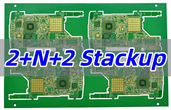
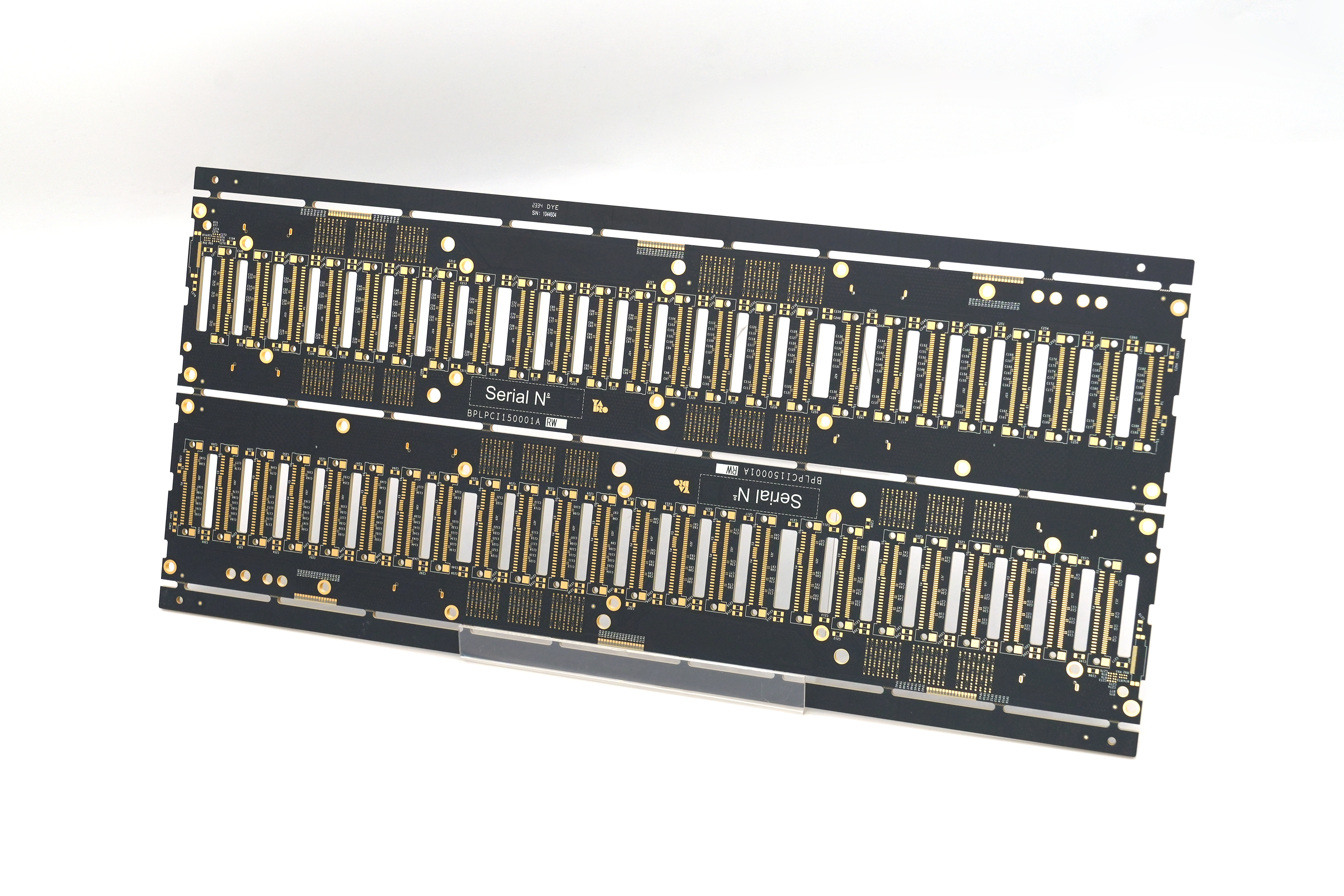
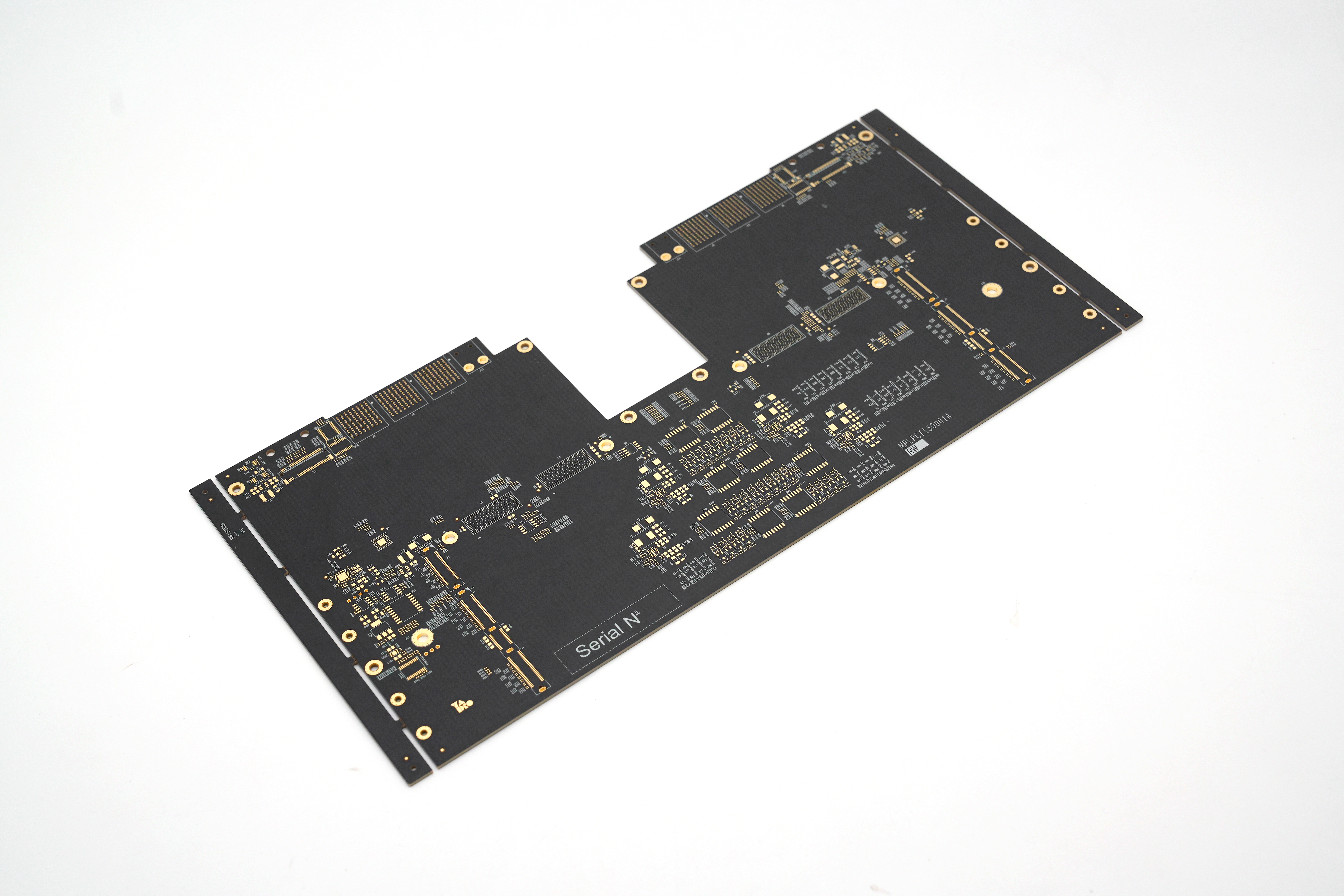
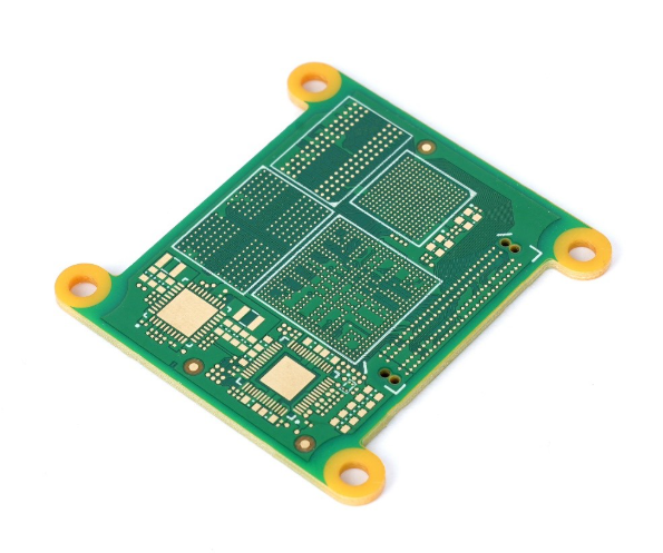
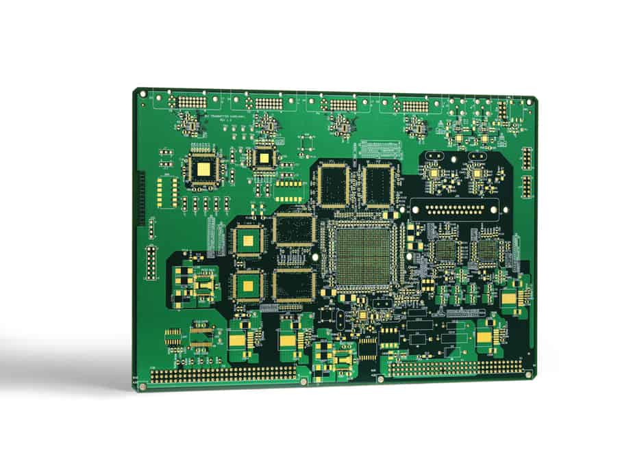
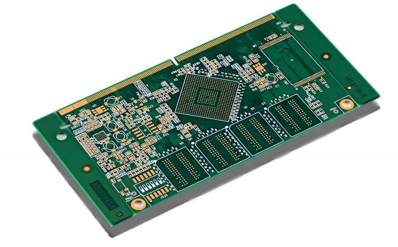
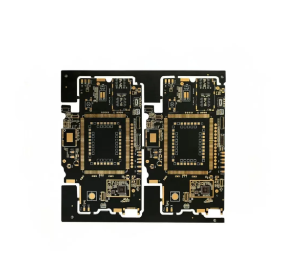
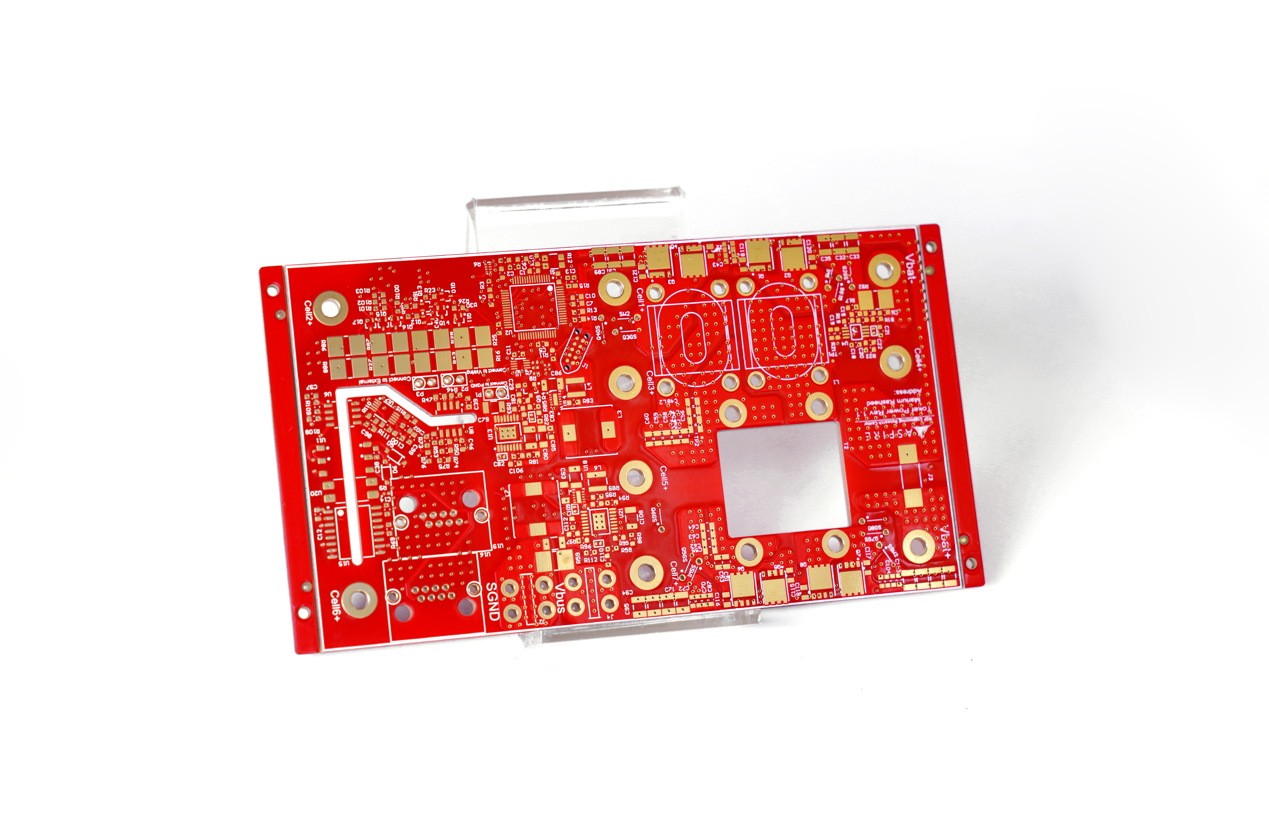
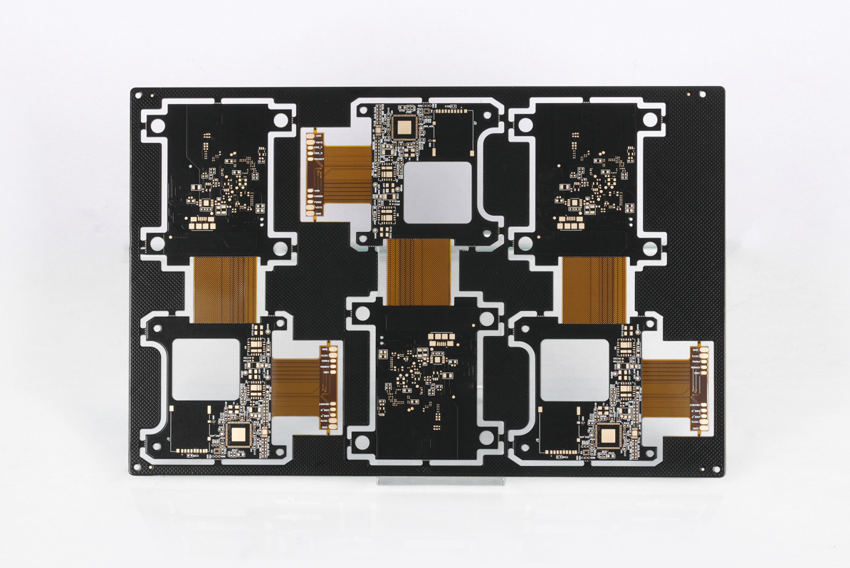
Attached is a photo of rigid-flex circuits for your reference:
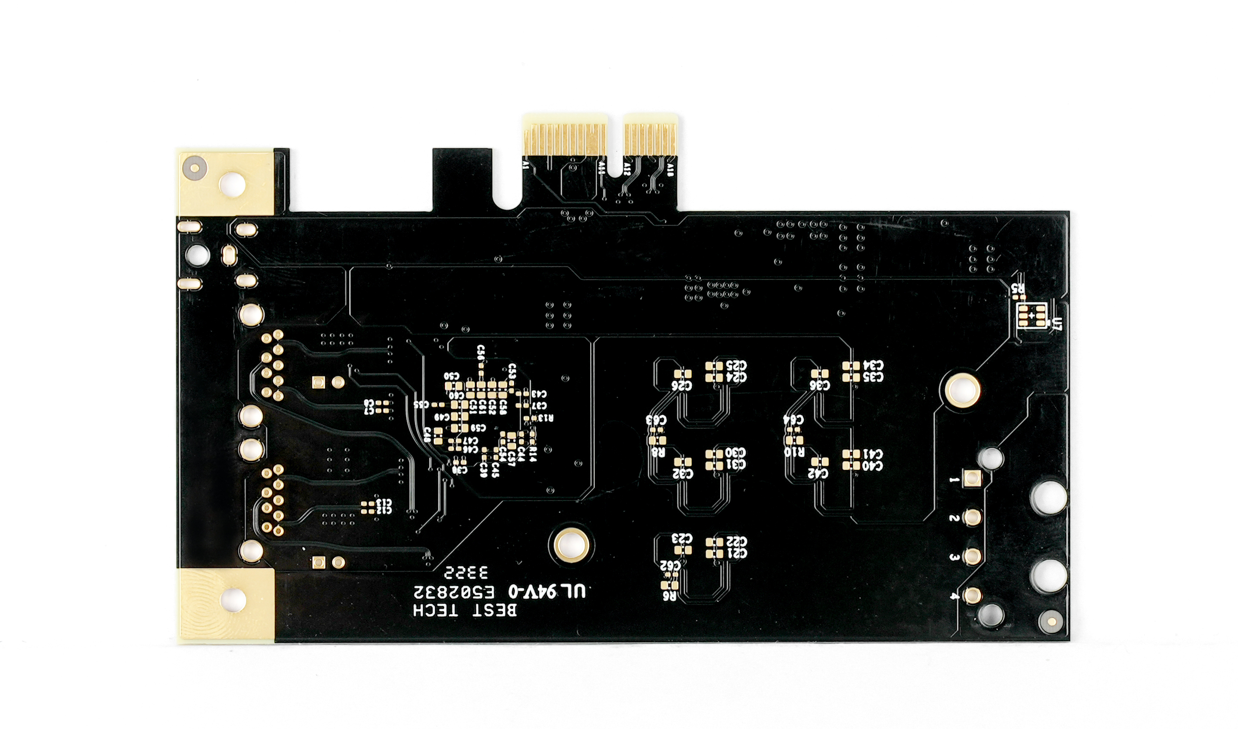
Types of PCB We Can Offer You
- FR4 PCB( Single Layer PCB, 2 Layers PCB, Multi-layer PCB)
- MCPCB(Single Layer MCPCB, 2 Layers MCPCB)
- FPC( Single Sided Flexible Circuits, Double Sided Flexible Circuits, Multilayer Flexible Circuits, Dual Access Flexible Circuits, Rigid-Flex Circuits)
- Ceramic PCB( Thick Film Ceramic PCB, Thin Film Ceramic PCB, DCB Ceramic PCB)
- Heavy Copper PCB
- Bus Bar PCB
- Extra Thin PCB
- High Tg PCB
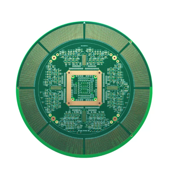
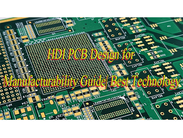
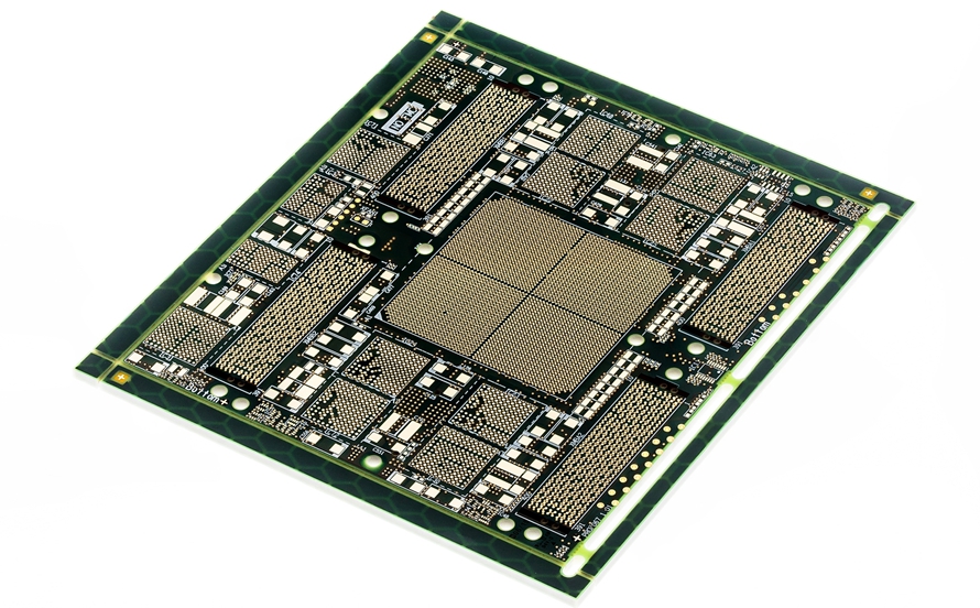
- HDI PCB
- RF Board
Our Quality Certifications of PCB Manufacturing
- ISO9001:2015
- ISO13485:2016
- REACH
- RoHS
- UL
- IATF16949
- AS9100D
Case Studies of Our Belgium PCB Manufacturing
Project Background
- A medium-sized manufacturer specializing in industrial automation equipment in Belgium requires highly reliable multi-layer printed circuit boards (PCBs) for its core products. Due to product iterations, its original PCB supplier faced issues in product quality stability and on-time delivery rate, causing multiple production line shutdowns from PCB defects and severely impacting delivery commitments to end customers.
Customer Requirements
- Quality and Reliability: PCBs must meet IPC-A-600 Class 3 standards to ensure stable long-term operation in harsh industrial environments.
- Process Complexity: Production of 10-layer High-Density Interconnect (HDI) boards involving precision processes like laser blind vias.
- Sustainability: Focus on environmental performance in production, specifically optimizing water resource utilization and reducing wastewater discharge.
- Supply Chain Resilience: Suppliers need stable production capacity and rapid response capabilities to handle order fluctuations.
Customized Solutions
- Technical Process Optimization: Adopted Laser-Assisted Seeding (LAS) Microvia Plating Technology for HDI boards, enhancing uniformity and reliability of copper layers on high-aspect-ratio microvias while improving thermal performance versus traditional processes.
- Intelligent Water Management System: Implemented real-time monitoring and cyclic optimization for water used in wet processes (cleaning, electroplating) during PCB production, significantly reducing freshwater consumption and wastewater discharge.
- Flexible Production and Delivery: Reserved dedicated capacity for the customer and established a weekly synchronized delivery tracking mechanism to ensure order priority.
Results
- Quality Improvement: PCB delivery yield stabilized above 99.5%, eliminating production line shutdowns from PCB issues.
- Efficiency and Cost: Unit product water consumption reduced by approximately 18% via the Intelligent Water Management System, with associated reductions in water treatment costs.
- Delivery Performance: Achieved 100% on-time delivery rate for orders, fully meeting the customer’s production rhythm needs.
- Technical Compliance: 10-layer HDI boards passed all customer reliability tests, including high-temperature/high-humidity and vibration tests.
How to Get a Quote for Your Printed Circuit Board Project?
Streamlined Process for Obtaining PCB Project Quotes:
1. Clarify Project Requirement Details
- Confirm PCB type (e.g., single-layer, double-layer, multi-layer), layer count, dimensions, materials (e.g., FR4, aluminum substrate), surface finishes (e.g., HASL, ENIG, OSP), solder mask color, and process parameters like minimum trace width/spacing.
- Specify special processes (e.g., blind/buried vias, impedance control, high-frequency materials), testing requirements (e.g., flying probe test, ICT), and quality certification standards (e.g., IPC-A-600, RoHS, UL).
2. Prepare Essential Materials for Streamlined Quotation
- Gerber Files: Standard format files (generated by EDA tools like Altium, OrCAD) containing PCB layout, drilling, solder mask layer data.
- BOM List: Bill of materials detailing component models, brands, quantities, and alternative part information.
- Process Specification Documents: Including special process requirements, tolerance standards, and test protocols.
- Quantity & Lead Time Requirements: Define order quantities (e.g., prototypes, small batch, mass production) and desired delivery timelines.
- Contact Information & Drawings: Provide project contact, company name, address, and assembly drawings (if applicable).
3. Select International Suppliers & Communicate
- Filter manufacturers with export qualifications via supplier websites, industry exhibitions, or platforms (e.g., Alibaba, PCBWay), prioritizing English-speaking suppliers with Euro-American market experience.
- When submitting files, ensure compatibility (e.g., Gerber 274X, ODB++) and avoid Chinese-named files; include English technical specifications.
4. Obtain & Compare Quotes
- Suppliers typically provide preliminary quotes within 24–48 hours, covering unit price, MOQ, lead time, and payment terms (e.g., T/T, PayPal).
- For international clients, request detailed quotes including material costs, processing fees, testing fees, packaging/shipping costs (e.g., FOB, CIF), and tariff notes.
5. Confirm Collaboration & Follow-Up
- Before contract signing, verify supplier support for international shipping (e.g., DHL, FedEx), payment currencies (e.g., USD, EUR), and after-sales services (e.g., warranty, return policies).
- Post-order placement, maintain communication to track production progress and ensure compliance with delivery timelines and quality standards.
Welcome to contact us if you have any request for PCB design, prototyping, mass production and assembly project: sales@bestpcbs.com.