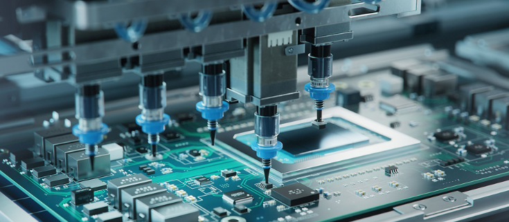
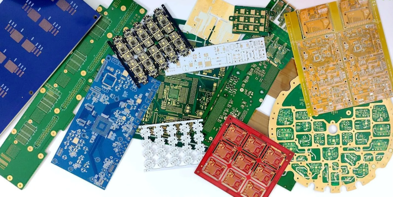
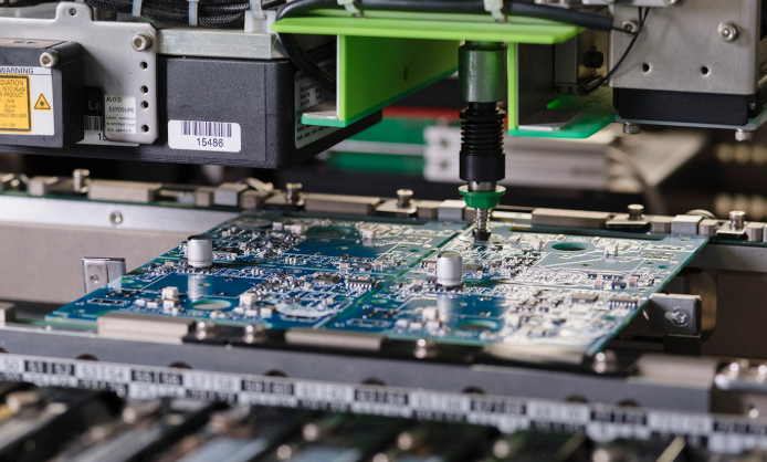
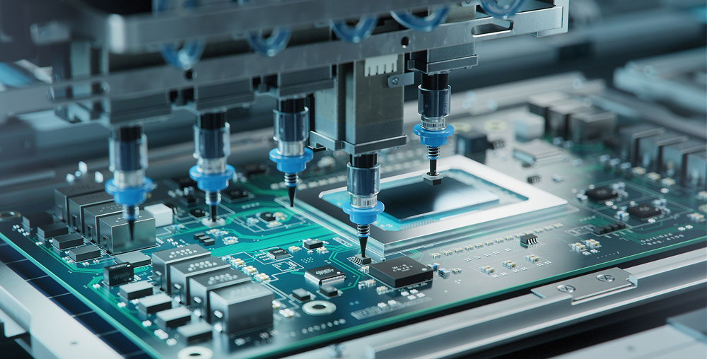
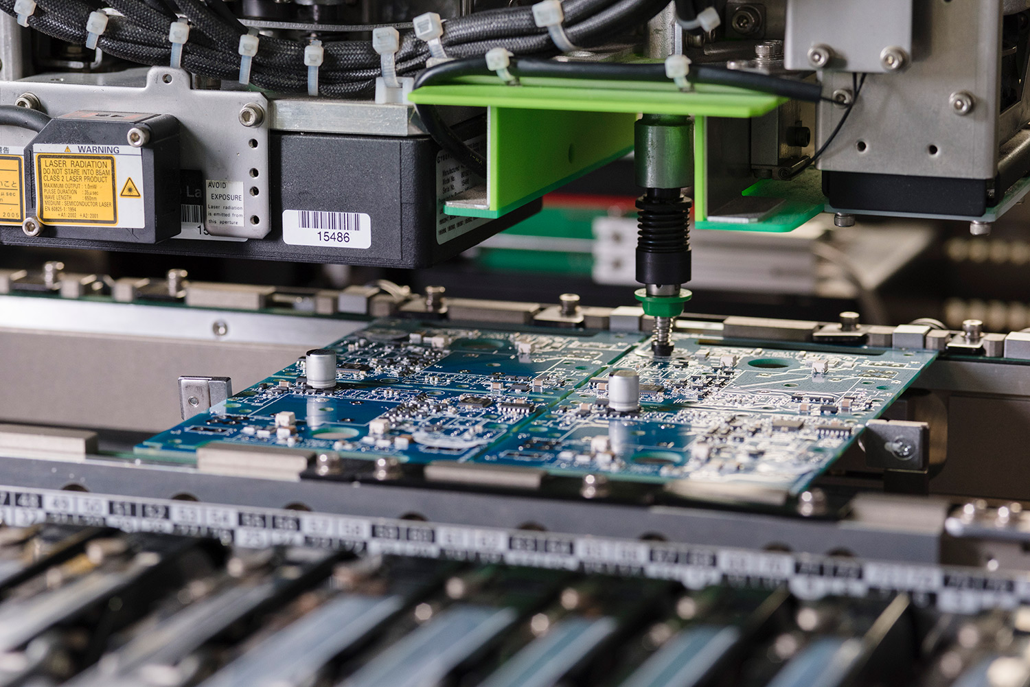
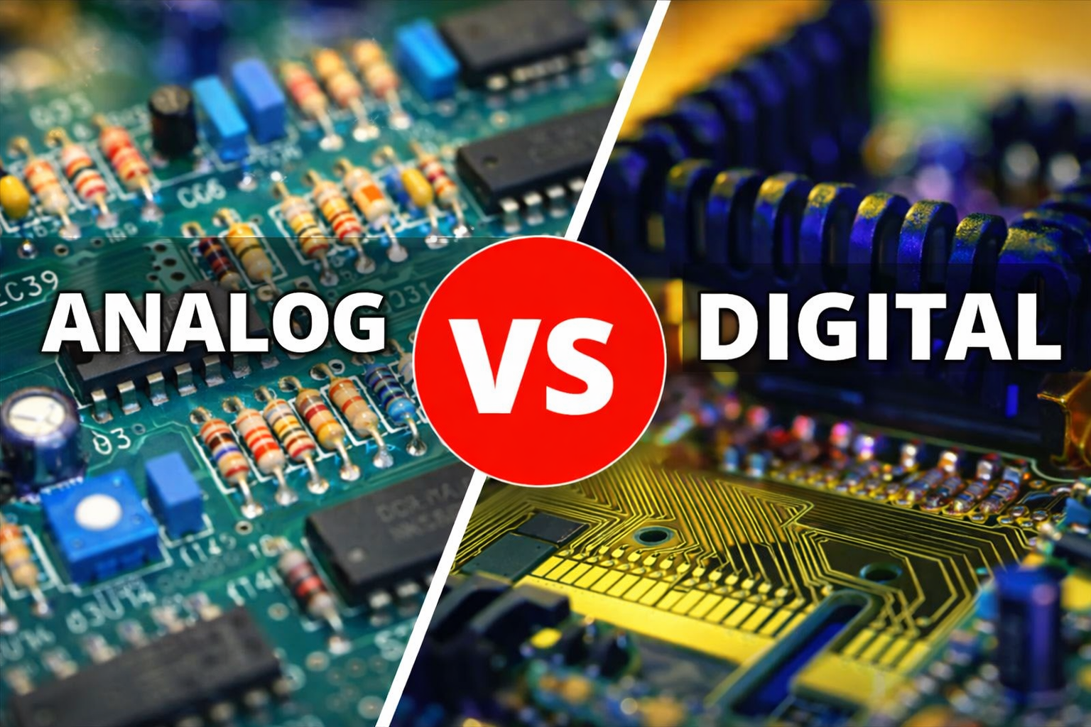
Understanding analog circuit vs digital circuit fundamentals is essential in modern electronics, especially as products increasingly combine both domains on the same printed circuit board. While the terms are often used interchangeably in casual discussions, analog and digital circuits differ fundamentally in how they process signals, how they are designed, and where they are best applied.
This guide explains analog and digital circuits from a practical engineering perspective, using real examples and clear comparisons to help you make the right design decisions.
What Is an Analog Circuit?
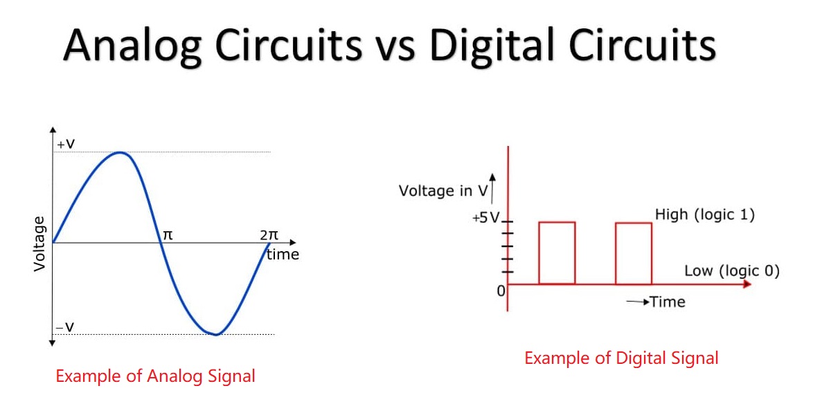
An analog circuit processes continuous signals. Voltage or current varies smoothly over time, directly representing real-world physical quantities such as sound, temperature, pressure, or light intensity.
In an analog circuit, small changes at the input create proportional changes at the output. There are no discrete steps or fixed logic states. This continuous behavior allows analog circuits to preserve subtle signal details.
Typical characteristics of analog circuits include:
- Continuously varying voltage or current
- Sensitivity to noise and interference
- Direct interaction with real-world signals
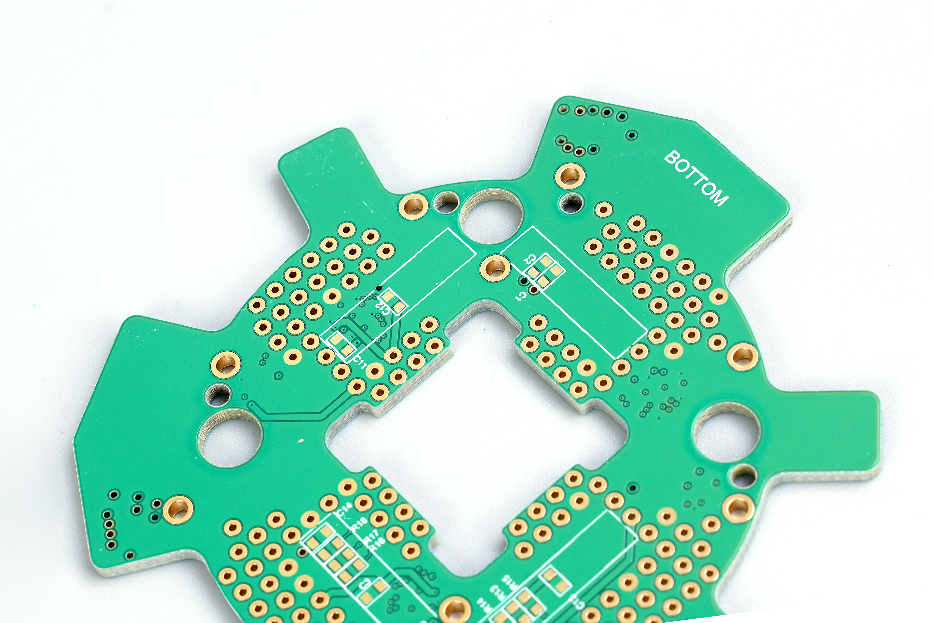
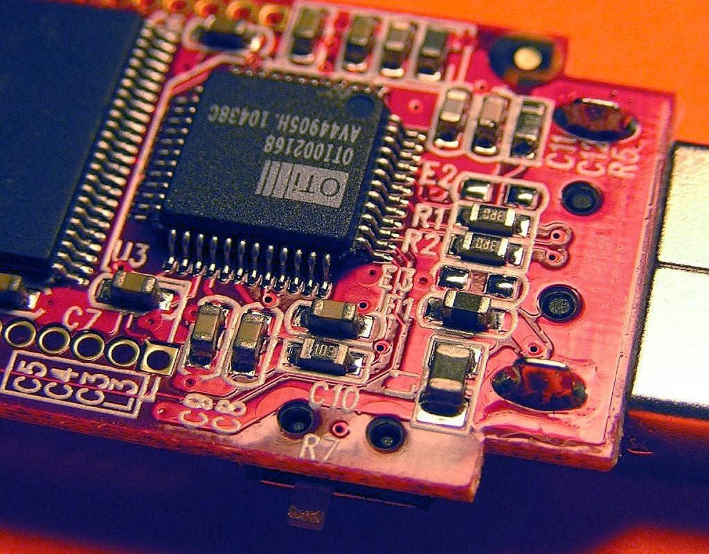
Common components found in analog circuits include resistors, capacitors, inductors, operational amplifiers, and transistors operating in their linear regions.
Analog Circuit Diagram
An analog circuit diagram usually shows smooth signal paths and linear amplification stages. The schematic emphasizes component values, biasing networks, and signal integrity.
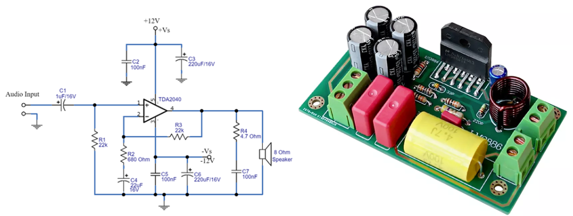
Examples include audio amplifiers, sensor conditioning circuits, and voltage regulators, where signal accuracy is more important than discrete logic states.
What Is a Digital Circuit?
A digital circuit processes discrete signals, typically represented as binary values: logic “0” and logic “1”. These values correspond to defined voltage thresholds rather than continuous variations.
Digital circuits operate on the principle of decision making. Instead of preserving every nuance of a signal, they determine whether the input is above or below a threshold.
Key characteristics of digital circuits include:
- Discrete logic levels
- Strong noise immunity
- Predictable and repeatable behavior
Digital circuits rely on logic gates, flip-flops, microcontrollers, memory devices, and processors.
Digital Circuit Diagram
A digital circuit diagram focuses on logic relationships rather than continuous waveforms. Schematics highlight logic gates, clock signals, data buses, and power integrity.
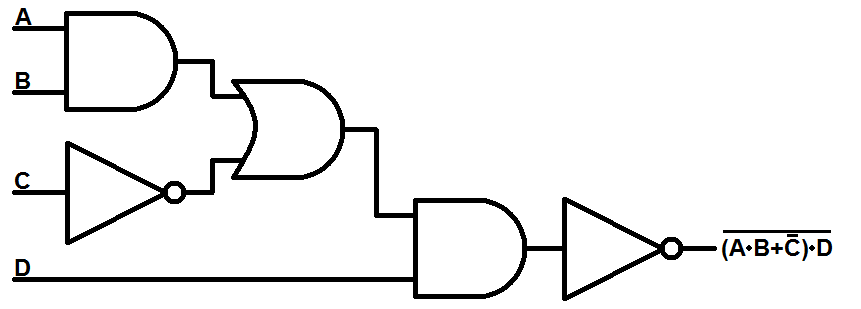
Digital designs prioritize timing, synchronization, and reliable logic transitions rather than exact voltage values.
Analog and Digital Circuits Examples
Analog circuits work with continuous signals, where voltage or current changes smoothly over time, similar to a dimmer switch. These circuits directly process real-world physical signals and are typically built using components such as operational amplifiers, resistors, capacitors, and inductors. Analog circuit examples:
- Audio amplifiers
- Microphone preamplifiers
- Temperature and pressure sensor interfaces
- RF front-end circuits
Digital circuits operate using discrete binary signals, represented as logic 0 and logic 1. They process data through defined logic states and require analog-to-digital (ADC) and digital-to-analog (DAC) conversion when interacting with real-world signals. Digital circuit examples:
- Microcontroller systems
- Computers and smartphones
- Digital clocks and counters
- Communication processors
In many real products, analog and digital circuits coexist. A sensor may produce an analog signal, which is then converted into digital data for processing.
What Is the Difference Between Analog and Digital Circuits?
The core difference between analog and digital circuits lies in signal representation. Analog circuits represent information using continuously varying electrical quantities. Digital circuits represent information using discrete logic states.
Other practical differences include:
- Analog circuits emphasize signal fidelity
- Digital circuits emphasize robustness and repeatability
- Analog performance depends heavily on component tolerances
- Digital performance depends on timing and logic thresholds
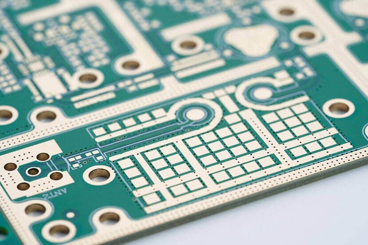
Understanding these differences helps avoid common design mistakes, especially in mixed-signal PCB layouts.
Analog Circuit vs Digital Circuit Pros and Cons
Analog circuit advantages:
- High signal resolution
- Natural interface with physical sensors
- Low latency signal response
Analog circuit limitations:
- Susceptible to noise
- Harder to scale and reproduce consistently
- Component drift over temperature and time
Digital circuit advantages:
- Strong noise immunity
- Easy data storage and processing
- Scalable and programmable
Digital circuit limitations:
- Requires conversion from analog sources
- Quantization errors
- Clock and timing constraints
Neither approach is universally superior. The best choice depends on the application.
How to Tell If a Circuit Is Analog or Digital?
You can usually identify a circuit type by observing:
- Signal behavior on an oscilloscope
- Component types used
- Presence of clock signals
If voltage changes smoothly and continuously, the circuit is analog. If voltage jumps between defined levels, the circuit is digital.
Schematics also provide clues. Analog circuits show amplifiers and filters, digital circuits show logic symbols and data paths.
How Do I Know If My TV Is Analog or Digital?
Modern televisions are digital devices. They process digital video signals internally, even if they accept analog inputs.
If a TV supports HDMI, digital broadcasting standards, or internal digital signal processing, it operates digitally. Older CRT televisions relied more heavily on analog signal paths.
Most consumer electronics today convert any analog input into digital form for processing.
Why Is Digital Better Than Analog?
Digital is often considered better because it offers:
- Better noise resistance
- Easier data compression and storage
- Consistent signal quality over distance
However, digital systems still rely on analog circuits at their inputs and outputs. Power regulation, signal sensing, and RF reception remain analog challenges. Digital is not a replacement for analog, it is a complement.
When Would You Use Analog vs Digital in Circuits?
Use analog circuits when:
- Interfacing directly with sensors
- Preserving signal detail is critical
- Latency must be minimal
Use digital circuits when:
- Data processing and storage are required
- System complexity is high
- Noise immunity is essential
Most modern systems are mixed-signal designs. The analog section captures real-world signals, while the digital section processes and controls them.
Understanding analog circuit vs digital circuit behavior is the foundation of reliable electronic design, especially in applications such as medical devices, industrial control, and communication systems where accuracy and stability are equally important.