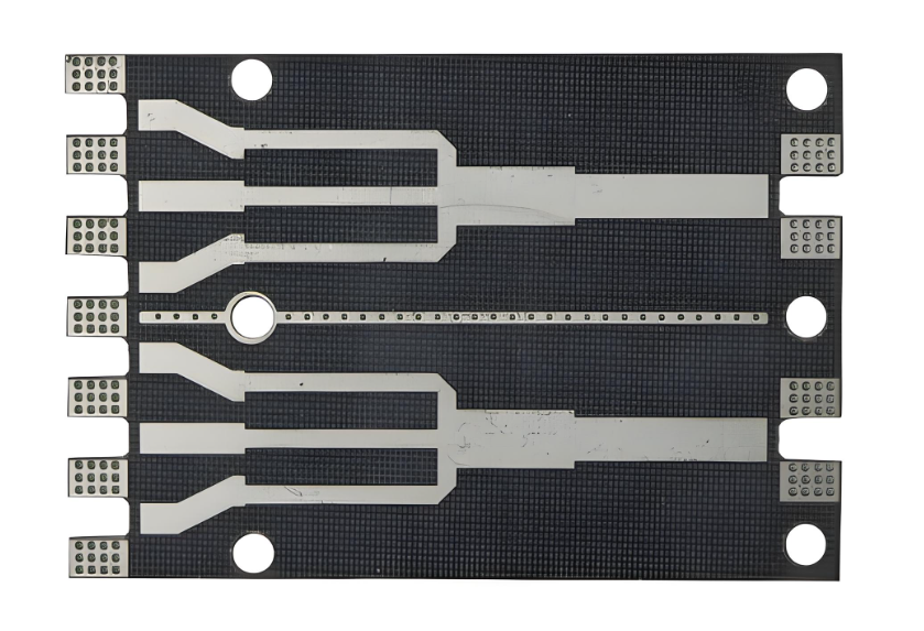
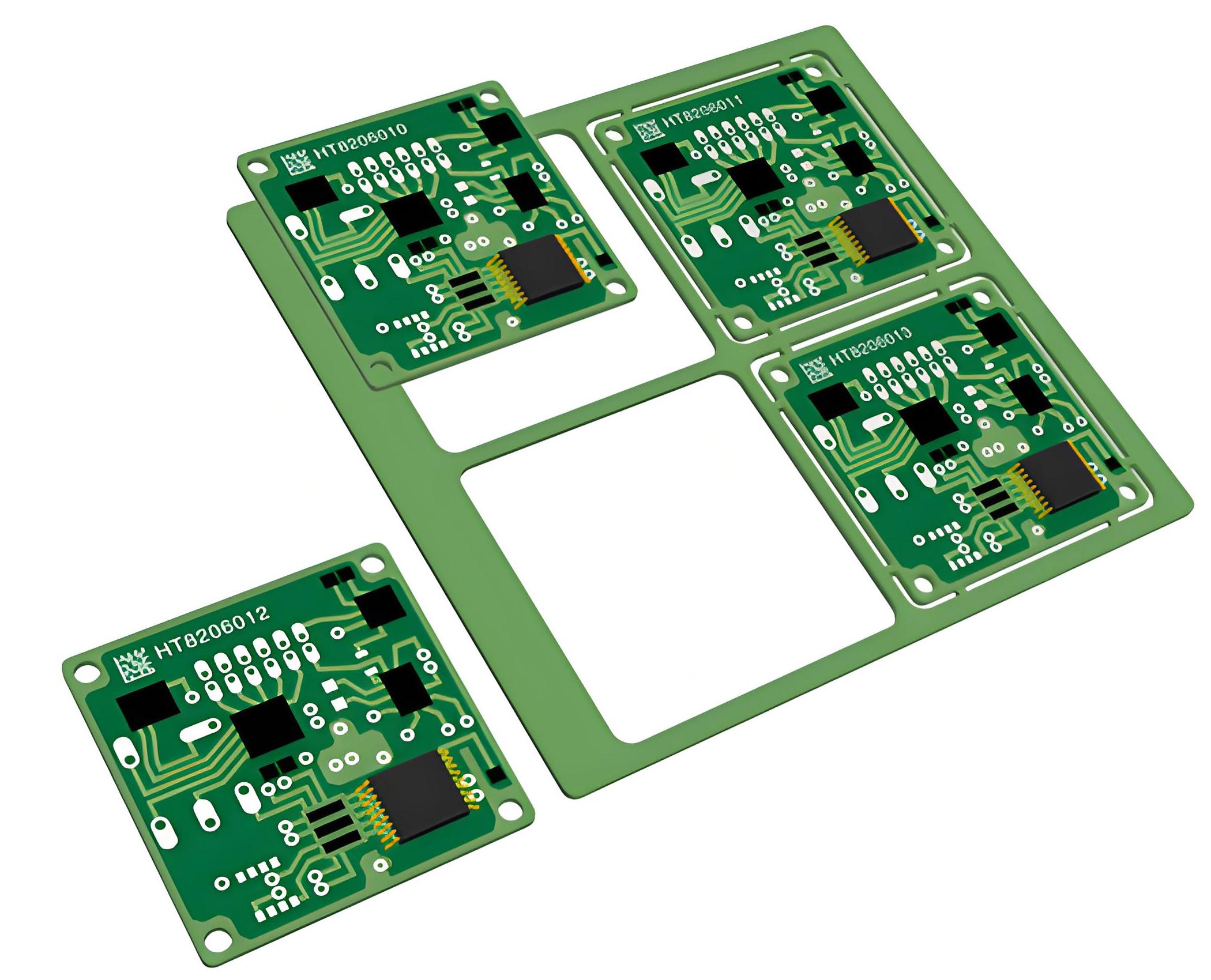
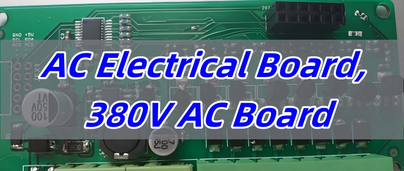
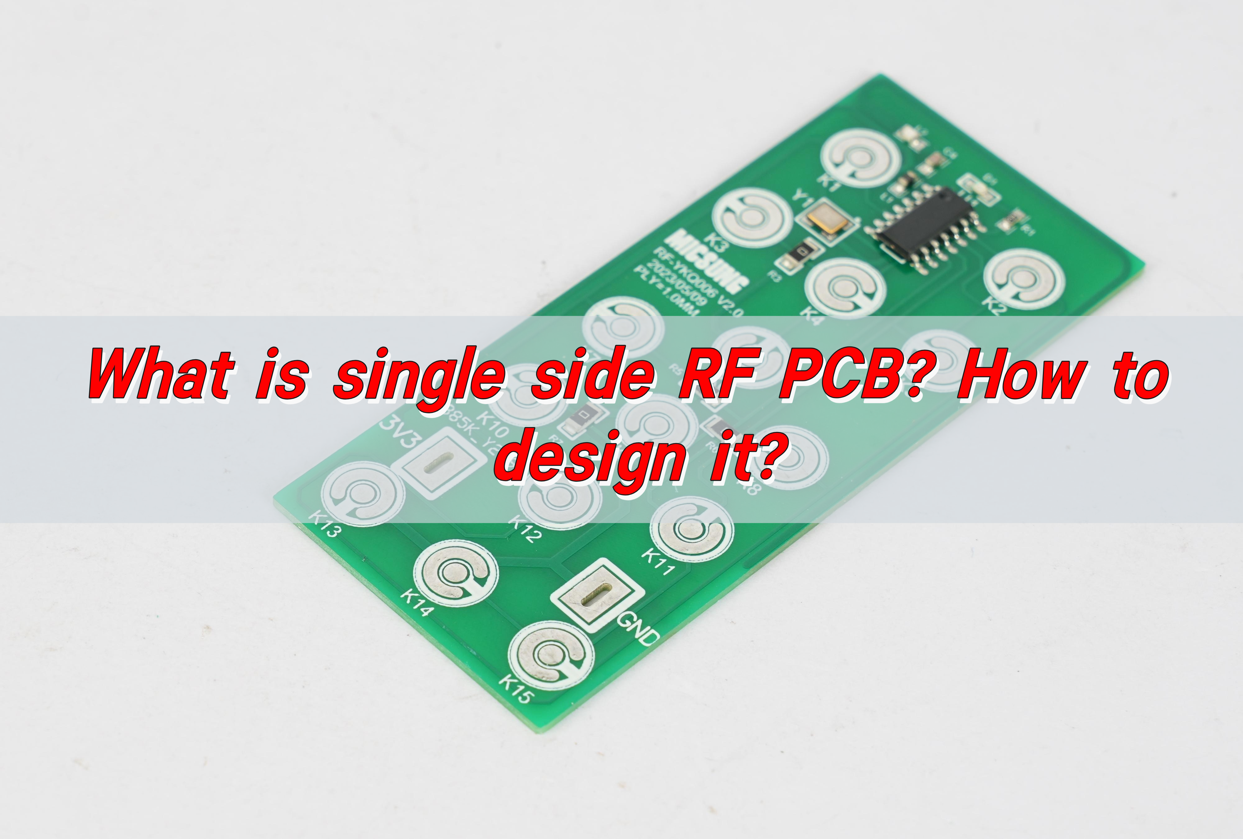
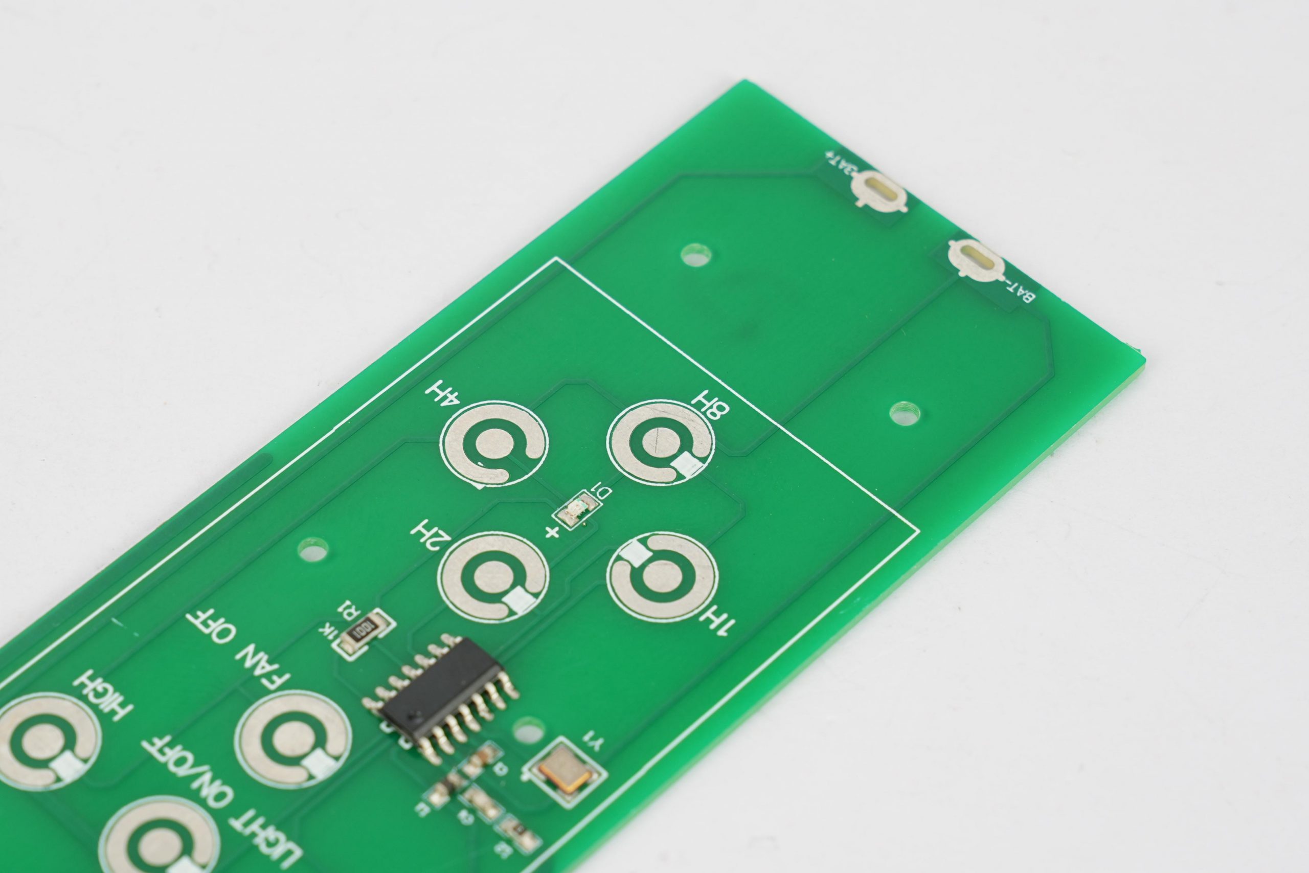
Single Side RF PCB is a radio frequency printed circuit board with all components and traces located on one side of the PCB. This design is usually used for simpler radio frequency applications, such as wireless communication devices, IoT devices, etc. The main features of single-sided RF PCB are low cost, easy installation, and high signal transmission quality.
What is Single Side RF PCB?
A single-side RF PCB is a type of PCB with conductive traces on only one side. The other side is typically non-conductive. These boards are widely used in RF circuits where simple layouts and minimal layers are sufficient for signal transmission.
Unlike double-sided or multi-layer RF PCBs, a single-side RF PCB has a straightforward structure. It consists of a dielectric substrate with a layer of conductive material, usually copper, on one side. Components are mounted on this conductive side, and signal paths are carefully designed to minimize losses.
What are the Types of RF PCBs?
RF PCBs come in various configurations based on material, layer structure, and frequency handling capabilities. The most common types include:
- Single-Sided RF PCB – A basic design with a conductive layer on one side, used in simple RF applications.
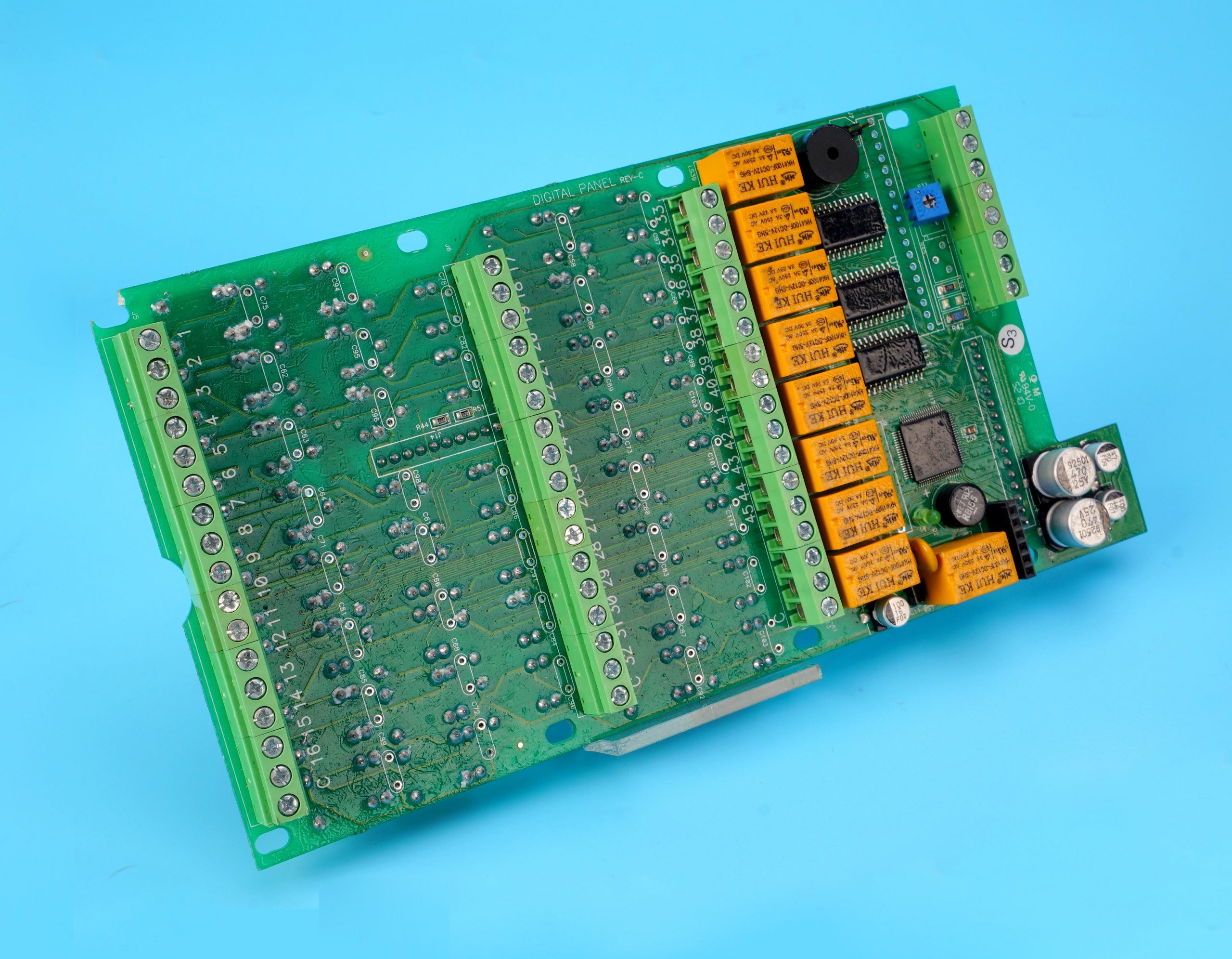
- Double-Sided RF PCB – Features conductive layers on both sides, allowing for more complex circuit designs.
- Multi-Layer RF PCB – Contains multiple layers of conductive material and dielectric, providing enhanced signal performance.
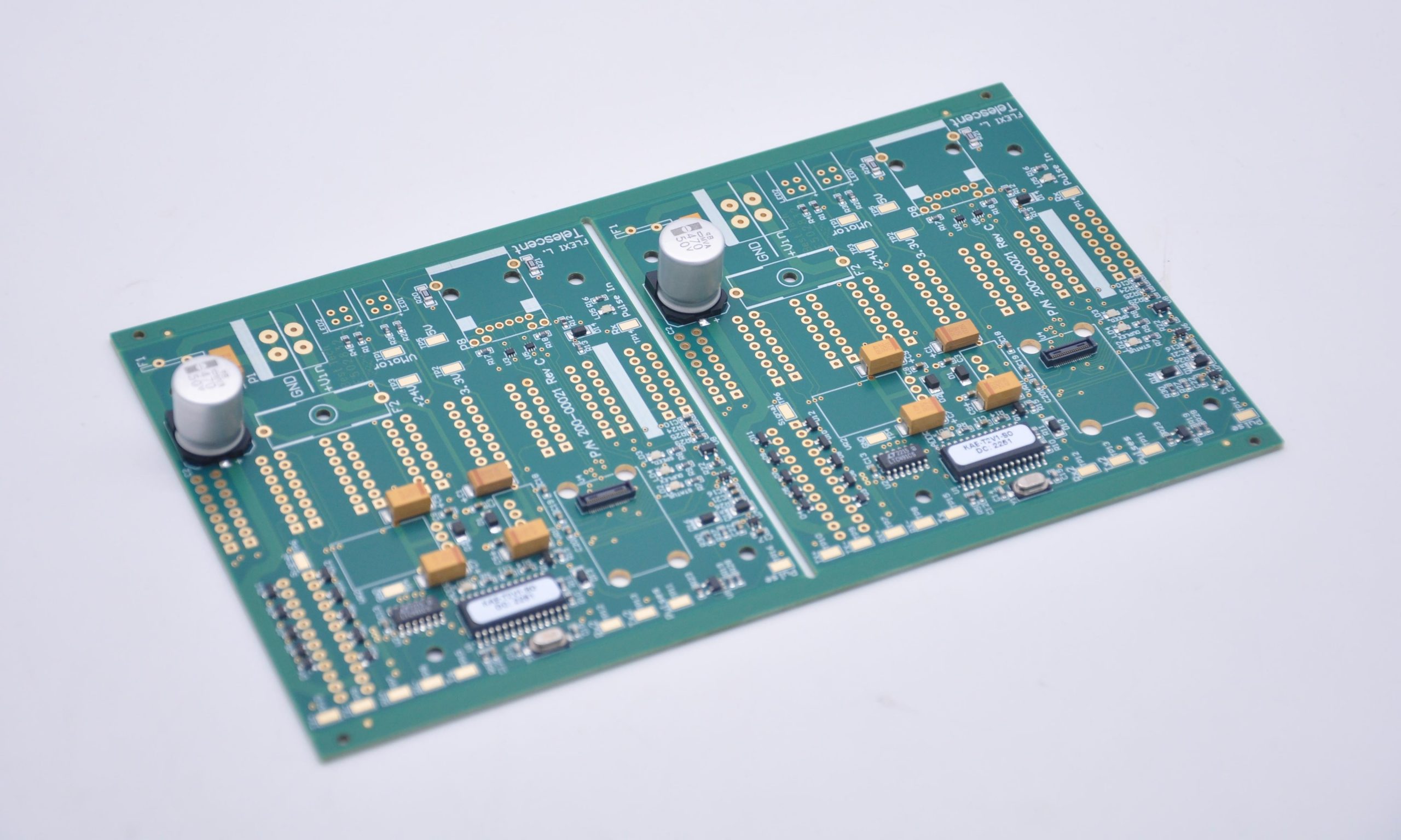
- Rigid RF PCB – Made from solid, inflexible materials, ensuring durability in high-frequency applications.
- Flexible RF PCB – Designed with bendable materials, ideal for compact or dynamic applications.
Each type serves different needs based on frequency range, power levels, and circuit complexity.
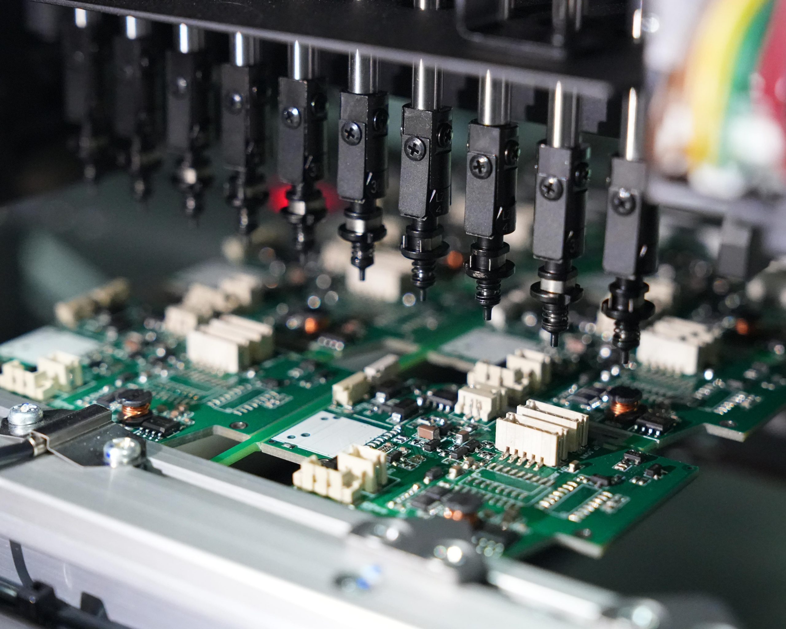
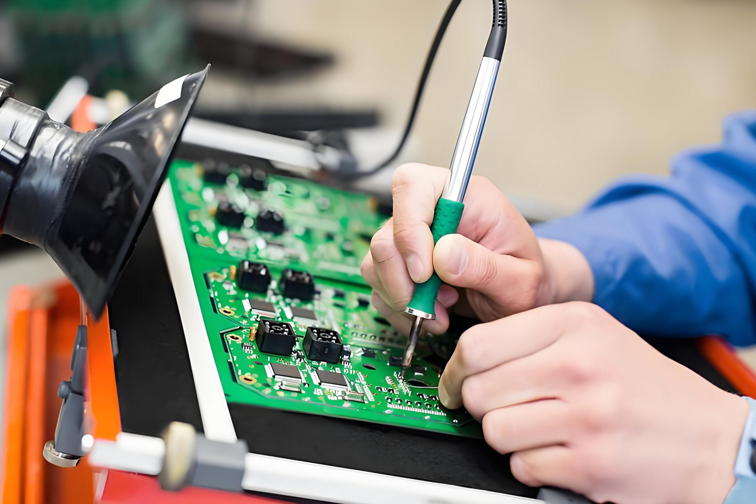
How to Manufacture Single Side RF PCB?
The manufacturing of a single-side RF PCB follows a well-defined process:
- Material Selection – A suitable dielectric material such as FR-4, PTFE, or ceramic is chosen based on frequency requirements.
- Copper Cladding – A thin layer of copper is laminated onto one side of the substrate.
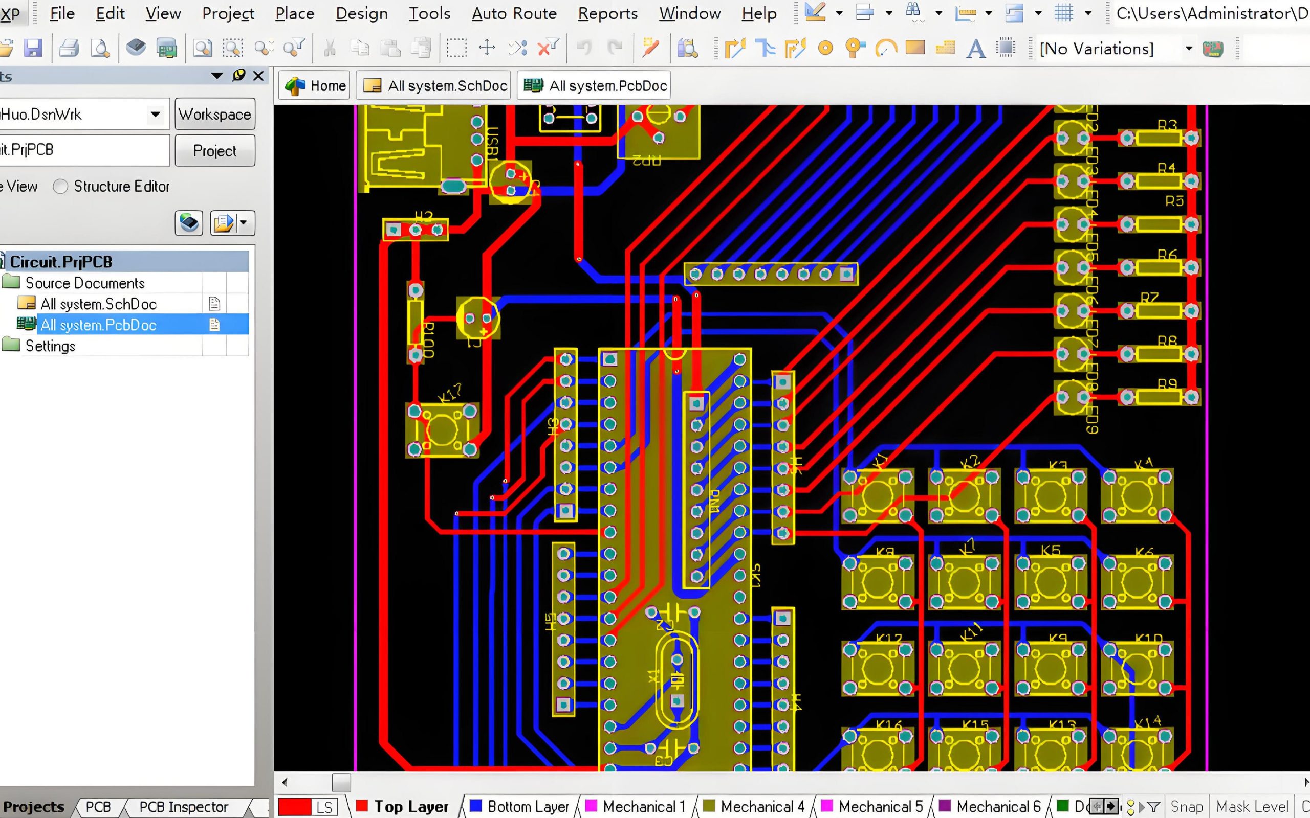
- Circuit Patterning – The required circuit layout is printed onto the copper surface using photolithography or screen printing.
- Etching – Unwanted copper is removed using chemical etching, leaving behind the designed circuit traces.
- Drilling – Holes are drilled for mounting components.
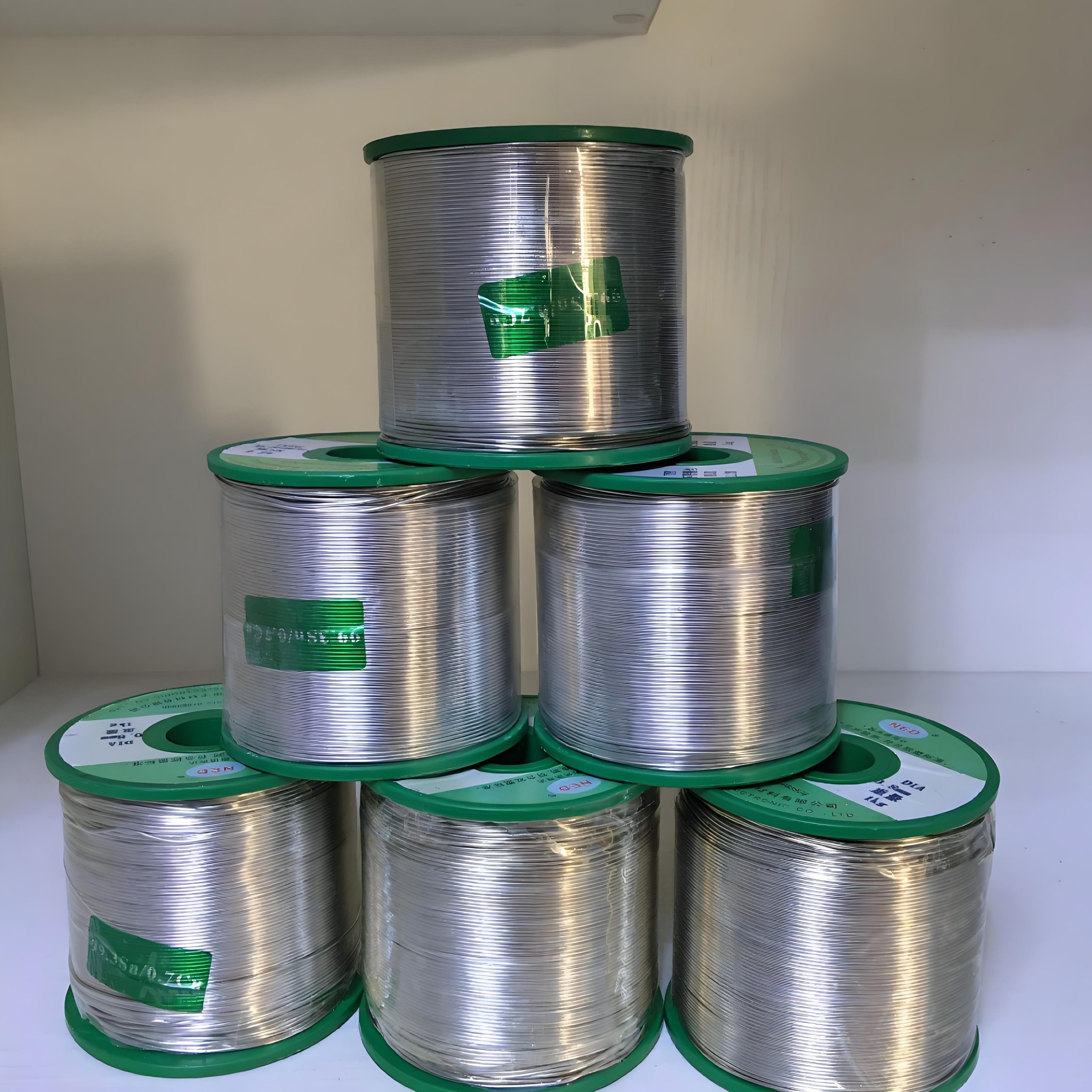
- Surface Finish Application – Protective coatings like ENIG (Electroless Nickel Immersion Gold) or HASL (Hot Air Solder Leveling) are applied to improve durability and solderability.
- Quality Inspection – The finished PCB undergoes electrical and visual testing to ensure performance.
The process ensures that single-side RF PCBs maintain signal integrity and minimize interference.
What to Pay Attention to When Designing Single Side RF PCB?
Designing a single-side RF PCB requires precision to avoid signal loss and interference. Here are key considerations:
- Substrate Material – The dielectric constant (Dk) should be low and stable to reduce signal attenuation. PTFE and Rogers materials are popular choices.
- Trace Width & Spacing – Proper trace dimensions help maintain impedance control and reduce signal distortion.
- Component Placement – High-frequency components should be positioned to minimize signal path length and interference.
- Impedance Matching – Transmission lines should be designed to match impedance, preventing signal reflections.
- Shielding & Isolation – Sensitive signals should be shielded to avoid external interference.
Careful design ensures the PCB delivers reliable RF performance without excessive signal losses.
What are the Advantages of RF PCB?
RF PCBs offer several benefits, making them ideal for wireless and high-frequency applications:
- High-Frequency Performance – Designed for stability in GHz-range signals.
- Low Signal Loss – Special materials reduce power loss during transmission.
- Lightweight & Compact – Suitable for space-constrained applications like IoT devices.
- High Thermal Stability – Can withstand temperature fluctuations without affecting signal integrity.
- Reliable Signal Transmission – Minimizes interference, ensuring clean RF communication.
These advantages make RF PCBs essential for applications like telecommunications, aerospace, and automotive radar systems.
What are the Disadvantages of Single-Sided RF PCB?
While single-side RF PCBs have many benefits, they come with certain limitations:
- Limited Circuit Complexity – Not suitable for highly complex RF systems requiring multiple layers.
- No Ground Plane – Can lead to increased interference and signal integrity challenges.
- Higher Losses Compared to Multi-Layer PCBs – Single-layer designs may have more power dissipation.
- Lower Component Density – Space constraints limit the number of components that can be placed on the board.
Despite these drawbacks, they remain a cost-effective choice for simple RF designs.
What are the Applications of RF PCB?
RF PCBs play a critical role in various high-frequency applications. Some common uses include:
- Wireless Communication – Used in antennas, Wi-Fi modules, and cellular base stations.
- Radar Systems – Essential in automotive radar, military radar, and weather monitoring.
- Medical Devices – Found in MRI machines, wireless patient monitoring, and diagnostic equipment.
- Aerospace & Defense – Utilized in satellite communication and military-grade RF applications.
Their ability to maintain signal integrity in high-frequency environments makes them indispensable in modern electronics.
Conclusion:
Single-side RF PCBs are a crucial component in radio frequency applications. They provide cost-effective and efficient signal transmission for various industries. While they have some design limitations, their advantages in simplicity and performance make them a reliable choice for many RF systems.
For high-quality RF PCB solutions, contact sales@bestpcbs.com. Whether you need single-side, double-sided, or multi-layer RF PCBs, expert support is available to meet your requirements.