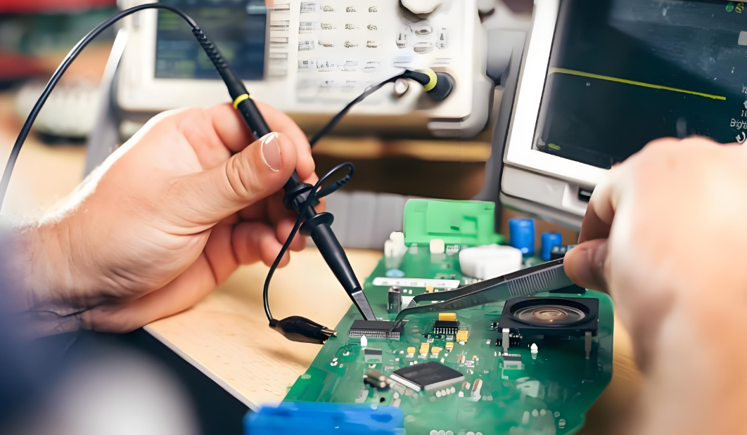
High speed PCB routing plays a critical role in signal integrity, system performance, and EMI control. When designing boards that operate at higher frequencies or faster edge rates, simple routing mistakes can lead to severe issues—such as signal reflections, timing delays, and crosstalk.
To help engineers and designers avoid these common pitfalls, we’ve outlined the 11 most effective high-speed PCB routing practices to keep your circuits stable and reliable.
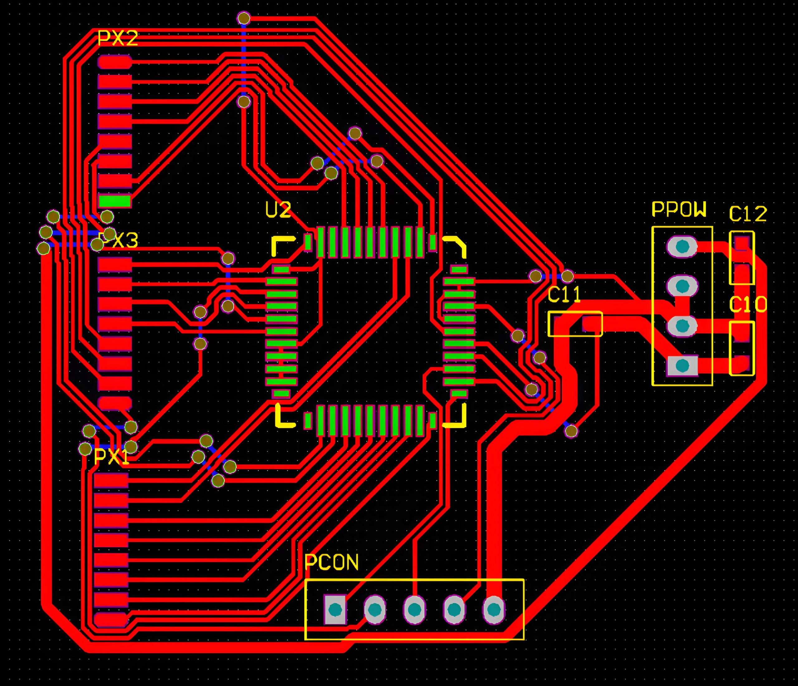
1. Use Short and Direct Signal Paths
In high-speed designs, longer traces become transmission lines. This causes delays and possible signal degradation. The longer the path, the more distortion your signal might encounter. That’s why you should keep all critical nets—like clocks, differential pairs, and high-speed data lines—as short and direct as possible.
For example, a 2-inch trace might seem negligible, but at 5Gbps speeds, even a small delay could impact timing budgets. The best routing practice is to go from point A to point B without meandering.
2. Maintain Controlled Impedance
High-speed signals don’t just travel—they reflect if the impedance isn’t consistent. This is where controlled impedance routing comes in. You need to maintain a specific impedance value (typically 50Ω for single-ended or 100Ω for differential signals).
To achieve this:
- Choose the correct trace width based on the PCB stackup.
- Keep dielectric thickness uniform.
- Avoid inconsistent copper weights.
EBest Circuit (Best Technology) helps you calculate and verify impedance before production using simulation tools and TDR measurements.
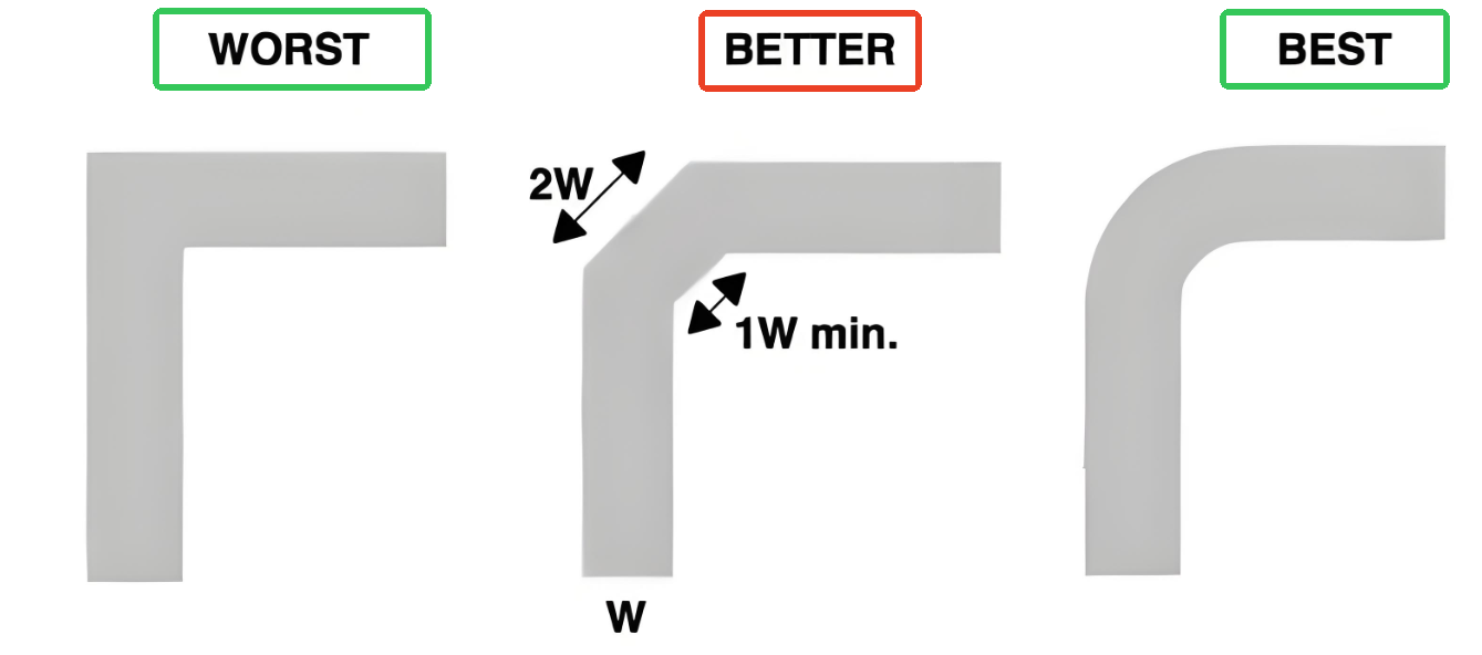
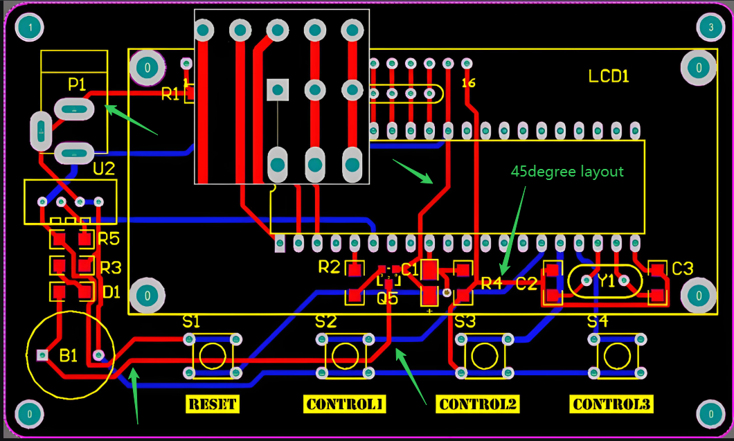
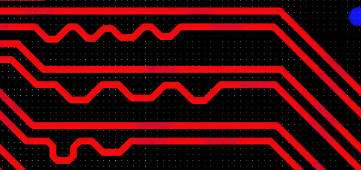
3. Avoid 90-Degree Trace Bends
Sharp bends look neat, but at high frequencies, they act like mini antennas. A 90-degree corner changes the trace width at the bend, creating impedance discontinuity and increasing EMI.
Instead of sharp corners, route traces using:
- Two 45-degree angles
- Or a smooth arc
This method maintains uniform impedance, reduces reflections, and looks cleaner from a manufacturing standpoint.
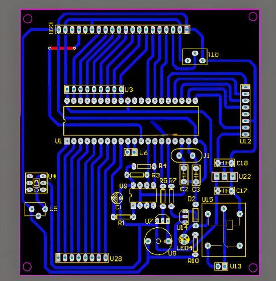
4. Implement Solid and Continuous Ground Planes
Every signal needs a return path, and that path usually travels directly under the trace on the ground plane. If that plane is broken or has cutouts, the return path becomes longer and induces unwanted noise.
To fix this:
- Place a solid, unbroken ground plane beneath high-speed layers.
- Avoid crossing plane splits with high-speed signals.
- Minimize layer transitions that force return paths to detour.
EBest Circuit (Best Technology) uses dedicated ground planes and simulation validation to ensure return paths are uninterrupted.
5. Match Lengths of Differential Pairs
Differential pairs, such as USB, HDMI, or LVDS lines, must be length-matched to prevent signal skew. If one trace is longer than the other, the timing mismatch can cause errors.
Some tips:
- Match lengths to within a few mils.
- Maintain consistent spacing (edge-to-edge).
- Route them together, avoiding different layers unless absolutely needed.
At EBest Circuit (Best Technology), we support tight differential pair matching down to ±5 mil during production.
6. Minimize the Use of Vias
Every via adds capacitance and inductance, which degrades signal quality. High-speed signals don’t like jumping between layers unless absolutely necessary.
If you must use vias:
- Keep them short and consistent.
- Avoid unnecessary layer transitions.
- Use via stitching to maintain continuous return paths.
Our engineering team optimizes via placement and offers blind and buried vias for complex HDI boards to reduce signal loss.
7. Use Proper Termination Techniques
Termination prevents reflections and stabilizes high-speed signals. Whether it’s series, parallel, or AC termination, it depends on your driver and load setup.
For instance:
- Series termination works well for point-to-point connections.
- Parallel termination helps in multi-drop setups.
Improper termination can cause overshoot, ringing, or logic errors. We assist customers in selecting proper termination resistors during DFM review.
8. Isolate Analog and Digital Grounds
Mixing analog and digital signals is risky. Digital circuits generate switching noise that can interfere with sensitive analog components.
Good layout practices include:
- Keeping analog and digital circuits physically separated.
- Avoiding crossover between analog and digital return paths.
- Using ground islands connected at a single point if necessary.
Our layout reviews always evaluate signal isolation to avoid interference in mixed-signal boards.
9. Route Differential Pairs Together
Differential pairs must be routed together, in parallel, and on the same layer. If one signal strays away or loops, it creates an imbalance, which defeats the benefit of differential signaling.
Also:
- Avoid routing them across split planes.
- Keep them tightly coupled (consistent spacing).
- Avoid fan-out unless necessary at termination points.
Our advanced PCB manufacturing equipment keeps tight trace spacing and alignment even on high-density interconnects (HDI).
10. Observe Return Current Paths
High-speed return currents don’t follow the shortest path—they follow the path of least inductance, usually right beneath the trace.
Interrupting that path causes:
- Ground loops
- Crosstalk
- Increased EMI
To prevent this:
- Avoid crossing plane splits with signal traces.
- Use stitching vias to keep the return path near.
- Place decoupling capacitors close to where the signal changes layer.
We validate return paths during layout verification using signal integrity tools.
11. Use Stitching Capacitors and Ground Vias
To suppress high-frequency noise and EMI:
- Use stitching capacitors between power and ground.
- Place ground vias near signal transitions and connectors.
- These components act like firewalls, keeping noise from traveling across the board.
We help customers determine the best placement for decoupling caps and ground stitching to maintain signal purity.
Why Trust EBest Circuit (Best Technology) for Your High-Speed PCB Projects?
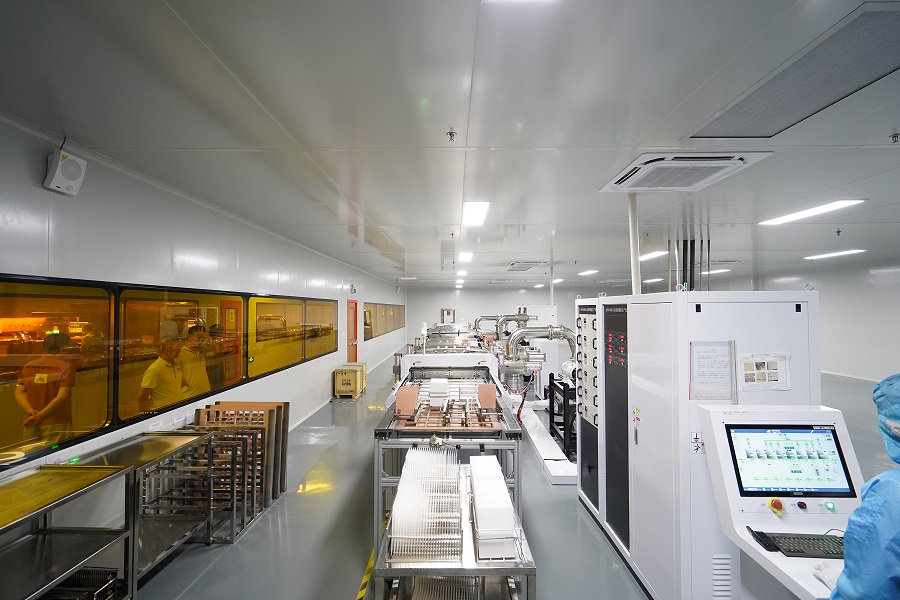
At EBest Circuit (Best Technology), we specialize in advanced PCB manufacturing and assembly solutions, supporting industries like automotive, aerospace, medical, and telecom. With ISO-certifications, we bring rigorous quality control to every project.
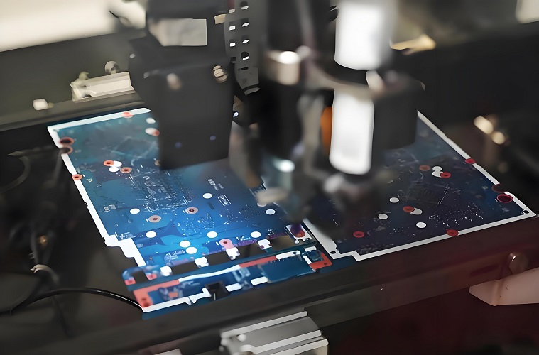
Since its establishment in 2006 as a printed circuit board manufacturer, EBest Circuit (Best Technology) has focused on high-quality, low to medium-volume PCB fabrication, PCB assembly and electronics manufacturing. Our products and services include 1-40 layers printed circuit boards, thru-hole assembly, SMT assembly including BGA assembly, components sourcing, turnkey box build and electronic product development. Whether you need quick-turn prototypes or volume production with controlled impedance, we’re your reliable partner in high-speed design.
Want Reliable High-Speed PCBs? Contact EBest Circuit (Best Technology) Today!
High-speed PCB design is more than just routing—it’s about understanding physics, signal behavior, and layout strategy. At EBest Circuit (Best Technology), we not only manufacture your boards, but also optimize them for real-world performance.
Whether you need HDI PCBs, controlled impedance, differential pair routing, or quick prototypes, our team is ready to help.
👉 Let’s turn your next design into a high-speed success. Contact us now to get a quote or design consultation!
Frequently Asked Questions (FAQs)
1. What is considered a high-speed signal in PCB design?
Any signal with a rise/fall time below 1ns or operating above 100MHz is considered high-speed, as it starts behaving like a transmission line.
2. Can I use auto-routing for high-speed signals?
Auto-routers are not recommended for high-speed nets. Manual routing provides better control over trace length, impedance, and matching.
3. What is skew in differential pairs?
Skew refers to the time delay between the two signals in a differential pair. Skew can cause data errors and must be minimized.
4. How do I calculate trace impedance?
Trace impedance depends on trace width, thickness, dielectric height, and PCB material. Use online calculators or simulation tools like Polar or Altium.
5. Can I run high-speed signals on outer layers?
It’s better to route high-speed signals on internal layers between solid ground planes to reduce EMI and maintain impedance.