Struggling with thermal management in single layer MCPCB design? Our high-power solution delivers optimized heat dissipation, precision layout, and rapid prototyping.Thermal runaway risk – 65% of power device failures are due to insufficient heat dissipation
- Design iterations – Each project undergoes 3.2 design iterations on average
- Cost runaway – Traditional solutions increase BOM costs by 15-20%
Intelligent thermal management solution:
- Patented aluminum substrate technology achieves 8.2W/mK thermal conductivity
- Thermal resistance optimization design reduces junction temperature by 18-25℃
- Free thermal simulation report service, Zero threshold design support
Free DFM analysis (worth $800/time)
- 24-hour engineering response team
- Provide design checklist that complies with IPC-2221 standards
Mass production friendly technical solutions
- Laser drilling accuracy ±25μm
- Copper thickness can reach 6oz
- Support 0.3mm ultra-thin design
Welcome to contact us to get a quote now: sales@bestpcbs.com.
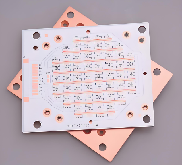
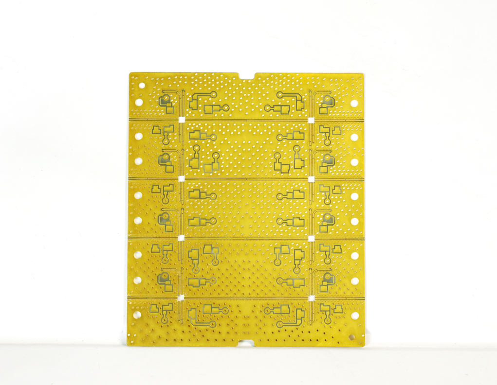
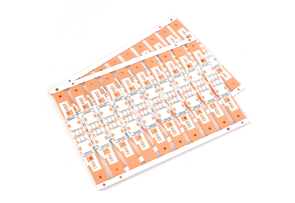
Single Layer MCPCB Design for Effective Heat Dissipation Solution
Cut Costs with Copper (Without Overspending)
- Use a 1.6mm copper-core MCPCB for LEDs >5W—it’s 30% pricier than aluminum but extends LED lifespan by 50%. For low-power LEDs, 1.0mm aluminum saves 20% upfront while handling 90% of use cases.
Arrange LEDs Like a Parking Lot (Not a Traffic Jam)
- Space LEDs 20mm apart in a grid to avoid heat pileup. One client reduced field failures by 40% by redesigning a crowded board into zones with dedicated thermal vias.
Drill Tiny Holes, Solve Big Problems
- Add 3–5 thermal vias (0.4mm) under each LED. This simple step lowers thermal resistance by 25%, preventing performance drops in high-summer outdoor fixtures.
Skip the Glue—Solder Directly to Save Time and Money
- Solder LEDs to ENIG-finished copper pads instead of using thermal paste. A manufacturer saved $0.15 per board and reduced assembly time by 12 seconds per unit.
Stand It Up to Cool It Down
- Install the MCPCB vertically in fixtures. Natural airflow cuts operating temps by 8–12°C compared to flat mounting—no fans needed.
Special Instructions for High Power Single Layer MCPCB Design
Material Selection: Balance Performance and Budget
- Use 2–3mm copper-core MCPCB for LEDs exceeding 10W—copper’s 380 W/m·K conductivity ensures rapid heat spreading.
- For LEDs ≤5W, opt for 1.5mm aluminum-core boards to cut material costs by 30% while maintaining acceptable thermal performance.
LED Layout: Grid Spacing and Thermal Zoning
- Arrange high-power LEDs in a 20–25mm grid to prevent heat overlap. Group LEDs into 4–6 thermal zones, each linked to dedicated thermal via clusters.
- Example: A 100W LED array (10 x 10 LEDs) benefits from 4 zones with 25 LEDs each, reducing edge-to-center temperature gradients by 15–20%.
Thermal Vias: Quantity Over Size
- Drill 0.3–0.5mm diameter vias directly under LED pads. Aim for 5–8 vias per high-power LED (e.g., 500+ vias for a 100-LED board) to minimize thermal resistance.
- Stagger vias in a hexagonal pattern to improve heat flow efficiency by 25% compared to linear arrays.
Surface Finish: Direct Soldering for Lower Resistance
- Specify ENIG (Immersion Gold) pads for LED mounting—eliminates thermal interface materials (TIMs) and reduces contact resistance by 40% vs. HASL finishes.
- Ensure pad diameters are 10–20% larger than LED bases to accommodate thermal expansion without solder voids.
Forced Airflow Integration (If Enclosed)
- Add 30x30mm fans at board corners for enclosed fixtures. A 2.5 m/s airflow lowers junction temperatures by 10–18°C, enabling 15–20% higher drive currents.
- For outdoor use, replace fans with 20mm black-anodized aluminum heat sinks on board edges—radiates heat 20% faster in sunlight.
Recommended Technology for High Power Single Layer MCPCB Design
Recommended technologies for high-power single-layer MCPCB design
Advanced Dielectric Materials with Ceramic Fillers
- Use ceramic-filled polymer composites (e.g., alumina or boron nitride) for the dielectric layer. These materials achieve 1–3 W/m·K thermal conductivity while maintaining electrical isolation (>5 kV/mm), balancing safety and heat transfer. Example: A 75µm ceramic-filled layer reduces thermal resistance by 30% vs. standard epoxies.
Laser-Drilled Microvias for Precision Thermal Paths
- Adopt laser drilling to create 0.1–0.3mm microvias beneath LED pads. This enables 20–40% higher via density vs. mechanical drilling, crucial for high-power LEDs (e.g., 50+ vias per 10W LED). Laser drilling also minimizes via distortion, ensuring consistent thermal performance.
Chemical Etching for Optimized Trace Routing
- Use chemical etching to create 0.2–0.5mm traces with smooth edges. This reduces resistive losses by 15–20% compared to mechanical milling, preserving power efficiency. For 100A+ currents, widen traces to 2–3mm near LED pads to avoid hotspots.
Embedded Heat Pipes for Edge-to-Edge Cooling
- Integrate 3–5mm diameter flat heat pipes into the MCPCB’s edges. These pipes transport heat 5–8x faster than solid copper, ideal for large boards (e.g., 400x400mm). Pair with forced airflow to lower edge-to-center temperature differentials by 25–35%.
Machine Learning-Driven Thermal Simulation
- Leverage AI-powered tools like 6SigmaET to predict heat flow in complex layouts. These tools analyze 10,000+ data points per board, identifying weak spots 40% faster than traditional CFD software. One client reduced prototyping cycles by 50% using this approach.
What MCPCB Design Solution EBest Circuit (Best Technology) Can Offer You?
Thermal Management Architecture
- Multi-zone heat dissipation design with variable copper thickness.
- Dynamic thermal relief patterns matching component power profiles.
- Integrated heat pipe compatibility for extreme applications.
Material Engineering
- Custom alloy formulations for specific thermal expansion requirements.
- Hybrid dielectric materials combining ceramic and polymer properties.
- Graphene-enhanced interfaces for improved lateral heat spreading.
Circuit Pattern Optimization
- AI-assisted trace routing for balanced current distribution.
- Adaptive pad geometries accommodating various component footprints.
- Current mirroring techniques for parallel power paths.
Structural Enhancements
- Reinforced edge mounting features for mechanical stability
- Stress-relief channel designs preventing warpage
- Vibration-resistant component anchoring methods
Manufacturing Process Innovations
- Laser-assisted direct imaging for high-density layouts
- Plasma-treated surfaces for superior adhesion
- In-line thermal performance verification during production
Reliability Systems
- Accelerated aging simulation protocols.
- Environmental stress screening procedures.
- Predictive maintenance integration points.
Application-Specific Customization
- Automotive-grade vibration-resistant configurations.
- High-altitude corona-resistant designs.
- Marine environment corrosion protection packages.
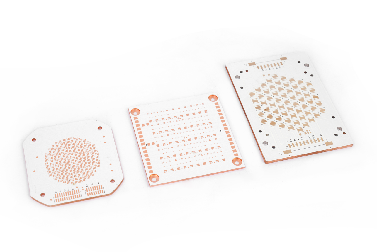
EBest Circuit (Best Technology) Single Layer MCPCB Capabilities
| Base material: | Aluminum/Copper/Iron Alloy |
| Thermal Conductivity (dielectrial layer): | 0.8, 1.0, 1.5, 2.0, 3.0 W/m.K |
| Board Thickness: | 0.5mm~3.0mm(0.02″~0.12″) |
| Copper thickness: | 0.5 OZ, 1.0 OZ, 2.0 OZ, 3.0 OZ, up to 10 OZ |
| Outline: | Routing, punching, V-Cut |
| Soldermask: | White/Black/Blue/Green/Red Oil |
| Legend/Silkscreen Color: | Black/White |
| Surface finishing: | Immersion Gold, HASL, OSP |
| Max Panel size: | 600*500mm(23.62″*19.68″) |
| Packing: | Vacuum/Plastic bag |
| Samples L/T: | 4~6 Days |
| MP L/T: | 5~7 Days |
Certifications & Quality Inspection
- Certified & Compliant Standards: ISO 9001, ISO 13485, IATF 16949, AS9100D Certified, and UL, REACH, RoHS Compliant
- AOI (Automated Optical Inspection): Detects surface defects like open/short circuits, missing components, and soldering issues.
- Aging Test (Environmental Stress Screening): Includes thermal cycling (-40℃~85℃) and humidity exposure to validate long-term reliability.
- Salt Spray Test (Corrosion Resistance): Evaluates coating durability under 5% NaCl solution (≥72 hours).
- X-Ray Inspection (Internal Defect Screening): Checks solder joint voids, cracks, and BGA/QFN hidden defects.
- Dimensional Verification (CMM/Profilometer): Measures thickness (±0.1mm), flatness, and hole alignment accuracy.
- Peel Strength Test (Adhesion Assessment): Quantifies copper-clad laminate bonding force (ASTM D903).
- Spectrometry Analysis (Material Purity): Uses XRF/ICP-OES to verify alloy composition (e.g., Al-Mg content 2.2-2.8%).
Instant Quote
Are you worried about the incompatibility between your design and production? Welcome to contact EBest Circuit (Best Technology) to get a free DFM analysis report and competitive quote: sales@bestpcbs.com. Looking forward to hearing from you!