How to design a metal clad PCB? Let’s discover metal clad PCB’s spec, stackup, material selection and design guidelines, manufacturing process and lead time together.
Are you worried about these problems?
- How to balance thermal efficiency and signal integrity for metal clad PCBs in high-frequency, high-power scenarios?
- How to accelerate reliability validation for complex metal clad PCB structures while reducing prototyping time and cost?
- How to avoid the “trilemma” of performance, cost, and scalability when facing customized metal clad PCB demands?
As a metal clad PCB manufacturer, EBest Circuit (Best Technology) can provide you service and solutions:
- Rapid Prototyping Channel: 72-hour turnaround with integrated simulation tools for zero-delay design verification.
- Thermal Solution Library: Standardized thermal modules + customized thermal management for 30%+ efficiency gain without compromising performance.
- Cost Optimization System: Full-process technical support from material selection to process refinement, achieving 15% cost reduction for customized metal clad PCBs.
Welcome to contact us if you have request for metal clad PCBs: sales@bestpcbs.com.
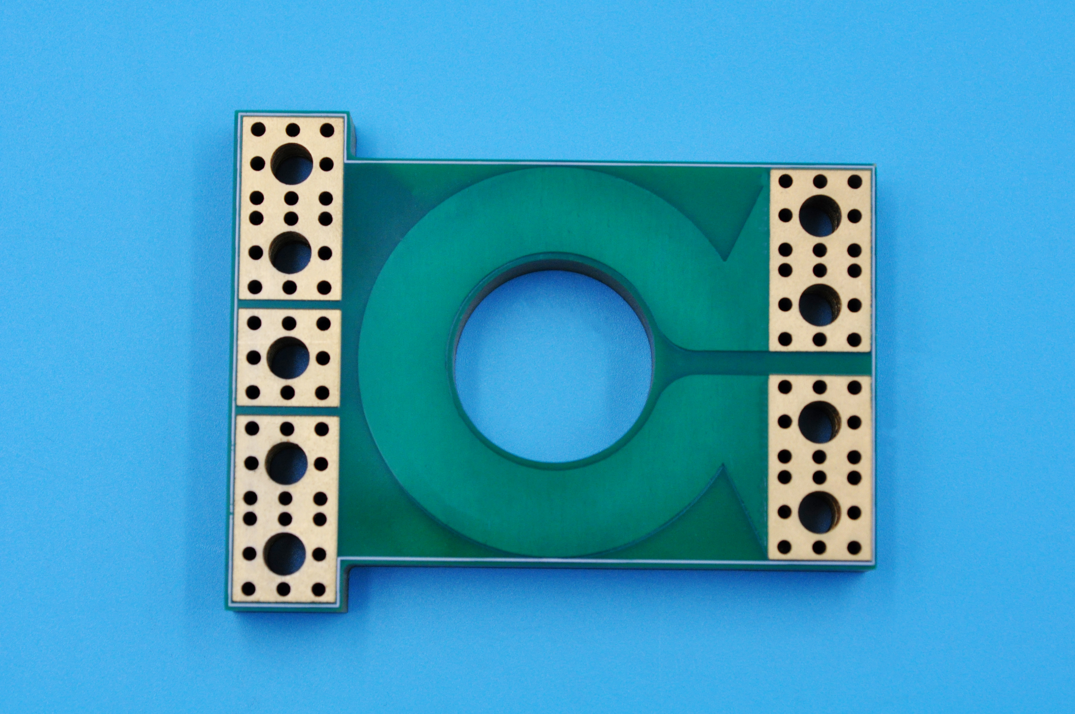
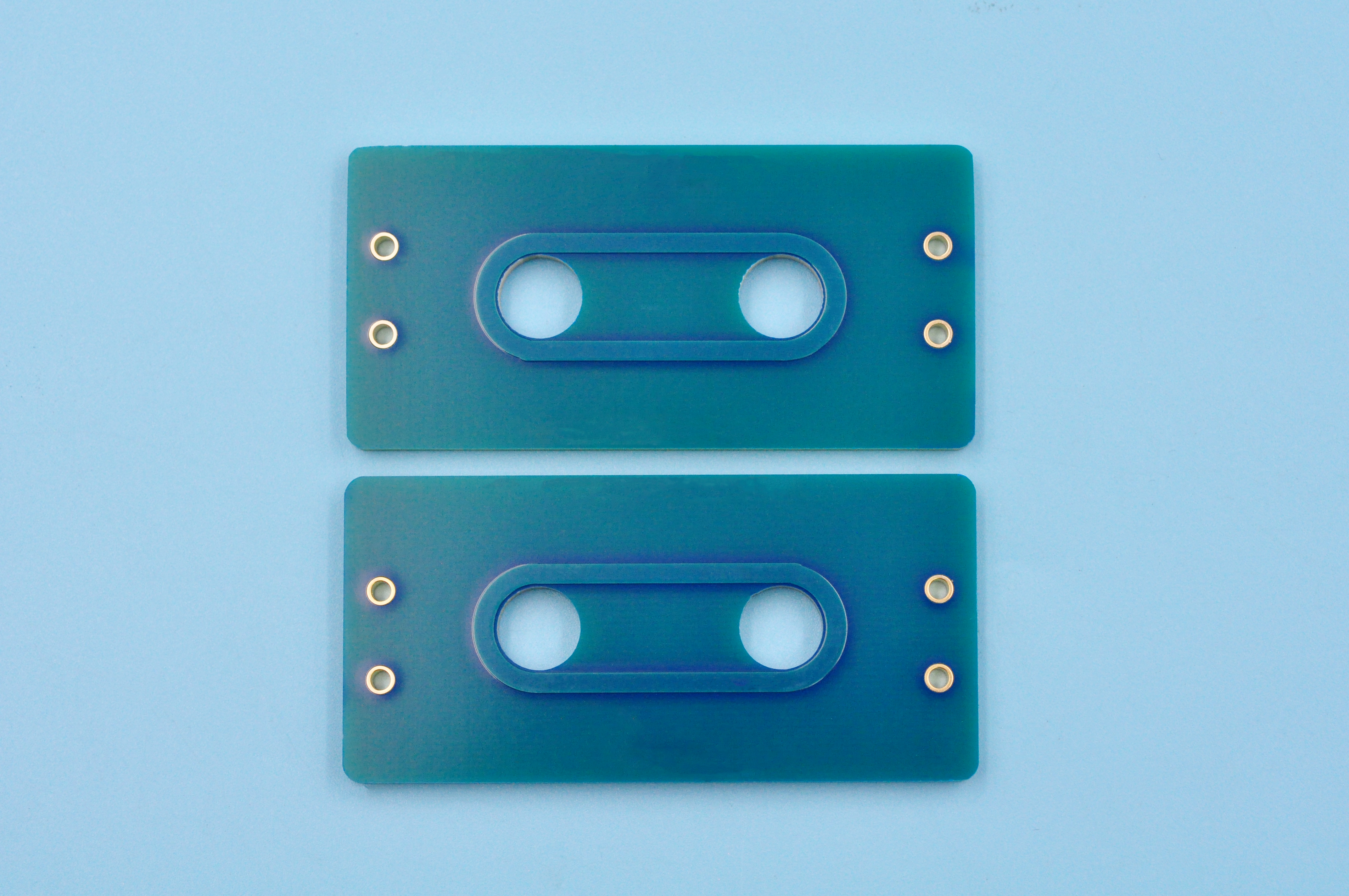
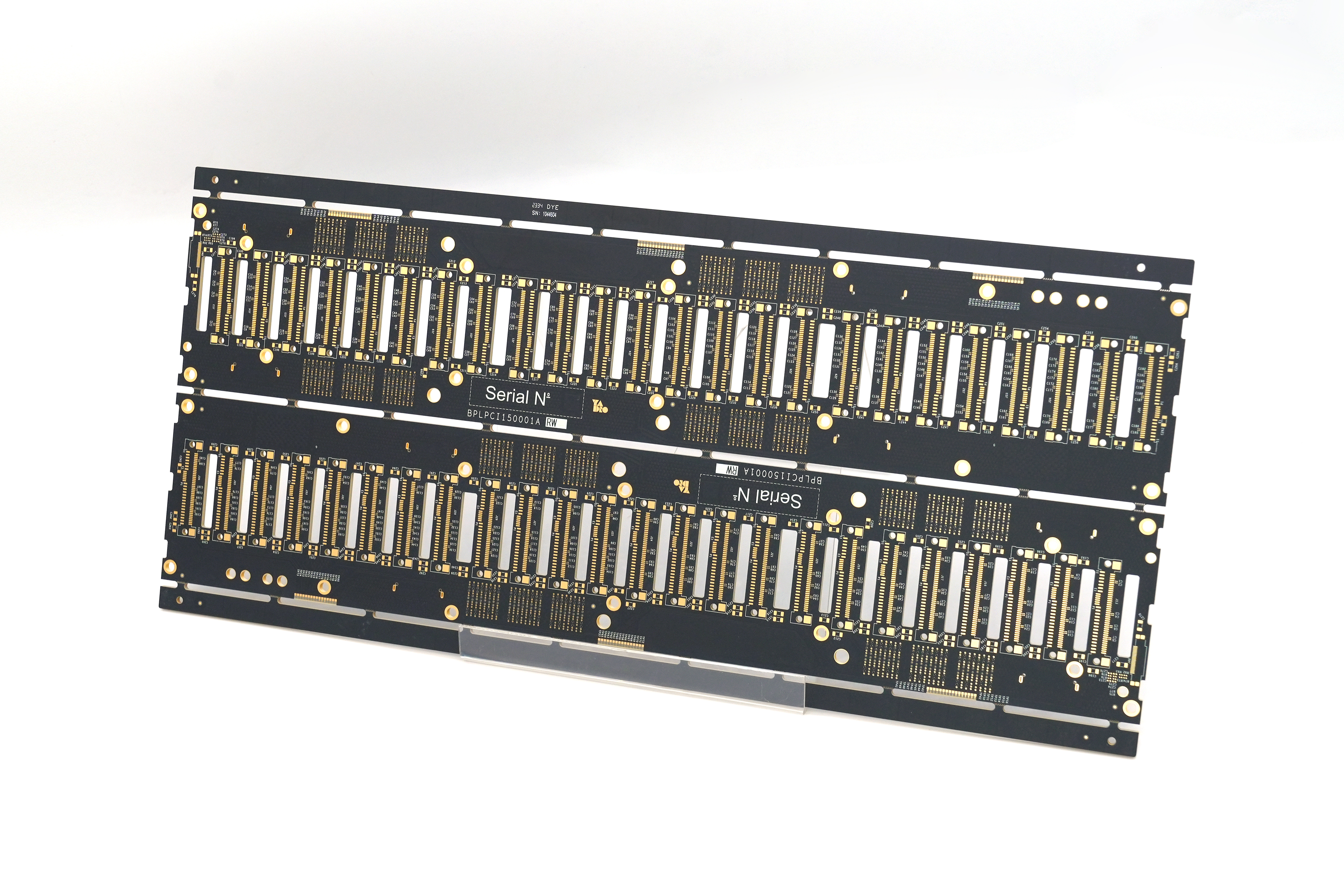
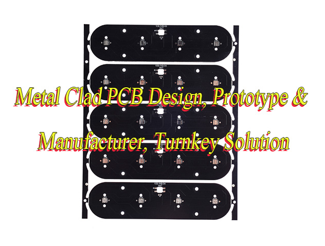
What is Metal Clad PCB?
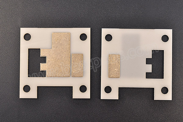
Metal Clad PCB (MCPCB), also known as metal-based copper-clad laminate, is a specialized printed circuit board characterized by replacing traditional FR4 fiberglass substrate with a solid metal plate (typically aluminum or copper). Its structure resembles a three-layer sandwich: the bottom layer is a metal heat-dissipation plate, the middle layer is a thin dielectric and thermal conductive layer, and the top layer is a copper foil layer where circuits are patterned and etched. The primary advantage of this design lies in its exceptional thermal conductivity.
The metal substrate rapidly transfers and dissipates heat generated by high-power components (such as LED chips, power management ICs, and power transistors), effectively preventing thermal-induced component failures. Consequently, MCPCBs are extensively used in high-power, high-heat electronic applications including LED lighting systems, power converters, automotive electronics, and power amplifiers, serving as a critical material for thermal management solutions.
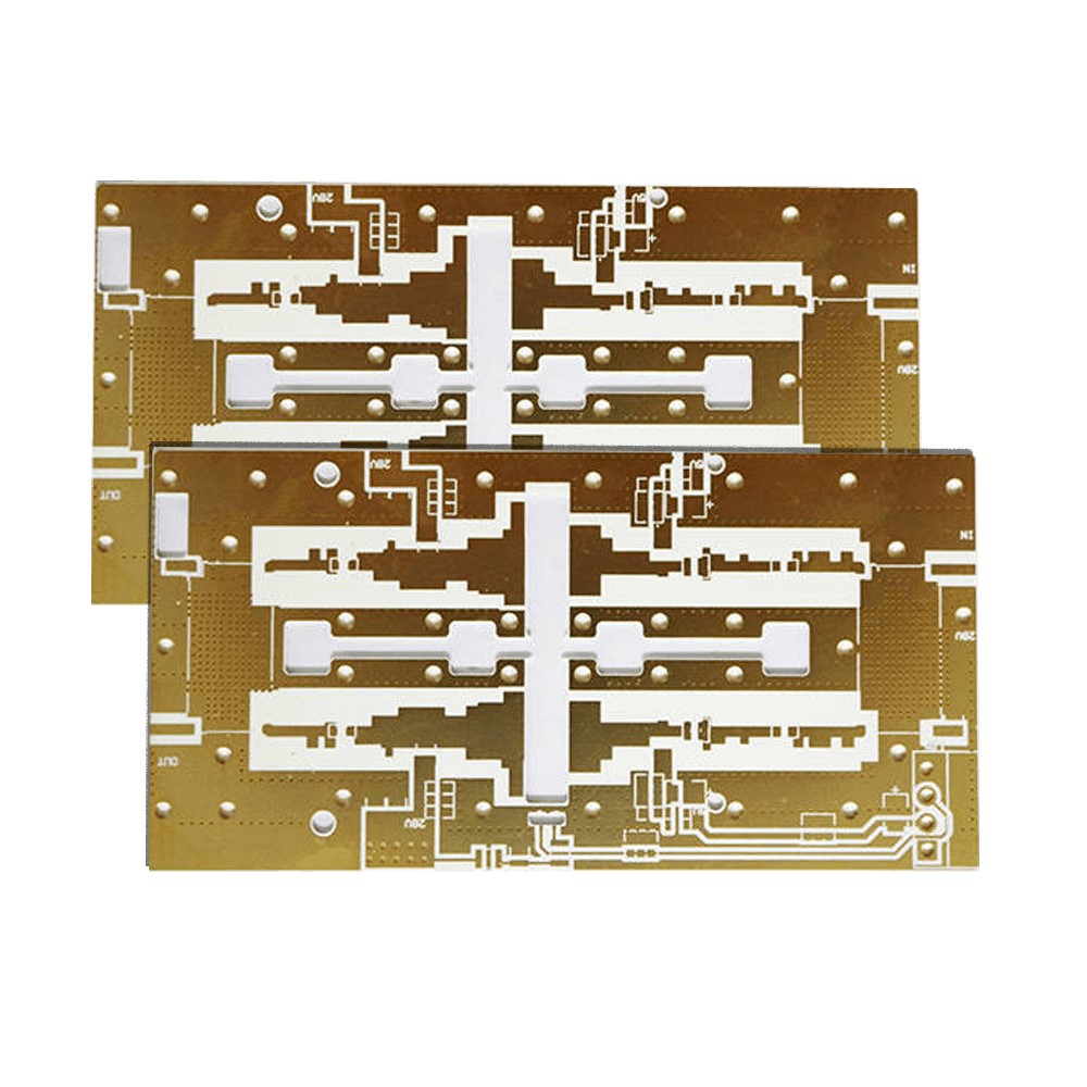
Metal Clad PCB Specifications
| Parameter Category | Aluminum Substrate | Copper Substrate |
| Substrate Material | 6061 Aluminum Alloy | C1100 Pure Copper |
| Thermal Conductivity | 1.0-8.0 W/mK | 2.0-10.0 W/mK |
| Dielectric Strength | 2.5-15 kV | 2.5-15 kV |
| Substrate Thickness | 0.5-5.0 mm | 0.3-3.0 mm |
| Copper Foil Thickness | 1-10 oz (35-350μm) | 1-10 oz (35-350μm) |
| Thermal Resistance (Single Layer) | 0.5-3.0 °C/W | 0.3-2.0 °C/W |
| Maximum Operating Temperature | 130-150°C | 150-200°C |
| Flame Retardant Grade | UL94 V-0 | UL94 V-0 |
| Typical Applications | LED Lighting/Power Modules | High-Frequency Communication/Laser Devices |
Metal Clad PCB Stackup
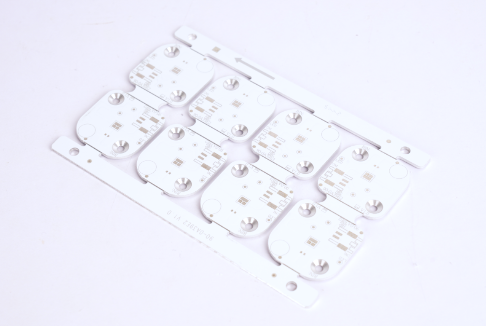
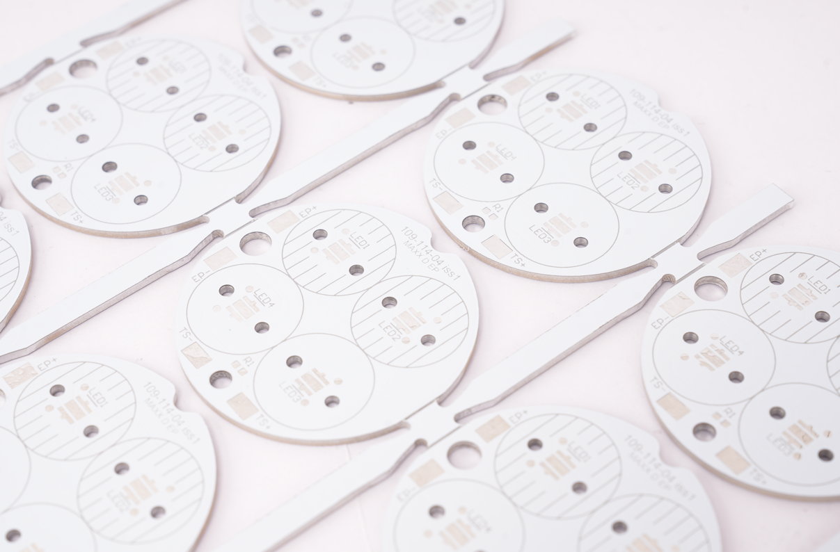
Single-layer MCPCB
- Structure: Copper foil circuit layer → Insulating layer → Metal substrate
- Applications: Widely used in LED lighting modules (e.g., COB substrates), automotive LED DRLs, and compact motor control units for direct heat dissipation in simple circuits.
- Advantages: Low manufacturing cost (30-50% cheaper than multilayer boards); metal substrate acts as direct heat sink with thermal resistance 0.5-1.0°C/W; single-sided routing enables manual/automated assembly for small-batch production.
Double-layer MCPCB
- Structure: Top-layer copper → Insulating layer → Metal substrate → Bottom-layer copper (signal only)
- Applications: Suitable for power conversion modules (e.g., switching power supplies), miniature servo drives, and portable devices requiring dual-layer routing in compact spaces.
- Advantages: Dual-sided routing maximizes space utilization; supports THT/SMT hybrid assembly; shared metal substrate cools both top-layer power devices and bottom-layer components; thermal via design maintains thermal resistance 1.0-2.0°C/W.
Multilayer MCPCB
- Structure: Top-signal layer → Insulating layer → Power/ground layer → Insulating layer → Metal substrate
- Applications: Applied in high-frequency circuits (e.g., 5G filters), medical imaging equipment, and precision instrument control boards needing complex routing and high-performance thermal management.
- Advantages: Layered design integrates power/signal/ground planes; optimized impedance control (±5% tolerance for 50Ω traces); supports high-speed signaling (e.g., PCIe 4.0) with reduced crosstalk; thermal via arrays achieve ≤0.8°C/W thermal resistance; blind/buried vias enhance routing density.
How to Choose Metal Clad PCB Material?
1. Clarify Core Performance Requirements
- Thermal management priority: High-power devices (e.g., LED chips, IGBT modules) require aluminum substrates (150-220W/m·K) or copper substrates (350-400W/m·K) with thermal conductivity ≥2W/m·K. Low-power scenarios (e.g., 1W LED) optimize cost with aluminum.
- Electrical performance matching: Copper substrates (low dielectric loss) for high-frequency circuits (5G filters); copper’s high conductivity (≈58MS/m) for RF applications. Avoid aluminum in high-frequency contexts due to lower conductivity.
- Mechanical strength/weight: Aluminum for lightweight needs (portable devices); copper/stainless steel for high-strength/corrosion-resistant requirements (automotive electronics).
2. Scenario-Based Material Selection Strategies
- LED lighting/power modules: Aluminum dominates for cost efficiency; copper for high-power LEDs (e.g., automotive headlights) with thermal resistance ≤0.8°C/W, extending lifespan by 30%.
- High-frequency/RF circuits: Copper substrates excel in signal integrity with plated-through-hole support; molybdenum (≈138W/m·K) for extreme temperatures (e.g., laser devices).
- Automotive/industrial: Stainless steel for corrosion resistance; copper for vibration resistance (low CTE); thermal-electric separation copper enhances heat dissipation by 40%.
- Medical/precision instruments: Molybdenum/copper for precision routing; halogen-free substrates for biocompatibility.
3. Cost-Process Trade-offs
- Cost-sensitive: Aluminum ($140-420 per square meter) for mass production; copper costs 30-50% more but reduces long-term thermal maintenance.
- Process compatibility: Aluminum requires oxidation coatings; copper supports advanced via technologies; molybdenum needs high-temperature sintering.
- Manufacturing limits: Metal substrates are mostly single-sided; soldering requires preheating to avoid cold joints.
4. Environmental & Reliability Considerations
- Temperature adaptability: Aluminum ≤130°C, copper ≤200°C; molybdenum tolerates >300°C for aerospace/nuclear applications.
- Corrosion resistance: Stainless steel for marine environments; aluminum needs protective coatings.
- Compliance: RoHS-compliant, lead-free solder; medical devices require ISO 10993 biocompatibility.
5. Verification & Optimization Tools
- Thermal simulation: ANSYS Icepak/Flotherm models heat distribution, optimizing paths (via placement, heatsink dimensions).
- Material testing: Labs verify thermal conductivity, CTE, dielectric constant (ASTM D5470 standard).
- Prototyping: Short-lead-time aluminum prototypes (24-hour prototyping services); copper requires thermal conductivity validation.
Metal Clad PCB Design Guidelines
Below is A Detailed Guidelines to Metal Clad PCB Design:
1. Requirement Analysis and Preliminary Planning
- Clarify application scenarios: Confirm with the client the operating environment (temperature range, vibration level, spatial constraints), electrical performance specifications (current capacity, signal frequency, impedance requirements), and reliability targets (lifecycle, acceptable failure rate).
- Define design boundaries: Identify implicit design-impacting factors not explicitly stated by the client (e.g., thermal management priority, cost sensitivity, assembly process compatibility) and document them in a formal design specification.
- Preliminary risk assessment: Based on historical case databases, predict typical failure modes of metal-core PCBs (e.g., thermal stress-induced solder joint cracking, dielectric layer aging) and develop initial mitigation strategies.
2. Layout Planning and Structural Optimization
- Functional zoning principles: Segment regions by signal type (high-speed digital/analog/power) to isolate sensitive circuits from heat sources, ensuring shortest signal paths without cross-interference.
- Heat source placement strategy: Concentrate heat-generating components (e.g., power devices) at the center of the metal-core substrate to leverage its high thermal conductivity for uniform heat dissipation and prevent localized overheating.
- Mechanical structure adaptation: Design positioning holes, mounting slots, and connector locations per client assembly requirements; evaluate thermal expansion coefficient compatibility between the substrate and enclosure materials to avoid assembly stress concentration.
3. Electrical Performance Specialized Design
- Impedance control and signal integrity: For high-speed signal lines, precisely calculate and control characteristic impedance (e.g., 50Ω microstrip), employ differential pair routing, and add ground plane isolation to minimize crosstalk.
- Power integrity management: Design low-impedance power planes, use decoupling capacitor arrays to suppress power noise, and optimize heat dissipation paths for power devices via the metal-core’s thermal conductivity to reduce thermal-electrical coupling effects.
- EMC design: Control electromagnetic radiation and immunity through ground plane segmentation, shielded cavity design, and filter component placement to meet standards (e.g., CISPR, FCC).
4. Thermal Management Design Details
- Thermal simulation and iterative optimization: Utilize thermal simulation tools (e.g., ANSYS Icepak) to build 3D thermal models, predict steady-state/transient temperature distributions, and iterate to optimize heat dissipation paths (e.g., adding thermal vias, adjusting component spacing).
- TIM selection: Choose appropriate thermal interface materials (e.g., pads, grease) based on thermal resistance requirements to ensure good contact and avoid air gaps that increase thermal resistance.
- Forced convection cooling: Where space permits, design heat sinks or fan ducts to combine natural and forced convection for enhanced cooling efficiency in high-power scenarios.
5. Design for Manufacturing/Testing (DFM/DFT)
- Process capability alignment: Confirm metal-core processing capabilities (e.g., minimum hole size, trace/space width, dielectric thickness) with PCB manufacturers to ensure compliance with factory process specifications and avoid manufacturability issues.
- Test point planning: Add test pads or probe access points at critical nodes for in-process electrical testing (e.g., ICT, FCT) and post-repair diagnostics to improve yield and maintainability.
- Documentation and labeling: Clearly mark layer stack-up, solder mask definitions, component polarity, and generate detailed production files (Gerber, pick-and-place) to minimize production errors.
6. Verification & Reliability Testing
- Prototype validation: After engineering sample fabrication, perform electrical testing (impedance, signal integrity), thermal testing (IR thermography, thermal cycling), and mechanical testing (vibration, shock).
- Accelerated reliability testing: Conduct high-temperature/humidity tests, thermal shock tests, and power cycling tests per industry standards (e.g., JEDEC, AEC-Q) to validate long-term reliability and expose design flaws.
7. Design File Export
- File Standardization: Generate industry-standard design packages (Gerber, drill files, BOM, assembly drawings) with clear version control (e.g., RS-274X) for compatibility with manufacturers’ systems. Provide 3D models and footprint libraries to support assembly verification.
- Parameter Annotation: Clearly annotate metal-core substrate layer structure (copper thickness, dielectric parameters), surface finish processes, and special process requirements (e.g., blind/buried via tolerances).
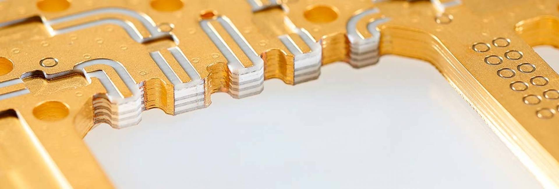
How to Make Metal Clad PCB?
1. Substrate Cutting and Surface Treatment
- Cut the metal-core substrate to design dimensions, perform surface cleaning and roughening treatments (e.g., chemical etching or sandblasting) to enhance adhesion between the metal base and insulating layers. Control surface roughness ≤0.3μm to optimize dry film adhesion.
2. Inner Layer Circuit Fabrication
- Apply dry film → Expose → Develop → Etch (using acidic copper chloride) to form inner layer circuits. Conduct AOI inspection to ensure no breaks/shorts. Perform brown oxidation treatment on copper surfaces to strengthen interlayer bonding.
3. Lamination and Bonding
- Alternately stack inner layer boards with prepreg (PP) sheets, then vacuum-press at 180℃/40kgf/cm² to form a multi-layer structure. Ensure layer symmetry to prevent thermal stress-induced warping. Cure resin in a vacuum environment to eliminate air bubbles, followed by trimming and edge grinding to achieve dimensional accuracy.
4. Drilling and Hole Metallization
- Perform CNC drilling (precision ±0.05mm) or laser micro-drilling (for 0.15mm blind/buried holes). Deburr holes and coat carbon layers as electroplating cathodes. Conduct electroless copper plating (0.3-1μm) → electroplating copper (20-25μm) to achieve conductive holes. Verify coating thickness via X-ray fluorescence.
5. Outer Layer Circuit Fabrication
- Repeat inner layer steps (dry film application, exposure, development, etching) to form outer layer circuits. For metal-core substrates, integrate thermal paths (e.g., thermal vias, heat sinks) leveraging high thermal conductivity.
6. Solder Mask and Surface Treatment
- Apply liquid photosensitive solder mask ink, then UV-expose and develop to create solder mask layers. Perform surface treatments (e.g., ENIG, HASL, OSP) to enhance solderability and corrosion resistance.
7. Thermal Management Design Optimization
- Design thermal paths (e.g., increasing thermal via density, adding heat sinks) based on the metal-core substrate’s high thermal conductivity. Use thermal simulation software to optimize heat dissipation efficiency.
8. Shaping and Cutting
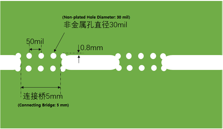
- Use CNC milling or V-Cut to shape the board to design dimensions, ensuring edge smoothness. Clean and dry the boards, with a minimum spacing of 2× board thickness between pieces to prevent adhesion issues.
9. Electrical Testing and Quality Inspection
- Conduct 100% flying probe testing for continuity, AOI/AXI for pad alignment and inner layer defects, and impedance testing (e.g., 90Ω for USB differential pairs) to ensure signal integrity.
10. Packaging and Shipping
- Use vacuum anti-static bubble wrap packaging with desiccant and humidity cards. Secure boards in cartons with thick foam and strapping. Label cartons with part numbers, versions, quantities, and origin. Include quality certificates (solderability reports, test records) and packing lists to ensure dry, shockproof, and ESD-safe transportation.
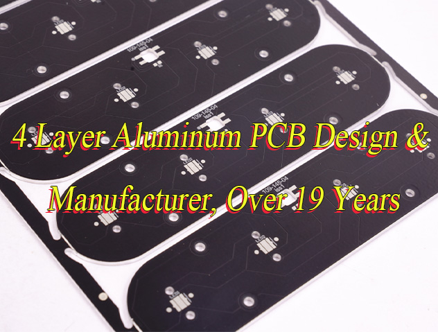
Why Choose EBest Circuit (Best Technology) as Metal Clad PCB Manufacturer?
Reasons why choose us as metal clad PCB manufacturer:
- 19 Years of Expertise: Leverages 19 years of PCB manufacturing experience with a defect database and process knowledge base, reducing client trial-and-error costs by 80% and minimizing production flaws.
- Multi-Industry Certification Backing: Holds medical-grade ISO 13485, RoHS, and IATF automotive certifications, meeting compliance requirements for high-demand sectors like automotive and healthcare.
- Free DFM Design Analysis: Provides complimentary design-for-manufacturing assessments to preempt design risks (e.g., trace/spacing violations), optimize manufacturing efficiency, and reduce post-modification costs—cut client E’s production cycle by 30%.
- Price Competitiveness: Delivers industry-leading cost-effective solutions through supply chain optimization and scaled production, reducing client procurement costs by 15-20% (verified by third-party audit) while enabling precise budget control for projects.
- Cost-Sensitive Design Support: Tailors low-cost design strategies to specific client needs, achieving cost optimization via material substitution (e.g., 30% reduction with aluminum alternatives) and process simplification, thereby enhancing product market competitiveness.
- Rapid Prototyping for Urgent Orders: Offers 24-hour express prototyping services to shorten development cycles, accelerate design validation, and seize market opportunities—successfully advanced client B’s medical device verification by 3 days.
- Efficient Delivery Guarantee: Maintains 99.2% on-time delivery rate (Q3 data) through intelligent production scheduling and logistics collaboration, ensuring end-to-end efficiency from production to delivery.
- Strict Quality Control & Full Inspection: Implements 100% batch inspection paired with ISO 9001/IATF 16949 certifications, achieving defect rates below 0.05% to ensure consistent product quality.
- Rigorous Quality Traceability System: Ensures full process traceability of quality data, complemented by strict quality control procedures, to guarantee batch compliance with international standards like ASTM B25.
- Integrated Turnkey Solutions: Streamlines client supply chain management and boosts project efficiency by 40% through end-to-end solutions spanning design consultation, prototyping, and volume production.
Our Metal Clad Printed Circuit Board Capabilities
| Parameter | Capabilities |
| Base Material | Aluminum/Copper/Iron Alloy |
| Thermal Conductivity (Dielectric Layer) | 0.8 W/(m·K), 1.0 W/(m·K), 1.5 W/(m·K), 2.0 W/(m·K), 3.0 W/(m·K) |
| Board Thickness | 0.5mm~3.0mm (0.02″~0.12″) |
| Copper Thickness | 0.5 OZ, 1.0 OZ, 2.0 OZ, 3.0 OZ, up to 10 OZ |
| Outline Processing | Routing, Punching, V-Cut |
| Soldermask Color | White/Black/Blue/Green/Red Oil |
| Legend/Silkscreen Color | Black/White |
| Surface Finishing | Immersion Gold, HASL (Hot Air Solder Leveling), OSP (Organic Solderability Preservative) |
| Max Panel Size | 600mm × 500mm (23.62″ × 19.68″) |
| Packing Method | Vacuum Packaging/Plastic Bag Sealing |
| Prototype Lead Time (L/T) | 4~6 Days |
| Mass Production Lead Time (MP) | 5~7 Days |
How to Get a Quote for Metal Clad PCBs Project?
Below is a Material List Required for Quotation:
- Design Package: Includes Gerber files, drilling files, BOM list, and process cards to ensure full traceability of manufacturing information and provide precise design basis for quotation.
- Substrate Material Specifications: Specifies metal substrate type (aluminum/copper), thickness, dielectric material, and thermal conductivity requirements (e.g., 150-220W/m·K for aluminum substrates), directly impacting material costs and thermal performance.
- Quantity & Lead Time: Provides order volume, batch delivery schedules, and 99.2% on-time delivery requirements to facilitate production planning and logistics coordination, ensuring efficient delivery.
- Special Process Requirements: Specifies thermal via density (e.g., 15-20 vias/cm²), surface finishes (ENIG/OSP), and high-frequency signal routing rules (e.g., 100±10Ω impedance control), which determine production costs and technical feasibility.
- Quality Certification Requirements: Specifies standards such as ISO 9001, IATF 16949, or medical-grade RoHS-compliant lead-free certification to ensure industry compliance and avoid post-certification risks.
Welcome to contact us if you have any request for metal clad PCBs: sales@bestpcbs.com.