Medical PCB assembly services are the specialized production and system integration of printed circuit boards for life-critical medical equipment. This article explores how partnering with the right provider ensures reliability, compliance, and innovation in healthcare technology.
Developing a new medical device is a high-stakes endeavor. Key Pain Points for Medical Device Developers:
- Regulatory Maze: Navigating FDA, ISO 13485, and IEC 60601 standards without expert guidance is time-consuming and risky.
- Design for Manufacturing (DFM) Gaps: Prototype designs often have hidden flaws that cause failures during volume production.
- Supply Chain Insecurity: Unreliable component sourcing or offshore delays jeopardize project timelines and device availability.
- Inconsistent Quality: Lack of rigorous process controls leads to field failures, recalls, and patient safety risks.
- Prototype Bottlenecks: Slow turnaround times for design iterations critically delay testing, verification, and time-to-market.
These challenges demand a partner with specialized expertise. The following solutions are foundational to a trusted medical electronics manufacturing relationship.
- Proactive Compliance Framework: A partner with ingrained quality systems (ISO 13485 certified) guides you through documentation and validation seamlessly.
- Early DFM/DFA Analysis: Expert engineers review designs pre-production to eliminate errors, enhance reliability, and reduce costs.
- Controlled, Traceable Supply Chain: Using a vetted network of component suppliers and US based PCB assembly capabilities mitigates shortage and geopolitical risks.
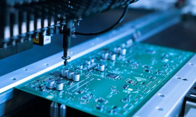
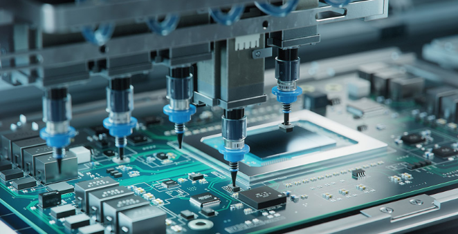
- Robust Quality & Testing Regime: Implementing automated optical inspection (AOI), X-ray, and functional testing ensures every board meets stringent medical-grade specifications.
- Dedicated Rapid Prototyping Lines: Offering quick turn PCB USA services accelerates the design-test-iterate cycle, getting you to clinical trials faster.
EBest Circuit (Best Technology) is a specialized PCB manufacturing and assembly provider focused on the rigorous demands of the medical sector. Our state-of-the-art facility is ISO 13485:2016 certified, and our global production network includes advanced SMT factories in both China and Vietnam. Each site operates under a unified MES-driven manufacturing system, enabling full process traceability, tighter quality control, and consistent performance across all medical projects. Our engineering team is dedicated to merging technical excellence with regulatory mastery, ensuring every medical PCB meets the highest reliability and compliance standards. For a consultation on your next PCBA printed circuit board assembly project, contact us at sales@bestpcbs.com.
How Do Medical PCB Assembly Services Ensure Reliable Performance in Today’s Healthcare Electronics?
Reliable performance in medical electronics is non-negotiable. Medical PCB assembly services achieve this by implementing a multi-layered approach to quality and control that far exceeds commercial standards.
- Medical-Grade Materials & Components: Only using high-Tg laminates, conformal coatings, and components rated for extended life and stable performance in physiological environments.
- Enhanced Process Controls: Strict adherence to controlled procedures for soldering (e.g., lead-free SAC305 profiles), cleanliness (ionic contamination testing), and electrostatic discharge (ESD) protection.
- Comprehensive Testing Protocol: Every board undergoes a battery of tests:
| Test Method | Purpose |
|---|---|
| Automated Optical Inspection (AOI) | Catches soldering defects, missing, or misaligned components. |
| X-Ray Inspection | Verifies integrity of BGAs, internal layers, and via fills. |
| In-Circuit Test (ICT) | Checks electrical performance and component values. |
| Functional Test (FVT) | Simulates the device’s real-world operation. |
- Full Traceability: Lot-by-lot and even board-level tracking of all materials and components is maintained, a critical requirement for FDA audits and potential recall actions.
- Environmental Stress Screening (ESS): Subjecting boards to thermal cycling and burn-in to identify and eliminate early-life failures (infant mortality).
In summary, reliability is engineered through a combination of superior materials, meticulous processes, and exhaustive verification, ensuring devices perform as intended over their entire service life.
What Is the Difference Between PCB Fab and Assembly?
The journey from design to a functional board involves two distinct, sequential phases: fabrication (PCB fab) and assembly (PCB manufacturing and assembly). Confusing them can lead to project missteps.
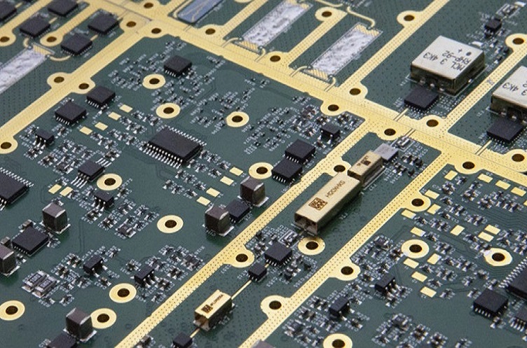
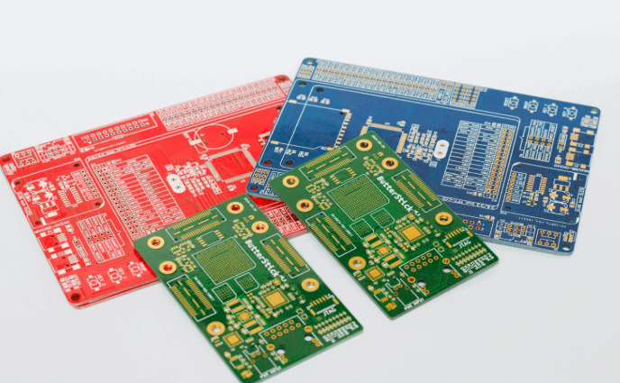
- PCB Fabrication (Fab): This is the process of manufacturing the bare, unpopulated circuit board. It starts with design files (Gerbers) and involves:
- Creating the substrate laminate.
- Imaging and etching the copper layers to form traces.
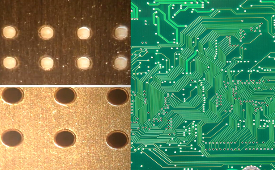
- Drilling holes (vias and through-holes).
- Applying solder mask and silkscreen.
- Performing electrical testing on the bare board.
- Output: A bare PCB with pads and holes, ready for components.
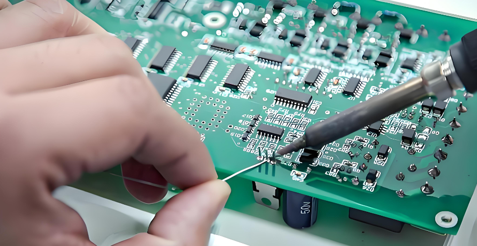
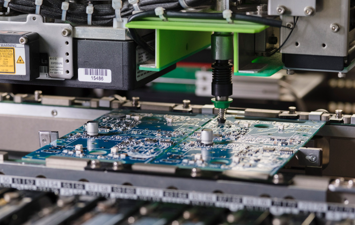
- PCB Assembly (PCBA): This is the process of mounting and soldering electronic components onto the fabricated bare board. It involves:
- Applying solder paste via stencil.
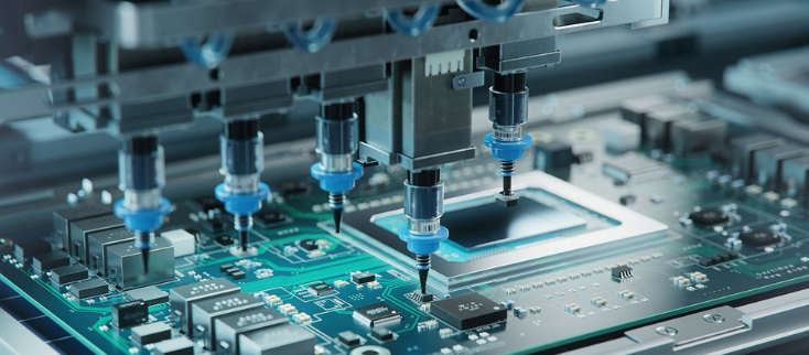
- Placing components (Surface-Mount Technology – SMT) using pick-and-place machines.
- Reflow soldering to create electrical connections.
- Through-hole component insertion and soldering.
- Cleaning, inspection, and functional testing.
- Output: A fully functional, populated printed circuit board assembly.
Think of PCB fab as printing the wiring diagram and PCB assembly as installing all the light switches, outlets, and fixtures. A true turnkey partner, like a professional PCB design company turned manufacturer, expertly manages both phases.
Why Medical PCB Assembly Services Demand Higher Standards Than Conventional PCB Manufacturing and Assembly?
Medical devices directly impact human life, making failure unacceptable. This fundamental truth elevates every requirement from the component level to the final system integration.
- Regulatory Scrutiny: Medical devices require formal approval (FDA, CE). The entire production process must be documented and validated under standards like ISO 13485. A simple process change in conventional manufacturing can become a major, documented change request in medical.
- Extreme Reliability & Longevity: A consumer device may have a 2-3 year life. An implantable or critical care device must function flawlessly for 10-15+ years. This demands higher-grade materials and accelerated life testing.
- Risk Management (ISO 14971): Every potential failure mode must be identified, analyzed, and controlled. The assembly process itself is a critical control point to mitigate risks like short circuits or cold solder joints.
- Biocompatibility & Cleanliness: Devices contacting patients must not leach harmful substances. Assembly processes must ensure extreme cleanliness to avoid ionic contamination that could cause corrosion or failure.
- Traceability: While batch traceability might suffice for consumer goods, medical devices often require component-level traceability to facilitate targeted recalls if a supplier’s component batch is found faulty.
Therefore, medical PCB assembly services are not just about soldering components; they are about executing a rigorously controlled, documented, and validated protocol where quality is measured in patient safety outcomes.
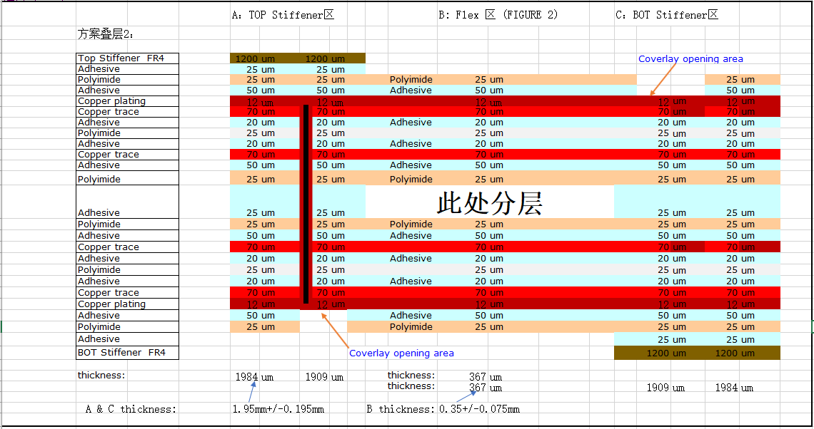
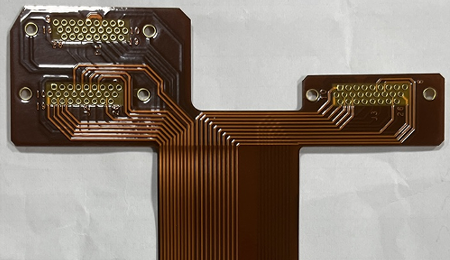
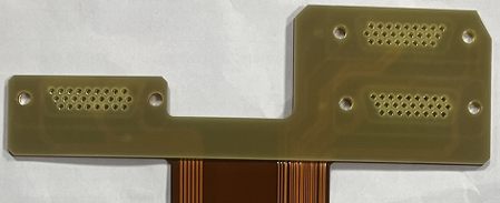
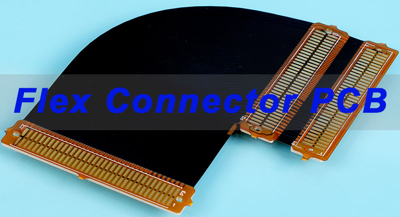
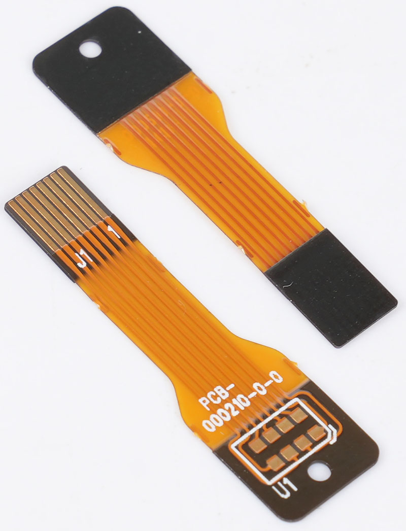
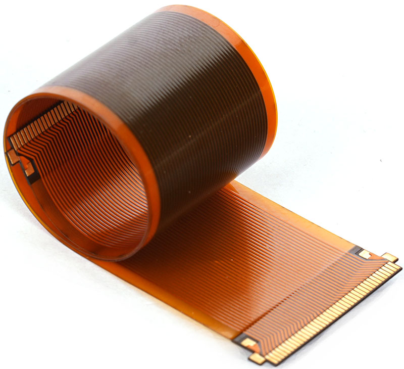
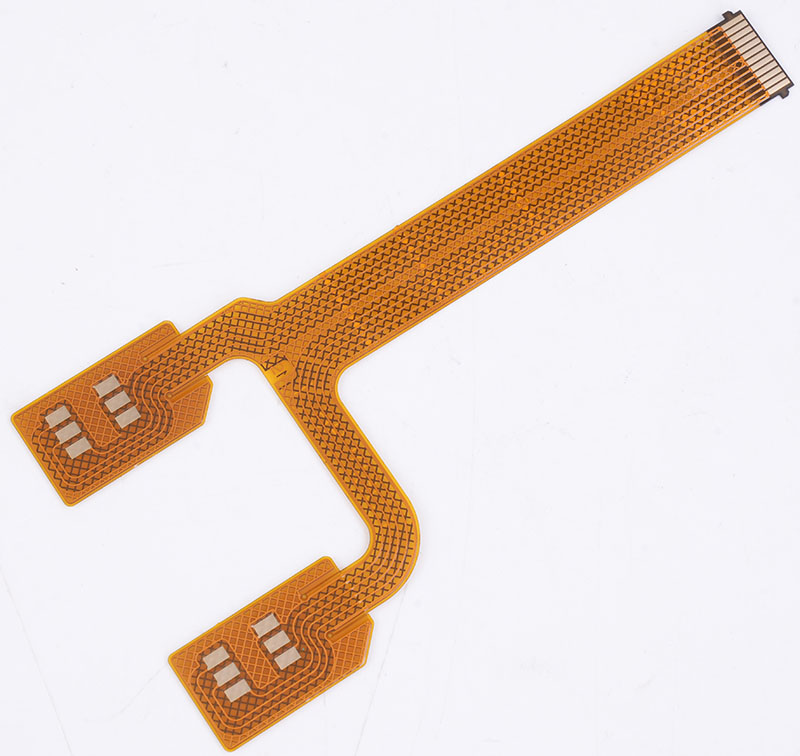
How Best Rigid-Flex PCB Assembly Services for Medical Devices Enhance Durability and Miniaturization?
Best rigid-flex pcb assembly services for medical devices unlock innovative form factors by combining rigid boards for component support with flexible circuits for dynamic movement and space savings.
- Enhancing Durability:
- Reduced Interconnections: Replacing fragile connectors and ribbon cables with soldered flex connections minimizes points of failure.
- Vibration/Shock Resistance: The flexible portions absorb and dissipate mechanical stress, protecting solder joints.
- Improved Reliability: A monolithic rigid-flex structure is more reliable than an assembly of multiple interconnected rigid boards.
- Enabling Miniaturization & Wearability:
- 3D Packaging: Boards can be folded into compact, three-dimensional shapes, crucial for implants, hearing aids, and endoscopic capsules.
- Weight Reduction: Eliminating connectors and using thin flex layers reduces overall weight—key for portable and wearable monitors.
- Dynamic Flexing: Allows for designs in hinged devices or probes that require repeated movement.
For a factory wholesale medical PCB assembly service, mastering rigid-flex is a key capability. It requires specialized PCB fab expertise for multilayer bonding and precise PCB assembly techniques to handle the delicate flex areas during soldering and handling.
Capabilities of a US Based PCB Assembly Partner for Healthcare OEMs
A US based PCB assembly partner provides a mature infrastructure, advanced engineering support, and tightly controlled manufacturing systems tailored for the demanding needs of Healthcare OEMs.
Advanced Engineering Collaboration
Localized teams provide rapid design reviews, DFM/DFA optimization, and direct engineering communication that shortens development cycles and reduces risk before prototypes are built.
Highly Controlled Manufacturing Processes
U.S. facilities apply strict process validation, IPC Class 3 manufacturing, real-time monitoring, and data-driven production oversight aligned with FDA and ISO 13485 expectations.
Robust Traceability and Documentation Systems
MES-based traceability, controlled documentation, and production records tailored for medical audits support DHF/DMR requirements and simplify compliance workflows.
Reliable Quick-Turn Prototyping and Small-Batch Production
Domestic fabrication and assembly resources enable consistent quick turn PCB USA results, accelerating verification testing and early clinical evaluations.
Secure and Verified Supply Chain
U.S. partners maintain qualified suppliers, validated sourcing protocols, and controlled inventory management to support long-term availability and stable BOM planning.
Specialized Medical Manufacturing Expertise
Experienced operators, medically trained technicians, and quality teams understand the expectations of Healthcare OEMs—from cleanliness requirements to test coverage and failure analysis.
A US based PCB assembly partner is not merely a vendor—it is a capability-driven extension of your R&D and manufacturing team, providing the technical depth, control, and confidence required for regulated medical devices.
How a Professional PCB Design Company Supports Medical Product Development from Concept to Verification?
A professional PCB design company is a vital co-pilot, transforming a conceptual medical device into a manufacturable, reliable, and certifiable product.
- Concept & Architecture: Advises on system partitioning, component selection, and technology (e.g., rigid-flex) to meet size, power, and cost targets.
- Schematic Capture & Simulation: Creates the electrical blueprint and runs signal/power integrity simulations to prevent performance issues.
- PCB Layout with DFM/DFA Rules: Engineers the physical board layout with strict adherence to medical-grade spacing, high-reliability routing, and, crucially, Design for Manufacturing/Assembly rules from the start.
- Design for Test (DFT): Incorporates test points and features to ensure the assembled board can be thoroughly validated.
- Documentation for Compliance: Generates the complete design history file (DHF) output needed for regulatory submission, including schematics, layouts, BOMs, and design rationale.
- Support through Verification & Validation (V&V): Works with the assembly partner to troubleshoot prototype builds and provide design revisions.
This end-to-end support de-risks development, ensuring the design is optimized not just for function, but for manufacturability and compliance from day one.
Why Many Healthcare Startups Seek Quick Turn PCB USA Solutions for Prototype Acceleration?
For healthcare startups, speed to proof-of-concept and clinical validation is critical for funding and market entry. Quick turn PCB USA services are the engine for this acceleration.
- Rapid Design Iteration: Fast prototype turns (e.g., 24-72 hours for fab, 5-10 days for assembly) allow engineers to test, discover flaws, and refine designs in quick succession.
- Faster Clinical & Regulatory Milestones: Functional prototypes are needed for benchtop testing, animal studies, and human trials. Faster builds compress the overall development timeline.
- Cost-Effective Exploration: Enables affordable testing of multiple design approaches or form factors before locking in final tooling for volume production.
- Attracting Investment: A working, refined prototype is far more compelling to investors than just a CAD model or idea.
By leveraging domestic quick turn PCB USA capabilities, startups maintain agility and momentum, turning innovative ideas into tangible devices with exceptional speed.
How Can a Factory Wholesale Medical PCB Assembly Service Ensure Consistent Quality and Compliance for Regulated Healthcare Devices?
A true factory wholesale medical PCB assembly service achieves consistent quality not through luck, but through a systemic, process-oriented approach built for the medical industry.
- Certified Quality Management System (QMS): Operation under ISO 13485:2016 is not optional; it’s the foundational framework that ensures consistent processes, corrective actions, and management oversight.
- Standardized Work Instructions & Process Validation: Every assembly step is defined, documented, and validated to prove it consistently produces a result meeting pre-defined specifications.
- Advanced Process Control & Monitoring: Solder paste inspection (SPI), automated optical inspection (AOI), and real-time thermal profiling of reflow ovens catch deviations in real-time.
- Rigorous Supplier Management: Components are sourced from approved vendors with full lot traceability. Incoming materials are inspected and certified.
- Independent Quality Assurance: A dedicated QA team, separate from production, performs audits and final releases based on data, not production schedules.
- Continuous Training: Personnel are regularly trained on medical device regulations, soldering standards (IPC-A-610 Class 3), and cleanroom protocols.
This holistic system transforms a factory wholesale operation from a cost center into a reliable, compliance-driven partner for regulated device manufacturing.
Why Partnering With a PCB Design Company Is Essential for Creating Safe and Reliable Medical Electronics?
Partnering with a PCB design company with medical expertise is essential because safety and reliability are designed in, not tested in. They bridge the gap between brilliant medical innovation and real-world, manufacturable hardware.
- Risk Mitigation by Design: Experts incorporate safety standards (like IEC 60601 for isolation and leakage currents) directly into the schematic and layout, designing out potential electrical hazards.
- Designing for Long-Term Reliability: They understand and design for factors like thermal management, signal integrity in noisy environments, and mechanical stress—all critical for devices that must work for years without fail.
- Avoiding Costly Late-Stage Re-Spins: Early DFM/DFA analysis prevents fundamental flaws that would require a complete board redesign after tooling is set, saving immense time and cost.
- Navigating Regulatory Documentation: Their deliverables become a core part of the technical file required for regulatory submission, ensuring the design is presented correctly to auditors.
Ultimately, this partnership ensures the electronic foundation of your medical device is as innovative, safe, and robust as the medical concept itself.
To sum up, medical PCB assembly services form the critical, reliable backbone of modern healthcare electronics, from life-sustaining implants to diagnostic equipment. This article has detailed how specialized expertise in design, fabrication, assembly, and testing converges to meet the unparalleled standards of the medical field.
Choosing a partner with deep medical market experience, robust quality systems, and a collaborative approach is not just a procurement decision—it’s a strategic investment in your product’s success and patient safety. As an ISO 13485:2016 certified specialist in medical PCB assembly services, EBest Circuit (Best Technology) combines engineering precision with regulatory insight to guide your device from prototype to volume production with unwavering quality. For more information or if you would like to send us any inquiry, please send us an email through the contact form at the bottom of our Contact Page.