Why choose PCB manufacturing Sweden? This guide explores benefits, types, certifications, top 2026 factories, and selection tips for reliable production.
Sweden is renowned for high-standard electronics manufacturing, and PCB manufacturing Sweden stands out for its precision and reliability. A professional PCB manufacturer in Sweden combines advanced technology with strict quality control to meet diverse project needs. Whether for industrial equipment or high-tech devices, PCB manufacturing Sweden delivers solutions that align with global standards. This guide covers key aspects of PCB Sweden services, helping you navigate the local market and select the right partner, including top Sweden PCB factory options and essential evaluation tips.
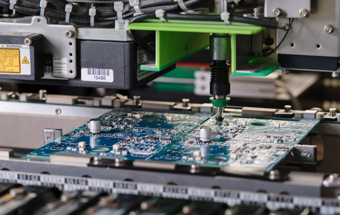
Why Choose PCB Manufacturing Sweden?
- Sustainable production practices with ISO 14001 certification, reducing environmental impact while ensuring compliance with EU regulations.
- Proximity to European electronics supply chains, cutting down component sourcing time by 30% compared to overseas manufacturers.
- Advanced quick-turn capabilities, supporting prototype and small-volume production with 2-7 working days lead time for common board types.
- Strict quality oversight with automated inspection processes, achieving a defect rate below 0.02% for mass production runs.
- Customized engineering support, including free DFM/DFA checks to optimize design for PCB Manufacturing Sweden processes.
- Compliance with automotive and medical industry standards, suitable for high-reliability application scenarios.
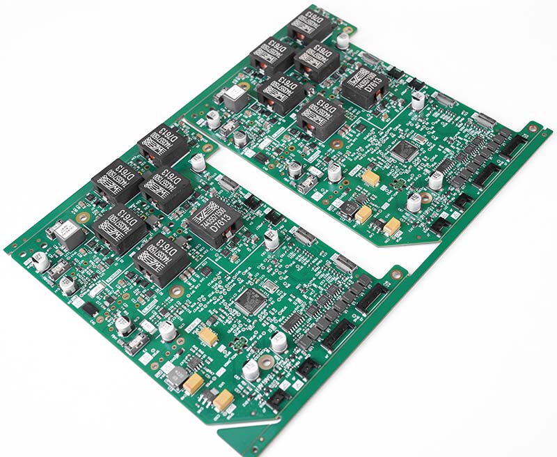
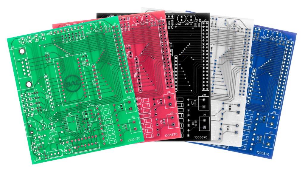
Types of PCB Manufacturing Sweden
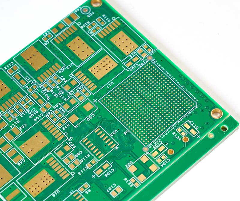
- Rigid PCBs: Single-layer, double-layer, and multilayer (up to 32 layers) for industrial control systems and automotive electronics.
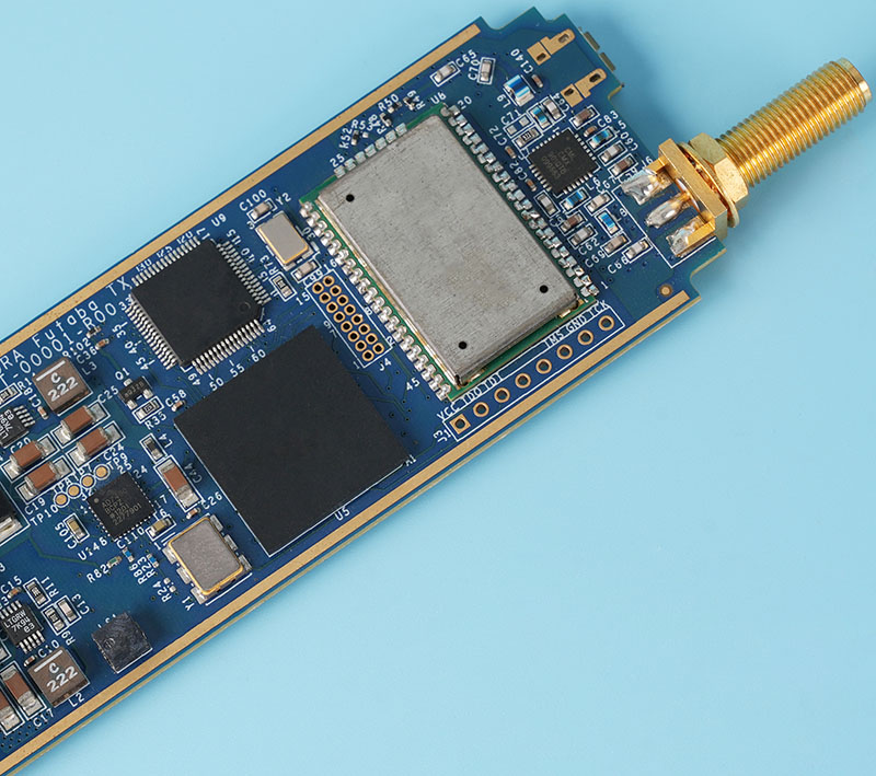
- Flexible & Rigid-Flex PCBs: Used in compact devices, with materials like Kapton for enhanced durability and bendability.
- HDI PCBs: High-density interconnect boards with microvias and impedance control, ideal for high-speed wireless devices.
- Metal Core PCBs: Aluminum-backed boards for LED lighting and power supplies, offering superior heat dissipation.
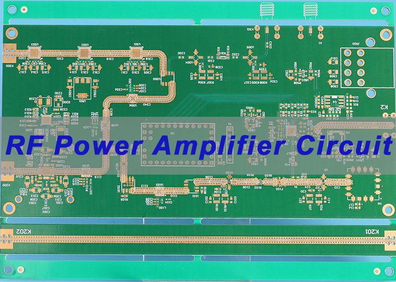
- RF & High-Frequency PCBs: Optimized for low signal loss, used in telecommunications and IoT equipment.
- Heavy Copper PCBs: Copper thickness up to 4oz, designed for high-power industrial applications.
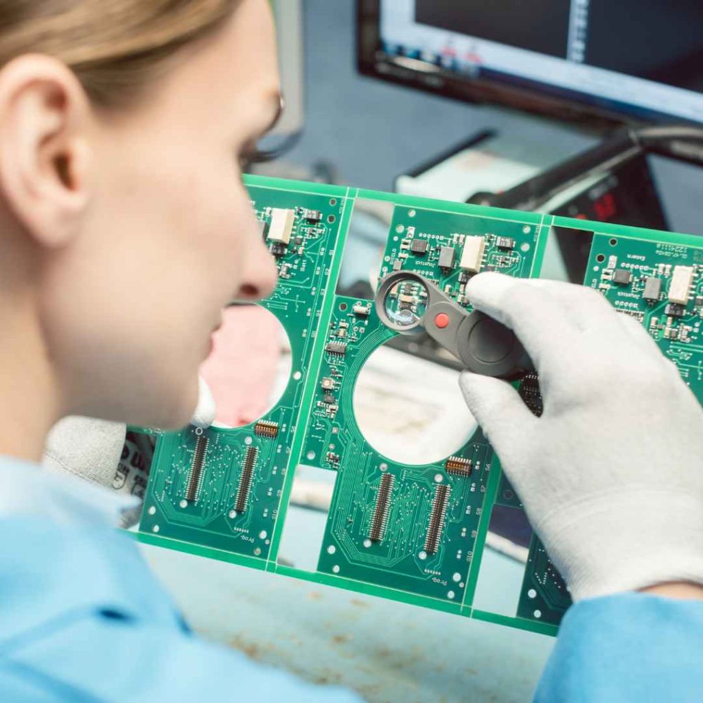
Quality Certifications in Swedish PCB Production
- ISO 9001:2015: Mandatory quality management system certification, ensuring consistent production processes, quality control and service standards across Sweden PCB manufacturing.
- UL Certification: A authoritative third-party electrical safety certification, equivalent to a “qualification certificate” for PCB materials, ensuring products meet global electrical safety requirements.
- ISO 14001: Environmental management system certification, reflecting the commitment of Sweden PCB Plant to sustainable production, reducing environmental impact and complying with EU environmental regulations.
- IPC Standards (IPC-A-600): Industry-specific standards governing PCB acceptability, covering design, production and inspection to ensure product consistency and reliability.
- ISO 45001: Occupational health and safety management system certification, safeguarding workplace safety during PCB production processes.
Top 10 PCB Factory in Sweden
| Company Name | Main Business | Core Advantage | Process Capability | Lead Time |
| EBest Circuit Co., Limited | Custom PCB fabrication, prototype and mass production | Global supply chain integration, cost-effectiveness | 1-32 layers, impedance control, buried/blind vias | Prototype: 2-5 days; Mass production: 7-15 days |
| ICAPE-MMAB | Prototype and small-volume PCB production | Sustainability-focused, long industry experience since 1970s | 1-14 layers, monthly capacity 550 sqm | 2L: 3-5 days; 4L: 4-6 days; 6L: 5-7 days |
| Elmatic AB | Custom PCB fabrication, SMT assembly for industrial electronics | Localized production support, ISO 9001/14001 certified | 1-16 layers, max panel 380x480mm, SMT assembly | Prototype: 4-6 days; Mass production: 8-12 days |
| NCAB Group Sweden AB | Multilayer, HDI and rigid-flex PCB production | Sustainable production, zero-defect commitment | 1-24 layers, RF and medical-grade PCBs | Prototype: 5-7 days; Mass production: 10-18 days |
| Note AB | Contract electronics manufacturing, PCB assembly | Medical and automotive industry expertise | 1-16 layers, SMT/THT assembly | 7-12 days for PCB + assembly |
| Intervalmercury | Precision PCB assembly and manufacturing | Fast turnaround, high build quality | 1-12 layers, mixed assembly services | Prototype: 3-5 days; Mass production: 8-14 days |
| SB Electro-Tech AB | Custom PCB production for industrial use | Local technical support, flexible customization | 1-8 layers, heavy copper up to 2oz | 5-10 days |
| Enics Sweden AB | Complete electronics manufacturing, PCB assembly | Full turn-key services, global footprint | 1-20 layers, high-volume production | 10-15 days for mass production |
| Prevas AB | Embedded systems, PCB design and manufacturing | IoT and automation solution integration | 1-16 layers, rigid-flex PCBs | 6-12 days |
| Mycronic AB | PCB assembly equipment and related PCBs | Advanced SMT equipment integration, high precision | 1-12 layers, high-mix production | 7-14 days |
How to Choose A Reliable PCB Factory in Sweden?
Below is A Guide to PCB Factory in Sweden:
1. Verify certifications comprehensively: Prioritize factories with ISO 9001:2015 (quality management) and ISO 14001 (environmental compliance). For automotive or medical projects, confirm IATF 16949 or ISO 13485 certifications. Check certificate validity via authorized bodies like RI.SE, such as NCAB Group Sweden AB which holds these certifications to ensure zero-defect consistency.
2. Inspect process capability details: Confirm layer range (1-16 layers for general needs, up to 32 layers for complex designs like EBest Circuit’s capability). Verify precision indicators: line width/spacing ≤ 3mil, minimum hole diameter 0.1mm, and impedance control ±10%. Ensure automated AOI/X-Ray inspection for micron-level process accuracy.
3. Evaluate lead time stability: Require a written on-time delivery rate ≥ 95% in the past 6 months. For urgent needs, check quick-turn options—ICAPE-MMAB offers 3-7 day delivery for 2-6 layer boards via local material stock and automated lines. Confirm contingency plans for supply chain disruptions.
4. Assess cost transparency: Request quotes itemized by material (FR-4/PTFE), testing, stencil, and logistics fees. Avoid hidden charges; EBest Circuit provides clear pricing with no stencil fees for prototypes. Confirm no additional costs for minor design adjustments.
5. Review after-sales service quality: Ensure free electrical testing (AOI, X-Ray, flying probe) and 24-hour technical support. Opt for factories offering pre-production DFM checks (like Elmatic AB’s free service) to reduce design errors. Confirm a minimum 1-year quality warranty for mass production batches.
How to Evaluate the Production Capacity of PCB Factory in Sweden?
Evaluation Guide to the Production Capacity of PCB Factory in Sweden:
- Monthly output capacity: Confirm sqm output (e.g., ICAPE-MMAB’s 550 sqm/month) to match your scale, this capacity fits small-batch industrial orders, while Enics Sweden AB suits high-volume demands.
- Layer processing capability: Align with design needs, 1-16 layers for general use (Elmatic AB’s scope), up to 32 layers for complex projects (EBest Circuit’s strength) like high-density industrial PCBs.
- Line width/spacing precision: Require ≤3mil for HDI PCBs, ensuring compatibility with high-speed signal transmission in IoT or telecom devices.
- Material adaptability: Verify support for PTFE (high-frequency RF PCBs)、FR-4 (industrial control) and optional aramid fiber (lightweight high-strength needs) to match product scenarios.
- Automation maturity: Prioritize factories with AOI/X-Ray inspection, achieving over 99% defect detection rate and keeping mass production defect rates below 0.02% (Sweden PCB manufacturing standard).
- Batch flexibility: Confirm prototype (1-100 pcs, ICAPE-MMAB’s quick-turn) and mass production (10,000+ pcs, Enics AB’s capacity) capabilities to cover full project cycles.
How to Evaluate the Delivery Time of PCB Manufacturer in Sweden?
Evaluation Guide to the Delivery Time of PCB Factory in Sweden:
- Quick-turn prototype lead time: 2-5 days for 2-4 layer PCB Sweden prototypes, consistent with ICAPE-MMAB’s 3-5 day turnaround for 2-layer boards.
- Normal mass production lead time: 7-15 days for 1-12 layer boards, matching Elmatic AB’s 8-12 day lead time for industrial PCBs.
- On-time delivery rate: Demand ≥95% on-time rate (past 6 months) with written verification from the Sweden PCB Factory.
- Emergency rush capability: Confirm 24-72 hour turnaround for critical prototypes, per Sweden’s quick-turn industry norms.
- Logistics reliability: Verify door-to-door delivery via reliable local logistics, with clear liability for PCB transit protection.
- Contractual clauses: Add penalty terms for delays exceeding 3 days, and clarify force majeure exceptions per industry standards.
Frequently Asked Questions About PCB Manufacturing Sweden
Q1: How to optimize PCB design to reduce PCB Manufacturing Sweden costs?
A1: Optimize panelization to maximize material utilization (e.g., 380x480mm panels used by Elmatic AB). Avoid non-standard sizes and minimize blind/buried vias. We offer free DFM checks to identify cost-saving opportunities. Contact us for a customized quote.
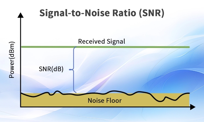
Q2: What causes signal interference in high-frequency PCB Sweden products, and how to solve it?
A2: Interference stems from improper layer stackup and impedance mismatch. We use high-frequency materials (PTFE) and control impedance within ±10%. Our engineering team optimizes trace routing to reduce crosstalk. Inquire for tailored high-frequency solutions.
Q3: Why do prototype lead times vary among Sweden PCB Factory options?
A3: Variations come from equipment automation and material stock. We maintain stock of common FR-4 materials and use automated lines for 2-4 layer prototypes, ensuring 2-3 day delivery. Request our prototype fast-track service via inquiry.
Q4: How to verify the quality of PCB Manufacturing Sweden products?
A4: We provide AOI, X-Ray, and electrical testing reports. For critical projects, third-party inspection by RI.SE is available. All products come with a quality guarantee. Contact us to learn about our testing processes.
Q5: Can Sweden PCB manufacturer support small-batch production with frequent design changes?
A5: Yes. We offer flexible small-batch production (10-500 pcs) with no minimum order quantity for repeat designs. Design change fees are waived for minor adjustments. Reach out for a flexible production quote.